EP0308869B1 - Verfahren zur Herstellung monokristalliner dünner Schichten aus LnA2Cu307-x mit einer Perovskit-Struktur mit 3 Ebenen - Google Patents
Verfahren zur Herstellung monokristalliner dünner Schichten aus LnA2Cu307-x mit einer Perovskit-Struktur mit 3 Ebenen Download PDFInfo
- Publication number
- EP0308869B1 EP0308869B1 EP88115399A EP88115399A EP0308869B1 EP 0308869 B1 EP0308869 B1 EP 0308869B1 EP 88115399 A EP88115399 A EP 88115399A EP 88115399 A EP88115399 A EP 88115399A EP 0308869 B1 EP0308869 B1 EP 0308869B1
- Authority
- EP
- European Patent Office
- Prior art keywords
- substrate
- single crystal
- thin film
- film
- plane
- Prior art date
- Legal status (The legal status is an assumption and is not a legal conclusion. Google has not performed a legal analysis and makes no representation as to the accuracy of the status listed.)
- Expired - Lifetime
Links
Images


Classifications
-
- C—CHEMISTRY; METALLURGY
- C30—CRYSTAL GROWTH
- C30B—SINGLE-CRYSTAL GROWTH; UNIDIRECTIONAL SOLIDIFICATION OF EUTECTIC MATERIAL OR UNIDIRECTIONAL DEMIXING OF EUTECTOID MATERIAL; REFINING BY ZONE-MELTING OF MATERIAL; PRODUCTION OF A HOMOGENEOUS POLYCRYSTALLINE MATERIAL WITH DEFINED STRUCTURE; SINGLE CRYSTALS OR HOMOGENEOUS POLYCRYSTALLINE MATERIAL WITH DEFINED STRUCTURE; AFTER-TREATMENT OF SINGLE CRYSTALS OR A HOMOGENEOUS POLYCRYSTALLINE MATERIAL WITH DEFINED STRUCTURE; APPARATUS THEREFOR
- C30B25/00—Single-crystal growth by chemical reaction of reactive gases, e.g. chemical vapour-deposition growth
- C30B25/02—Epitaxial-layer growth
-
- C—CHEMISTRY; METALLURGY
- C30—CRYSTAL GROWTH
- C30B—SINGLE-CRYSTAL GROWTH; UNIDIRECTIONAL SOLIDIFICATION OF EUTECTIC MATERIAL OR UNIDIRECTIONAL DEMIXING OF EUTECTOID MATERIAL; REFINING BY ZONE-MELTING OF MATERIAL; PRODUCTION OF A HOMOGENEOUS POLYCRYSTALLINE MATERIAL WITH DEFINED STRUCTURE; SINGLE CRYSTALS OR HOMOGENEOUS POLYCRYSTALLINE MATERIAL WITH DEFINED STRUCTURE; AFTER-TREATMENT OF SINGLE CRYSTALS OR A HOMOGENEOUS POLYCRYSTALLINE MATERIAL WITH DEFINED STRUCTURE; APPARATUS THEREFOR
- C30B29/00—Single crystals or homogeneous polycrystalline material with defined structure characterised by the material or by their shape
- C30B29/10—Inorganic compounds or compositions
- C30B29/16—Oxides
- C30B29/22—Complex oxides
- C30B29/225—Complex oxides based on rare earth copper oxides, e.g. high T-superconductors
-
- H—ELECTRICITY
- H10—SEMICONDUCTOR DEVICES; ELECTRIC SOLID-STATE DEVICES NOT OTHERWISE PROVIDED FOR
- H10N—ELECTRIC SOLID-STATE DEVICES NOT OTHERWISE PROVIDED FOR
- H10N60/00—Superconducting devices
- H10N60/01—Manufacture or treatment
- H10N60/0268—Manufacture or treatment of devices comprising copper oxide
- H10N60/0296—Processes for depositing or forming copper oxide superconductor layers
- H10N60/0576—Processes for depositing or forming copper oxide superconductor layers characterised by the substrate
- H10N60/0604—Monocrystalline substrates, e.g. epitaxial growth
Definitions
- the present invention relates to a process of producing a thin film of a single crystalline oxide of the formula: LnA2Cu3O 7-x (I) wherein Ln is at least one of the rare earth elements Y, Nd, Sm, Eu, Gd, Dy, Ho, Er, Tm and Yb and A is at least one of the alkaline earth metals Ba, Sr and Ca which has a three-layered perovskite structure.
- a thin film of LnA2Cu3O 7-x having a three-layered perovskite structure exhibiting superconductivity around 90 K will find various new applications such as wiring of LSI, SQUID and Josephson tunnel type elements.
- the LnA2Cu3O 7-x thin film should have a critical temperature Tc at 85 K or higher, a critical current density Jc of 105 A/cm2 or higher when the film is not thicker than 500 nm (5,000 ⁇ ) and should be formed at a comparatively low temperature.
- the single crystalline thin film should have a specific plane such as a (001), (110) or (103) plane parallel with a film plane so that electric current can flow in said specific plane.
- an insulating ultrathin layer between the superconductors for tunnel junction is required to have a thickness of not larger than 3 nm (30 ⁇ ).
- it is essential to produce a superconductive film having good surface smoothness and an ultrathin insulating layer on it.
- the thickness of the insulating ultrathin layer for forming a junction is limited by the coherence length of the superconductor.
- the coherence length in thedirection perpendicular to the (001) plane is about 0.4 to 0.7 nm (4 to 7 ⁇ ), and that in the direction parallel to said plane is about 1.5 to 3.0 nm (15 to 30 ⁇ ).
- the thickness of the insulating ultrathin layer to be used for junction varies with the kind of the superconductor and its crystal direction to be connected.
- the thickness of the latter should be 1.0 nm (10 ⁇ ) or less.
- the thickness of the latter can be as thick as several nm (ten ⁇ ), which makes the formation of tunnel junction easy. Accordingly, a (110) oriented single crystal film may be more available for the tunnel type junction than a (001) oriented film.
- the single crystalline film of LnA2Cu3O 7-x has been prepared by a sputtering method.
- the sputtering method comprises irradiating a plasma of oxygen (O2) and/or argon gas against a target consisting of a Ln-A-Cu base oxide in a vacuum vessel and depositing sputtered metals and the like on a substrate such as a SrTiO single crystal piece placed in said vessel to form a LnA2Cu3O 7-x thin film.
- a substrate such as a SrTiO single crystal piece placed in said vessel to form a LnA2Cu3O 7-x thin film.
- a superconductive oxide thin film is produced by electron beam deposition.
- the as-deposited film is amorphous and does not have superconductive characteristics as such. Therefore, the deposited film is post-heated at a high temperature of 800 to 1,000°C to crystallize the amorphous film to a perovskite crystal having a three-layered structure, whereby the produced film exhibits superconducting transition at 77 K or higher (see for example, Applied Physics Letters, Vol 51, No 11, 14 Sept. 1987, pp. 852-854).
- the target in the sputtering method, it is difficult to prepare the target with a composition optimum for the formation of the superconducting film. Since a desired material is deposited solely by attacking the target with ions, not only characteristics of the film are delicately changed according to conditions of the plasma atmosphere and to quality of the target, but also the substrate or the deposited film is easily modified by ions. Therefore, this method has poor reproducibility.
- the epitaxially grown LnA2Cu3O 7-x oxide film should be thermally treated at a temperature of 800°C or higher to increase the critical temperature to 77 K or higher, preferably 85 K or higher.
- the thermal treatment the surface of the thin film is roughened.
- the substrate material and LnA2Cu3O 7-x react with each other so that the thin layer having a thickness of 500 ⁇ or less cannot be made superconductive.
- a superconductive thin film which is produced by sputtering and subsequent thermal treatment at the lowest temperature is a 200 to 300 nm (2,000 to 3,000 ⁇ ) thick (001) oriented crystal film of YBa2Cu3O 7-x which is formed on a sapphire substrate heated at a temperature of 550 to 650°C. It is reported that this film had zero electric resistance at 80 K after thermally treated at a temperature of 550 to 650°C.
- the deposited film should be thermally treated at a high temperature. Therefore, the kind of the substrate to be used is limited. When the substrate is inadequate, it reacts with the deposited material so that a part or whole of the deposited material is changed to a material which is different from the superconductor.
- the surface of the deposited film is less smooth. Because of the reaction between the substrate and the deposited material, it is difficult to obtain the superconducting film with a thickness of 500 nm (5,000 ⁇ ) or less.
- the object of the present invention is to provide a process of producing a thin film of a LnA2Cu3O 7-x single crystal having the perovskite structure directly on a deposition substrate.
- a process of producing the above described thin film of the LnA2Cu3O 7-x single crystal which comprises generating plasma and simultaneously evaporating Ln, A and Cu in an atomic ratio of about 1:2:3 from discrete evaporation sources of Ln, A and Cu to deposit them on a single crystal substrate in a vacuum deposition vessel while supplying oxygen gas towards the substrate to form an oxygen-rich atmosphere having a pressure of 1.33 to 13.3 Pa (10 ⁇ 2 to 10 ⁇ 1 Torr) at the substrate.
- the single crystal used as the substrate has its (001) plane forming the substrate surface, and the (001) plane of the formed single crystal is parallel with the film surface; in another one in both cases (110) plane is used; in a third one the single crystal used as the substrate has its (110) plane forming the substrate surface, and the (103) plane of the formed single crystal is parallel with the film surface.
- oxygen content is not stoichiometric in the superconductive oxide of formula (I); oxygen may be present in a richer or poorer amount than the calculated stoichiometric amount.
- the microstructure namely a polycrystalline or a single crystalline structure in the formed thin film of LnA2Cu3O 7-x depends on the kind of the substrate.
- a single crystal of SrTiO3, MgO, CoO, NiO and the like having the (001) plane or the (110) plane in its surface is used as a substrate, respectively.
- the processes of producing the thin film of the LnA2Cu3O 7-x single crystal can be applied to the production of a polycrystalline LnA2Cu3O 7-x .
- the kind of the substrate is not limited.
- the substrate should have said specific crystal plane on its surface.
- the above requirements for the substrate are necessary conditions to make the specific crystal plane parallel with the substrate surface, but not sufficient conditions.
- Suitable conditions for producing the thin film of the LnA2Cu3O 7-x single crystal of the orientation (001) and those for producing the thin film of the LnA2Cu3O 7-x single crystal of the orientation (110) are different as follows:
- the raw material metals are evaporated and deposited on the substrate heated at 500°C or higher, while in the latter case, the raw material metals are evaporated and deposited on the substrate heated at a temperature not lower than 500°C and lower than 550°C to form the single crystalline LnA2Cu3O 7-x having the orientation (110) and, after raising the substrate temperature to 550°C or higher, the metals are further deposited on the already formed single crystal.
- the LnA2Cu3O 7-x single crystal having the orientation (001) can be produced under a relatively wide temperature range of 500°C or higher, preferably 520°C or higher but not so high as to adversely affect the substrate and the growing film. Thereby, a thin film having very good crystal structure is formed.
- the substrate is heated at a temperature not lower than 500°C and lower than 550°C, preferably around 530°C in the first evaporation step so as to render the new substrate of LnA2Cu3O 7-x thin film suitable for the formation of the desired material having the orientation (110) and, in the second step, the temperature at the new substrate is raised to 550°C or higher, preferably 600°C or higher. Under other conditions, no thin film having good superconductive characteristics is formed.
- the thin films formed in the first and second steps consist of the desired material
- the thin film produced in the first step is used as a base film in the second step and only the thin film formed in the second step has good superconductive characteristics.
- the first and second steps are not necessarily carried out continuously.
- the kind of the crystal plane is selected and the substrate temperatures are determined according to the orientation of the LnA2Cu3O 7-x single crystal to be formed on the substrate.
- the thin film of the LnA2Cu3O 7-x single crystal having the orientation (103) can be formed on the substrate at a higher temperature although the same crystal plane as in the case of the orientation (110) is used as the substrate. That is, to form the thin film of the LnA2Cu3O 7-x single crystal having the orientation (103), the thin film is deposited on the substrate heated at 550°C or higher, preferably 600°C or higher.
- the vacuum deposition vessel is firstly evacuated to high vacuum of, for example, about 1.33 x 10 ⁇ 4 Pa (10 ⁇ 6 Torr) and then a small amount of the oxygen gas is continuously supplied towards the substrate from a distance close to the substrate to increase the pressure of oxygen at the substrate to 1.33 to 13.3 Pa (10 ⁇ 2 to 10 ⁇ 1 Torr) while an interior gas in the vessel is continuously exhausted from a suitable part of the vessel to keep the background at 1.33 x 10 ⁇ 3 to 0.13 Pa (10 ⁇ 5 to 10 ⁇ 3 Torr) in the vessel except near the substrate.
- the reason why the upper limit of the background pressure is selected to be 0.13 Pa (10 ⁇ 3 Torr) is that Ln, A and Cu in the evaporation sources are constantly evaporated without deterioration of evaporation rates.
- the lower limit of 1.33 x 10 ⁇ 3 Pa (10 ⁇ 5 Torr). is the minimum gas pressure for generating the plasma. If the plasma is not utilized, this lower limit is not technically important.
- the reason why the oxygen gas pressure is increased only near the substrate in this embodiment is that Cu is not oxidized to Cu2+ if the oxygen gas pressure is lower than 0.13 Pa (10 ⁇ 3 Torr).
- the plasma can be generated by placing a high frequency coil between the evaporation sources and the substrate and oscillating it between the coil and the vessel wall at high frequency. While the plasma generation is preferred since reaction activities of the evaporated metals are increased, it may have some drawbacks such that the plasma attacks the desired material which is being formed if the plasma energy is too high. Therefore,the electric power for generating the plasma is preferably in a range from 50 to 500 W, preferably around 100 W.
- Ln and A are evaporated by the electron beam and Cu is evaporated by electric resistance heating.
- the atomic ratio of Ln, A and Cu is adjusted to about 1:2:3 by adjusting the electric power according to results of preliminary experiments. Namely, in the preliminary experiments, how much metal Ln, A or Cu is evaporated and how much oxide Ln2O3, AO or CuO is formed by the specific electric power applied to each evaporation source per unit time are measured by a film thickness measuring device installed in the vacuum evaporation vessel near the substrate for each metal. Thereby, a relationship between the evaporation rate of each metal and the applied electric power is established and then the electric power to be applied to each evaporation source during formation of the thin film of the LnA2Cu3O 7-x single crystal is determined.
- the process of the present invention can produce reproducibly the desired material since it can be carried out while preventing contamination with impurities under easily controlled operating conditions.
- the present invention has been completed based on the studies by the present inventors on the preparation and structures of thin films of oxide single crystals and their artificial superlattice thin films.
- the oxide thin film is formed by the reactive evaporation. This is because this method has been found to be most suitable for producing the desired material which is required to have a good crystalline quality.
- the reactive evaporation for preparing the oxide is a process comprising introducing the oxygen gas in the vacuum vessel, supplying metal atoms by evaporation on the substrate and forming the oxide while reacting the metal atoms with oxygen on the substrate.
- the reasons why the reactive evaporation is suitable for the formation of oxide thin film are that (a) the amount of oxygen in the oxide can be controlled and (b) a single crystal with good quality in crystallinity is formed.
- factors which determine the amount of oxygen in the oxide include the oxygen pressure, the substrate temperature, deposition rates of the metals and the kind of the substrate material. Since each of these factors can be changed independently from others, the amount of oxygen in the oxide can be freely adjusted.
- the reason (b) it has been found that when the single crystal is used as the substrate, a single crystal with excellent quality can be formed on the substrate. For example, when NiO is deposited on a sapphire C plane kept at 200°C under oxygen pressure of 5.32 x 10 ⁇ 2 Pa (4 x 10 ⁇ 4 Torr) at a deposition rate of 0.1 nm/sec (1 ⁇ /sec.), NiO single crystal is synthesized with the (111) plane being parallel with the substrate surface.
- a half value width in a rocking curve according to X-ray scattering on this single crystal is 0.5°.
- the half value width decreases to 0.06°. This means increase of crystallinity.
- the reactive evaporation has suitable characteristics for synthesizing a single crystal with good quality.
- the reason for this is assumed as follows:
- the condition (1) is achieved by (i) a small rate of crystal growth and (ii) preferential adsorption of the atoms onto high energy sites in the surface such as vacancies, kinks and steps.
- the condition (2) is easily satisfied by low temperature during crystal growth.
- condition (1) is achieved by following conditions:
- oxygen molecules are adsorbed only by metal atoms, they are always adsorbed by and desorbed from the crystal surface to establish equilibrium. On the contrary, generally once adsorbed metal atoms are not desorbed. However, the metal atoms having higher energy acquired in the evaporation source can sufficiently move over the crystal surface so that they are adsorbed by the high energy sites on the crystal surface. If the energy distribution of the metal atoms which arrive at the surface is narrow and the number of such metal atoms is decreased to such extent that each atom does not come into collision with other metal atoms on the surface, the condition (1) is achieved. To prevent the change of energy of the impinging metal atoms, the molecular beam is desirable if possible.
- the pressure is decreased to an order of 1.33 x 10 ⁇ 2 Pa (10 ⁇ 4 Torr) so as to increase their mean free path.
- a metal having a low evaporation temperature such as Zn
- the reactive evaporation has been found to be one of the best methods for controlling the crystal growth conditions of the oxide, and the present invention has been completed.
- a vacuum vessel having a diameter of 750 mm and a height of 1,000 mm was evacuated to 1.33 x 10 ⁇ 4 Pa (10 ⁇ 6 Torr) by an oil diffusion pump.
- a piece of sapphire (single crystal ⁇ -Al2O3) was used with the (0112) plane forming the substrate surface (10 mm x 10 mm). After placing the sapphire substrate in the vacuum vessel, it was heated to 650°C and kept at this temperature with a tungsten heater.
- the oxygen gas was directly blown onto the substrate, whereby the gas pressure was increased to 1.33 to 13.3 Pa (10 ⁇ 2 to 10 ⁇ 1 Torr) only near the substrate, while the pressure near the evaporation sources which were placed apart from the substrate was increased to about 1.33 x 10 ⁇ 2 Pa (10 ⁇ 4 Torr).
- Y, Ba and Cu were evaporated from independent evaporation sources at such evaporation rates that the atomic ratio of Y:Ba:Cu was 1:2:3 on the substrate.
- Y, Ba and Cu were evaporated at rates of 0.1 nm/sec (1 ⁇ /sec.), 0.23 nm/sec (2.3 ⁇ /sec.) and 0.17 nm/sec (1.7 ⁇ /sec.), respectively.
- a high-frequency (13.56 MHz) coil was placed, and high frequency was applied at 100 W so as to generate oxygen plasma, which activated the evaporated metals and accelerated the reactions on the substrate.
- the metal oxides were deposited on the substrate to form a thin film having a thickness of 100 nm (1,000 ⁇ ).
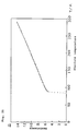
- FIG. 1 An X-ray diffraction pattern of the formed thin film is shown in Fig. 1.
- Peaks for (013), (103) and (110) which are specific to the YBa2Cu3O 7-x structure are clearly observed and the formation of a crystalline film is confirmed.
- Y and Ba were evaporated by an electron beam, and Cu was evaporated by resistance heating.
- the evaporation conditions were as follows: Y: A metal ingot (purity: 99.9 %) (50 g) was used and placed in a crucible cooled with water. The metal was evaporated by the application of an electron beam at an acceleration voltage of 5 KV and a filament current of 400 mA. Ba: A metal ingot (purity: 99.9 %) (50 g) was used and evaporated by the application of the electron beam at an acceleration voltage of 5 KV and a filament current of 100 mA.
- metal Cu particles particles size of 2 to 3 mm, purity of 99.9999 %) (10 g) were charged and heated by the application of electric current through the filament at 10 V, 30 A.
- a vacuum vessel having a diameter of 750 mm and a height of 1,000 mm was evacuated to 1.33 x 10 ⁇ 4 Pa (10 ⁇ 6 Torr). by an oil diffusion pump.
- the (001) plane of a SrTiO3 single crystal was used as a substrate (10 mm x 10 mm). After placing the substrate in the vacuum vessel, it was heated to 650°C and kept at this temperature with a tungsten heater.
- the oxygen gas was directly blown onto the substrate, whereby the gas pressure was increased to 1.33 to 13.3 Pa (10 ⁇ 2 to 10 ⁇ 1 Torr) only near the substrate, while the pressure near the evaporation sources which were placed apart from the substrate was increased to about 1.33 x 10 ⁇ 2 Pa (10 ⁇ 4 Torr).
- Y, Ba and Cu were evaporated from separate evaporation sources at such evaporation rates that the atomic ratio of Y:Ba:Cu was 1:2:3 on the substrate.
- Y, Ba and Cu were evaporated at rates of 0.1 nm/sec (1 ⁇ /sec.), 0.23 nm/sec (2.3 ⁇ /sec.) and 0.17 nm/sec (1.7 ⁇ /sec.), respectively.
- a high-frequency coil was placed, and high frequency was applied at 100 W so as to generate oxygen plasma, which activated the evaporated metals and accelerated the reactions on the substrate.
- the metal oxides were deposited on the substrate to form a 100 nm (1,000 ⁇ ) thick film.
- FIG. 2 An X-ray diffraction pattern of the formed thin film is shown in Fig. 2, in which "x2", “x1", “x4" and "x30" indicate how many times the intensities were magnified.
- the formed thin film was heated at 650°C for 30 minutes in the oxygen atmosphere and its critical current density at 77 K (liquid nitrogen temperature) was measured to find that it had the critical current density of 4 x 10⁶ A/cm2. This value was large in comparison with 1.8 x 10⁶ A/cm2 of the critical current density of the YBa2Cu3O 7-x type superconducting film made by sputtering.
- Example 2 In the same manner as in Example 2, a thin film of a YBa2Cu3O 7-x single crystal having the three-layered perovskite structure and a thickness of 300 nm (3,000 ⁇ ) was formed. After ten days from the formation of this thin film, the relationship between its resistivity and absolute temperature was measured. The results are shown in Fig. 3.
- the formed thin film exhibited superconductivity at a temperature slightly lower than 50 K. Such characteristics appear when an oxidation degree (X) is low. Further, it is apparent from Fig. 3 that the thin film had the orthorohmbic symmetry. After the thin film was heated to 500°C for 30 minutes in the oxygen atmosphere, its electric resistance became 0 (zero) at 90 K.
- the thin film of the single crystal of the present invention is different from the conventional ones and the produced thin film as such has superconductivity without post-heat-treatment at a high temperature of 900°C.
- two pieces of SrTiO3 single crystal were used, one of which had been surface polished and the other of which had been surface polished and further chemically etched with a mixture of hydrofluoric acid and nitric acid.
- the non-etched substrate, a thin film of 30 nm (300 ⁇ ) in thickness formed on it and a thin film of 100 nm (1,000 ⁇ ) in thickness formed on it were examined by a scanning electron microscope (SEM).
- SEM scanning electron microscope
- the etched substrate and the 100 nm (1,000 ⁇ ) thick film formed on it were examined by SEM, and it was found that the surface of the etched substrate had hillocks of several micrometers. Further, it was found that the SEM photograph of the thin film of 100 nm (1,000 ⁇ ) in thickness formed on the etched substrate was substantially the same as above and the thin film grew on the substrate with tracing the substrate surface exactly. This means that the deposition according to the present invention overgrew a uniformly thick film on the substrate surface and therefore made the smooth surface of the film on the same of substrate.
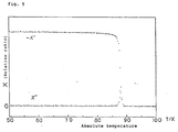
- Fig. 4 shows change of resistivity against temperature of a thin film having a thickness of 200 nm (2,000 ⁇ ) which was formed on the polished substrate and heat treated in the oxygen atmosphere in the same manner as in below described Example 5.
- a transition temperature as defined by zero resistivity was 90.2 K and the temperature range in which resistivity changed was as small as 1.7 K, which suggested that a superconductive thin film with excellent quality was formed.
- Fig. 5 shows change of complex susceptibility ⁇ ′ and ⁇ ⁇ against temperature of the same sample.
- a real part of the complex susceptibility (- ⁇ ′) sharply increased and simultaneously its imaginary part ( ⁇ ⁇ ) began to appear.
- the substrate on which the thin film of the LnA2Cu3O 7-x single crystal is formed preferably has a smoothly polished surface and, on such substrate, the superconductive thin film having a smooth surface and excellent quality can be formed, so that it will be particularly useful in the production of electrical devices such as a SQUID device and a Josephson device.
- the thin film just formed on the substrate does not necessarily exhibit good superconductivity, it is sometimes post-treated in an oxygen-containing atmosphere.
- Example 2 In the same manner as in Example 2 but using SrTiO3 with its (110) plane forming the surface and heating the substrate to 520°C, a thin film of YBa2Cu3O 7-x single crystal having a thickness of 200 nm (2,000 ⁇ ) was formed.
- the SEM photograph of the thin film of the single crystal was taken to confirm the surface smoothness.
- Example 2 In the same manner as in Example 1 but evaporating metals Y and Sr by electron beam heating and metal Cu by resistance heating and depositing them on the (001) plane of the SrTiO3 substrate kept at 640°C, a thin film having a thickness of 100 nm (1,000 ⁇ ) was formed.
- An X-ray diffraction pattern of the formed film is shown in Fig. 6, in which the diffraction peak corresponding to the (005) peak of the three layered perovskite structure like YBa2Cu3O 7-x .
- Example 2 In the same manner as in Example 2 but using Dy or Er in place of Y, a thin film was formed.
- the X-ray diffraction patterns were shown in Fig. 7 (for Dy) and Fig. 8 (for Er).
- the formed thin film in which Ln was Dy or Er was characterized in that the intensity of the (001) peak was stronger than that in the case where Ln was Y. This is because the spacing corresponding to the (001) peak is a spacing of the rare metal elements, so that, in case of Dy or Er having the larger atomic number, both the scattering factors for the X-ray are larger than that of Y and therefore the diffraction peak of (001) becomes stronger.
- Example 2 In the same manner as in Example 2 except that an injection nozzle was inserted in a doughnut shaped oxygen diffusion chamber surrounding the periphery of the substrate, and oxygen injected from the nozzle was once diffused in the chamber and then supplied from slits provided on an inner peripheral wall over the substrate surface, a thin film having a thickness of 10 nm (100 ⁇ ) was formed.
- the X-ray diffraction pattern of the formed thin film is shown in Fig. 9.
- the thin film was then post-heat-treated in the oxygen atmosphere in the same manner as in Example 5. Change of the electrical resistance against temperature of the oxidation-treated thin film is shown in Fig. 10, and change of the complex susceptibility against temperature of the same thin film is shown in Fig. 11.
- Example 9 In the same manner as in Example 9 but using, as a substrate, the SrTiO3 single crystal with a surface of its (110) plane and heating the substrate to 530°C, 550°C, 580°C or 630°C, a thin film having a thickness of 50 nm (500 ⁇ ) was formed.
- Figs. 12A, 13A, 14A and 15A (along the [001] direction) and Figs. 12B, 13B, 14B and 15B (along the [110] direction).
- Figs. 12A and 12B the thin film of YBa2Cu3O 7-x single crystal having the (110) plane which was parallel with the (110) plane of the substrate SrTiO3 single crystal was formed.
- Figs. 15A and 15B the thin film of YBa2Cu3O 7-x single crystal having the (103) plane which was parallel with the (110) plane of the substrate SrTiO3 single crystal was formed.
- the thin films containing a mixture of (110) and (103) orientations of the YBa2CU3O 7-x were formed.
- the thin film of YBa2Cu3O 7-x single crystal which was formed at 630°C and had a thickness of 50 nm (500 ⁇ ) was heat-treated in the oxygen atmosphere in the same manner as in Example 5 and change of the electrical resistance against temperature was measured. The results are shown in Fig. 16, which confirmed that the oxidation-treated thin film exhibited superconductivity around 80 K.
- Example 9 In the same manner as in Example 9 but using, as a substrate, the SrTiO3 single crystal with its (110) plane forming a surface and heating the substrate to 520°C, a thin film having a thickness of 15 nm (150 ⁇ ) was formed.
- Example 9 In the same manner as in Example 9 but using the substrate on which the thin film having a thickness of 15 nm (150 ⁇ ) as the substrate and heating the substrate to 630°C, a second thin film having a thickness of 85 nm (850 ⁇ ) was formed.
- Figs. 20A and 20B The results are shown in Figs. 20A and 20B. As seen from these figures, a thin film of YBa2Cu3O 7-x single crystal having the (110) plane which was parallel with the (110) plane of the substrate SrTiO3 single crystal was formed.
- the thin film of YBa2Cu3O 7-x single crystal having the thickness of 85 nm (850 ⁇ ) was heat-treated in an oxygen atmosphere in the same manner as in Example 5 and change of the electrical resistance against temperature was measured. The results are shown in Fig. 21, which confirmed that the oxidation-treated thin film exhibited superconductivity around 80 K.
Landscapes
- Chemical & Material Sciences (AREA)
- Crystallography & Structural Chemistry (AREA)
- Engineering & Computer Science (AREA)
- Organic Chemistry (AREA)
- Materials Engineering (AREA)
- Metallurgy (AREA)
- Inorganic Chemistry (AREA)
- Manufacturing & Machinery (AREA)
- Chemical Kinetics & Catalysis (AREA)
- General Chemical & Material Sciences (AREA)
- Crystals, And After-Treatments Of Crystals (AREA)
- Superconductor Devices And Manufacturing Methods Thereof (AREA)
- Superconductors And Manufacturing Methods Therefor (AREA)
Claims (8)
- Verfahren zur Herstellung einer dünnen Schicht, bestehend aus einem monokristallinen Oxid-Supraleiter der Formel (I)
LnA₂Cu₃O7-x
wobei Ln mindestens eines der Seltenerdelemente Y, Nd, Sm, Eu, Gd, Dy, Ho, Er, Tm und Yb bedeutet und A mindestens eines der Erdalkalimetalle Ba, Sr und Ca bedeutet, mit einer dreischichtigen Perowskit-Struktur, umfassend das gleichzeitige Verdampfen von Ln, A und Cu in einem Atomverhältnis von etwa 1:2:3 aus einzelnen Verdampferquellen für Ln, A und Cu, um sie in einem Vakuumgefäß auf einem Einkristallsubstrat abzuscheiden, wobei Sauerstoffgas gegen das Substrat geleitet wird, um am Substrat eine sauerstoffreiche Atmosphäre mit einem Druck von 1,33 bis 13,3 Pa zu erzeugen. - Verfahren nach Anspruch 1, umfassend ferner die Erzeugung eines Plasmas während des Schrittes des gleichzeitigen Verdampfens von Ln, A und Cu in einem Atomverhältnis von etwa 1:2:3 aus einzelnen Verdampferquellen für Ln, A und Cu.
- Verfahren nach einem der Ansprüche 1 und 2, wobei die (001) Ebene des als Substrat verwendeten Einkristalls die Substratoberfläche bildet und die (001) Ebene des erzeugten Einkristalls zur Schichtoberfläche parallel ist.
- Verfahren nach Anspruch 3, wobei das Substrat während der Abscheidung der Schicht auf eine Temperatur von nicht unter 500°C erhitzt wird.
- Verfahren nach einem der Ansprüche 1 und 2, wobei die (110) Ebene des als Substrat verwendeten Einkristalls die Substratoberfläche bildet und die (110) Ebene des erzeugten Einkristalls zur Schichtoberfläche parallel ist.
- Verfahren nach Anspruch 5, wobei zuerst eine dünne Schicht des Einkristalls des Oxids der Formel (I), dessen (110) Ebene parallel zur Schichtoberfläche ist, auf dem, während der Abscheidung der Schicht auf eine Temperatur von nicht unter 500°C und unter 550°C erhitzten, Substrat erzeugt wird und danach ein Oxid der Formel (I), dessen (110) Ebene parallel zur Schichtoberfläche ist, auf der zuerst erzeugten, auf eine Temperatur nicht unter 550°C erhitzten, dünnen Schicht abgeschieden wird.
- Verfahren nach einem der Ansprüche 1 und 2, wobei die (110) Ebene des als Substrat verwendeten Einkristalls die Substratoberfläche bildet und die (103) Ebene des erzeugten Einkristalls zur Schichtoberfläche parallel ist.
- Verfahren nach Anspruch 7, wobei das Substrat während der Abscheidung der Schicht auf eine Temperatur von nicht unter 550°C erhitzt wird.
Applications Claiming Priority (14)
| Application Number | Priority Date | Filing Date | Title |
|---|---|---|---|
| JP23679387 | 1987-09-21 | ||
| JP236793/87 | 1987-09-21 | ||
| JP23679287 | 1987-09-21 | ||
| JP236792/87 | 1987-09-21 | ||
| JP314670/87 | 1987-12-11 | ||
| JP31467087 | 1987-12-11 | ||
| JP31807487 | 1987-12-15 | ||
| JP318074/87 | 1987-12-15 | ||
| JP33630/88 | 1988-02-15 | ||
| JP3363088 | 1988-02-15 | ||
| JP57207/88 | 1988-03-10 | ||
| JP5720788 | 1988-03-10 | ||
| JP63075486A JP2704625B2 (ja) | 1987-09-21 | 1988-03-28 | 三層ペロブスカイト構造をもつLnA▲下2▼Cu▲下3▼O▲下7▼−xの単結晶薄膜及びLnA▲下2▼Cu▲下3▼O▲下7▼−x薄膜の製造法 |
| JP75486/88 | 1988-03-28 |
Publications (3)
| Publication Number | Publication Date |
|---|---|
| EP0308869A2 EP0308869A2 (de) | 1989-03-29 |
| EP0308869A3 EP0308869A3 (en) | 1990-10-31 |
| EP0308869B1 true EP0308869B1 (de) | 1995-05-31 |
Family
ID=27564353
Family Applications (1)
| Application Number | Title | Priority Date | Filing Date |
|---|---|---|---|
| EP88115399A Expired - Lifetime EP0308869B1 (de) | 1987-09-21 | 1988-09-20 | Verfahren zur Herstellung monokristalliner dünner Schichten aus LnA2Cu307-x mit einer Perovskit-Struktur mit 3 Ebenen |
Country Status (3)
| Country | Link |
|---|---|
| EP (1) | EP0308869B1 (de) |
| CA (1) | CA1322514C (de) |
| DE (1) | DE3853905T2 (de) |
Families Citing this family (12)
| Publication number | Priority date | Publication date | Assignee | Title |
|---|---|---|---|---|
| JP2896193B2 (ja) * | 1989-07-27 | 1999-05-31 | 株式会社東芝 | 酸化物結晶配向膜の製造方法及び酸化物結晶配向膜並びに光磁気記録媒体 |
| EP0410627A1 (de) * | 1989-07-27 | 1991-01-30 | Kabushiki Kaisha Toshiba | Oxidfilm mit bevorzugter Kristallausrichtung, Verfahren zu dessen Herstellung und magnetooptisches Aufzeichnungsmaterial |
| JPH11186623A (ja) * | 1997-12-25 | 1999-07-09 | Sumitomo Electric Ind Ltd | 磁気センサ |
| US6436317B1 (en) | 1999-05-28 | 2002-08-20 | American Superconductor Corporation | Oxide bronze compositions and textured articles manufactured in accordance therewith |
| US6562761B1 (en) | 2000-02-09 | 2003-05-13 | American Superconductor Corporation | Coated conductor thick film precursor |
| AU1325001A (en) | 1999-07-23 | 2001-02-13 | American Superconductor Corporation | Methods of making a superconductor |
| US6765151B2 (en) | 1999-07-23 | 2004-07-20 | American Superconductor Corporation | Enhanced high temperature coated superconductors |
| US6828507B1 (en) | 1999-07-23 | 2004-12-07 | American Superconductor Corporation | Enhanced high temperature coated superconductors joined at a cap layer |
| US6730410B1 (en) | 1999-08-24 | 2004-05-04 | Electronic Power Research Institute, Incorporated | Surface control alloy substrates and methods of manufacture therefor |
| US6974501B1 (en) | 1999-11-18 | 2005-12-13 | American Superconductor Corporation | Multi-layer articles and methods of making same |
| US6673387B1 (en) | 2000-07-14 | 2004-01-06 | American Superconductor Corporation | Control of oxide layer reaction rates |
| US20020056401A1 (en) | 2000-10-23 | 2002-05-16 | Rupich Martin W. | Precursor solutions and methods of using same |
-
1988
- 1988-09-20 CA CA000577966A patent/CA1322514C/en not_active Expired - Fee Related
- 1988-09-20 EP EP88115399A patent/EP0308869B1/de not_active Expired - Lifetime
- 1988-09-20 DE DE3853905T patent/DE3853905T2/de not_active Expired - Fee Related
Non-Patent Citations (5)
| Title |
|---|
| APPLIED PHYSICS LETTERS, vol. 51, no. 11, 14 September 1987, New York, US, pp. 852-854; B. OH et al.: "Critical current densities and transport in superconducting YBa2Cu307-d films made by electron beam coevaporation" * |
| APPLIED PHYSICS LETTERS, vol. 51, no. 26, 28 December 1987, New York, US, pp. 2263-2265; H. ADACHI et al.: "Low-temperature process for the preparation of high Tc superconducting thin films" * |
| JAPANESE JOURNAL OF APPLIED PHYSICS, vol. 26, no. 5, May 1987, Tokyo, JP, pp. 876-878; M. ONODA et al.: "Crystal structures of YBa2Cu30x and LnBa2Cu30x(Ln=Ho and Dy)" * |
| JAPANESE JOURNAL OF APPLIED PHYSICS, vol. 26, no. 7, July 1987, Tokyo, pp. 1248-1250; Y. ENOMOTO et al.: "Largely anisotropic superconducting critical current in epitaxially grown Ba2YCu3O7-y thin film" * |
| JAPANESE JOURNAL OF APPLIED PHYSICS, vol. 27, no. 1, January 1988, Tokyo, pp. 91-93; T. TERASHIMA et al.: "Single-crystal YBa2Cu3O7-x thin films by activated reactive evaporation" * |
Also Published As
| Publication number | Publication date |
|---|---|
| EP0308869A3 (en) | 1990-10-31 |
| DE3853905D1 (de) | 1995-07-06 |
| DE3853905T2 (de) | 1995-10-12 |
| CA1322514C (en) | 1993-09-28 |
| EP0308869A2 (de) | 1989-03-29 |
Similar Documents
| Publication | Publication Date | Title |
|---|---|---|
| EP1735847B1 (de) | Biaxial texturierte filmabscheidung für supraleiterbeschichtete bänder | |
| US6663976B2 (en) | Laminate articles on biaxially textured metal substrates | |
| JP2009035479A (ja) | 金属オキシフッ化物の超伝導性酸化物への制御された変換 | |
| WO1991003323A1 (en) | Plasma deposition of superconducting thick films | |
| EP0308869B1 (de) | Verfahren zur Herstellung monokristalliner dünner Schichten aus LnA2Cu307-x mit einer Perovskit-Struktur mit 3 Ebenen | |
| JP2986799B2 (ja) | 薄膜形成方法及び薄膜形成装置 | |
| US6794339B2 (en) | Synthesis of YBa2CU3O7 using sub-atmospheric processing | |
| JPH02255525A (ja) | Y系超伝導薄膜の製造方法 | |
| US5453306A (en) | Process for depositing oxide film on metallic substrate by heat plasma flash evaporation method | |
| US5061687A (en) | Laminated film and method for producing the same | |
| US5362711A (en) | Method for producing single crystal superconducting LnA2 Cu3 O7-x films | |
| JP2704625B2 (ja) | 三層ペロブスカイト構造をもつLnA▲下2▼Cu▲下3▼O▲下7▼−xの単結晶薄膜及びLnA▲下2▼Cu▲下3▼O▲下7▼−x薄膜の製造法 | |
| EP0416545B1 (de) | Verbundfilm und dessen Herstellungsverfahren | |
| JP2639544B2 (ja) | 三層ペロブスカイト構造をもつLaA▲下2▼Cu▲下3▼O▲下7▼▲下−▼xの単結晶薄膜及びLaA▲下2▼Cu▲下3▼O▲下7▼▲下−▼x薄膜の製造法 | |
| US5716908A (en) | Process for controlling crystalline orientation of oxide superconductive film | |
| KR970009739B1 (ko) | 고온초전도박막의 제조방법 | |
| EP0329103B2 (de) | Verfahren zur Herstellung von dünnen Schichten aus Hochtemperatur-Supraleiteroxyd | |
| JP2715667B2 (ja) | 酸化物超電導薄膜製造装置および酸化物超電導単結晶薄膜の製造方法 | |
| JP2919956B2 (ja) | 超電導部材の製造方法 | |
| EP0407941A1 (de) | Einkristalline Dünnschicht von Ln2-xCexCuO4-y und Verfahren zu ihrer Herstellung | |
| JPH02255534A (ja) | Bi系超伝導薄膜の製造方法 | |
| EP1111691A2 (de) | Supraleiter und zugehöriges Vorläufermaterial, deren Herstellung und Verwendung des Supraleiters | |
| JPH01208323A (ja) | 薄膜製造法 | |
| JPH02255527A (ja) | Ti系超伝導薄膜の製造方法 | |
| Chern | Synthesis of yttrium barium copper oxide superconducting thin films by metalorganic chemical vapor deposition |
Legal Events
| Date | Code | Title | Description |
|---|---|---|---|
| PUAI | Public reference made under article 153(3) epc to a published international application that has entered the european phase |
Free format text: ORIGINAL CODE: 0009012 |
|
| AK | Designated contracting states |
Kind code of ref document: A2 Designated state(s): BE CH DE FR GB IT LI NL |
|
| PUAL | Search report despatched |
Free format text: ORIGINAL CODE: 0009013 |
|
| AK | Designated contracting states |
Kind code of ref document: A3 Designated state(s): BE CH DE FR GB IT LI NL |
|
| 17P | Request for examination filed |
Effective date: 19910417 |
|
| 17Q | First examination report despatched |
Effective date: 19930910 |
|
| RAP1 | Party data changed (applicant data changed or rights of an application transferred) |
Owner name: TOYO BOSEKI KABUSHIKI KAISHA Owner name: TOSOH CORPORATION Owner name: TDK CORPORATION Owner name: NIPPON STEEL CORPORATION Owner name: JAPAN ENERGY CORPORATION Owner name: NEC CORPORATION Owner name: MATSUSHITA ELECTRIC INDUSTRIAL CO., LTD. Owner name: KANEGAFUCHI CHEMICAL INDUSTRY CO., LTD. |
|
| GRAA | (expected) grant |
Free format text: ORIGINAL CODE: 0009210 |
|
| RAP1 | Party data changed (applicant data changed or rights of an application transferred) |
Owner name: TOYO BOSEKI KABUSHIKI KAISHA Owner name: TOSOH CORPORATION Owner name: TDK CORPORATION Owner name: NIPPON STEEL CORPORATION Owner name: JAPAN ENERGY CORPORATION Owner name: NEC CORPORATION Owner name: MATSUSHITA ELECTRIC INDUSTRIAL CO., LTD. Owner name: KANEGAFUCHI CHEMICAL INDUSTRY CO., LTD. |
|
| AK | Designated contracting states |
Kind code of ref document: B1 Designated state(s): BE CH DE FR GB IT LI NL |
|
| ITF | It: translation for a ep patent filed | ||
| REF | Corresponds to: |
Ref document number: 3853905 Country of ref document: DE Date of ref document: 19950706 |
|
| ET | Fr: translation filed | ||
| PLBE | No opposition filed within time limit |
Free format text: ORIGINAL CODE: 0009261 |
|
| STAA | Information on the status of an ep patent application or granted ep patent |
Free format text: STATUS: NO OPPOSITION FILED WITHIN TIME LIMIT |
|
| 26N | No opposition filed | ||
| PGFP | Annual fee paid to national office [announced via postgrant information from national office to epo] |
Ref country code: BE Payment date: 19970812 Year of fee payment: 10 |
|
| PGFP | Annual fee paid to national office [announced via postgrant information from national office to epo] |
Ref country code: CH Payment date: 19970902 Year of fee payment: 10 |
|
| PG25 | Lapsed in a contracting state [announced via postgrant information from national office to epo] |
Ref country code: LI Free format text: LAPSE BECAUSE OF NON-PAYMENT OF DUE FEES Effective date: 19980930 Ref country code: CH Free format text: LAPSE BECAUSE OF NON-PAYMENT OF DUE FEES Effective date: 19980930 Ref country code: BE Free format text: LAPSE BECAUSE OF NON-PAYMENT OF DUE FEES Effective date: 19980930 |
|
| BERE | Be: lapsed |
Owner name: SEISAN KAIHATSU KAGAKU KENKYUSHO Effective date: 19980930 Owner name: KANEGAFUCHI CHEMICAL INDUSTRY CO. LTD Effective date: 19980930 |
|
| REG | Reference to a national code |
Ref country code: CH Ref legal event code: PL |
|
| REG | Reference to a national code |
Ref country code: GB Ref legal event code: IF02 |
|
| PGFP | Annual fee paid to national office [announced via postgrant information from national office to epo] |
Ref country code: FR Payment date: 20030730 Year of fee payment: 16 |
|
| PGFP | Annual fee paid to national office [announced via postgrant information from national office to epo] |
Ref country code: GB Payment date: 20030910 Year of fee payment: 16 |
|
| PGFP | Annual fee paid to national office [announced via postgrant information from national office to epo] |
Ref country code: NL Payment date: 20030930 Year of fee payment: 16 Ref country code: DE Payment date: 20030930 Year of fee payment: 16 |
|
| PG25 | Lapsed in a contracting state [announced via postgrant information from national office to epo] |
Ref country code: GB Free format text: LAPSE BECAUSE OF NON-PAYMENT OF DUE FEES Effective date: 20040920 |
|
| PG25 | Lapsed in a contracting state [announced via postgrant information from national office to epo] |
Ref country code: NL Free format text: LAPSE BECAUSE OF NON-PAYMENT OF DUE FEES Effective date: 20050401 Ref country code: DE Free format text: LAPSE BECAUSE OF NON-PAYMENT OF DUE FEES Effective date: 20050401 |
|
| GBPC | Gb: european patent ceased through non-payment of renewal fee |
Effective date: 20040920 |
|
| PG25 | Lapsed in a contracting state [announced via postgrant information from national office to epo] |
Ref country code: FR Free format text: LAPSE BECAUSE OF NON-PAYMENT OF DUE FEES Effective date: 20050531 |
|
| NLV4 | Nl: lapsed or anulled due to non-payment of the annual fee |
Effective date: 20050401 |
|
| REG | Reference to a national code |
Ref country code: FR Ref legal event code: ST |
|
| PG25 | Lapsed in a contracting state [announced via postgrant information from national office to epo] |
Ref country code: IT Free format text: LAPSE BECAUSE OF NON-PAYMENT OF DUE FEES;WARNING: LAPSES OF ITALIAN PATENTS WITH EFFECTIVE DATE BEFORE 2007 MAY HAVE OCCURRED AT ANY TIME BEFORE 2007. THE CORRECT EFFECTIVE DATE MAY BE DIFFERENT FROM THE ONE RECORDED. Effective date: 20050920 |