EP0310088B1 - Système à boucle d'asservissement de phase numérique - Google Patents
Système à boucle d'asservissement de phase numérique Download PDFInfo
- Publication number
- EP0310088B1 EP0310088B1 EP88116121A EP88116121A EP0310088B1 EP 0310088 B1 EP0310088 B1 EP 0310088B1 EP 88116121 A EP88116121 A EP 88116121A EP 88116121 A EP88116121 A EP 88116121A EP 0310088 B1 EP0310088 B1 EP 0310088B1
- Authority
- EP
- European Patent Office
- Prior art keywords
- signal
- output
- frequency
- phase
- frequency dividing
- Prior art date
- Legal status (The legal status is an assumption and is not a legal conclusion. Google has not performed a legal analysis and makes no representation as to the accuracy of the status listed.)
- Expired - Lifetime
Links
- 230000004044 response Effects 0.000 claims description 8
- 238000001514 detection method Methods 0.000 claims description 7
- 238000010586 diagram Methods 0.000 description 14
- 230000002349 favourable effect Effects 0.000 description 3
- 230000006870 function Effects 0.000 description 2
- 230000007257 malfunction Effects 0.000 description 2
- 238000013139 quantization Methods 0.000 description 2
- 230000002411 adverse Effects 0.000 description 1
- 230000003252 repetitive effect Effects 0.000 description 1
- 239000011435 rock Substances 0.000 description 1
- 230000001360 synchronised effect Effects 0.000 description 1
Images


Classifications
-
- H—ELECTRICITY
- H03—ELECTRONIC CIRCUITRY
- H03L—AUTOMATIC CONTROL, STARTING, SYNCHRONISATION OR STABILISATION OF GENERATORS OF ELECTRONIC OSCILLATIONS OR PULSES
- H03L7/00—Automatic control of frequency or phase; Synchronisation
- H03L7/06—Automatic control of frequency or phase; Synchronisation using a reference signal applied to a frequency- or phase-locked loop
- H03L7/08—Details of the phase-locked loop
- H03L7/099—Details of the phase-locked loop concerning mainly the controlled oscillator of the loop
- H03L7/0991—Details of the phase-locked loop concerning mainly the controlled oscillator of the loop the oscillator being a digital oscillator, e.g. composed of a fixed oscillator followed by a variable frequency divider
- H03L7/0992—Details of the phase-locked loop concerning mainly the controlled oscillator of the loop the oscillator being a digital oscillator, e.g. composed of a fixed oscillator followed by a variable frequency divider comprising a counter or a frequency divider
Definitions
- This invention relates to a digital phase-locked loop system in which a phase-locked loop (PLL) is composed of digital circuit elements.
- PLL phase-locked loop
- phase-locked loop systems Many types have been released recently. These digital phase-locked loop systems have a phase-locked loop composed of digital circuit elements. In comparison with analog type systems, such digital type systems have advantages that scatter due to parts used is insignificant and that desired characteristics can be obtained without necessity of adjustment.
- digital phase-locked loop systems an output from a stationary oscillator is frequency-divided and outputted as an output from the loop, and therefore the phase-locked loop can be operated only by input frequencies in the range below one several-tenth of a maximum frequency for operating a logical circuit element incorporated therein.
- a digital phase-locked loop system having the features defined in the preamble of appended claims 1 and 4 is known from the US patent US-A-4,538,119.
- Fig. 18 shows an example of a similar phase-locked loop system, having also the features of the preamble of appended claim 1, for operating at a fraction (1/N, N: a positive integer) of a frequency of a traditional stationary oscillator (OSC) 4.
- OSC stationary oscillator
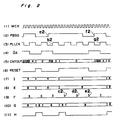
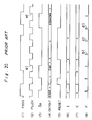
- Clock pulse MCK which is an output of the stationary oscillator 4 is shown in Fig. 19 (1), input signal PBSG in Fig. 19 (2), and phase-locked loop clock signal PLLCK in Fig. 19 (3).
- Signal Q ⁇ A from an output terminal Q ⁇ of the D-type flip-flop 3 is shown in Fig. 22 (4).
- Clock pulse MCK, input signal PBSG, and output signal Q ⁇ A of a D-type flip-flop 3 are applied to an AND gate G1 and an output of the AND gate G1 is supplied to a clock input terminal CK of the counter 1.
- Output signal CNTOUT of the counter 1 is shown in Fig. 19 (5).
- Output signal U of a frequency divider 7 is applied to a clock input terminal CK of a D-type flip-flop 8 and is also applied to the clock input terminal CK of the D-type flip-flop 3 through an inversion circuit N1 and then drawn out as phase-locked loop clock signal PLLCK.
- Output of an AND gate G2 is applied to the counter 1 and register 5 as reset signal RESET.
- the reset signal RESET is as shown in Fig. 19 (6).
- Fig. 19 there exists a phase difference in the time interval between a step-up edge "a" of the input signal PBSG and a step-up edge "b" of the phase-locked loop clock signal PLLCK and this time interval is counted by the counter 1.
- the input signal PBSG, output signal Q ⁇ A from the D-type flip-flop 3 which latches the input signal PBSG at the step-up or leading edge of the phase-locked loop clock signal PLLCK, and clock pulses MCK from the stationary oscillator 4 are applied to the AND gate G1 before the clock input into the counter 1, by which the counter 1 provided with the output of the AND gate 1 counts the time between the edges a -b.
- the counter 1 counts the pulses from the AND gate G1 until reset signal RESET from the other AND gate G2 is inputted.
- Output from a terminal Q of the D type flip-flop 8 which latches the output from a terminal Q of the D type flip-flop 3 at the step-up edge of the signal U and the output from the terminal Q of the D type flip-flop 3 are applied to the AND gate G2 and the signal CNTOUT which represents the counted value of the counter 1 is latched by the register 5 at the step-up edge of the reset signal RESET from the AND gate G2.
- Phase difference signal I outputted from the register 5 is shown in Fig. 19 (7), which is applied to a decoder 6 and decoded.
- Load signal E outputted by the decoder 6 is as shown in Fig. 19 (8), which signal is loaded in the frequency divider 7 as a frequency dividing rate for the frequency divider 7.
- the clock pulse MCK from the stationary oscillating circuit 4 is frequency-divided by a value represented by the phase difference signal I indicative of the difference between the input signal APBSG and phase-locked loop clock signal PLLCK, and then a frequency dividing rate of the frequency divider 7 generating the phase-locked loop clock signal APLLCK is changed to another one, so that phases of the input signal PBSG and phase-locked loop clock signal PLLCK are kept so as to agree with each other.
- the frequency dividing rate of the frequency divider 7 is N when the phases of the input signal PBSG and phase-locked loop clock signal PLLCK agree, and the rate becomes N + 1 or N - 1 depending on the degree of the phase difference so that the phases agree with each other.
- the frequency divider 7 gets loaded with the load signal E representing the frequency dividing rate applied from the decoder 6 in response to load clock signal F.
- This load clock signal F is generated as shown in Fig. 19 (9) by the logical circuit 9 when the output signal U of the frequency divider 7 represents a specified value.
- load signal E representing frequency division ratio 9 is applied to the frequency divider 7 from the decoder 6 at the time point c, and the phase difference is corrected to zero at the time point d.
- Fig. 20 (3) shows the output signal Q ⁇ A of the D type flip-flop 3
- Fig. 20 (4) shows the output signal CNTOUT of the counter 1
- Fig. 20 (5) shows the reset signal RESET
- Fig. 20 (6) shows the phase difference signal I outputted by the register 5
- Fig. 20 (7) shows the load signal E representing a frequency dividing rate of the decoder 6
- Fig. 20 (8) shows the load clock signal F from the logical circuit 9.
- the phase difference at the point of time al is corrected at the points of time b1, c1, and d1 in the same way and therefore the phase becomes reversed in polarity at the point of time b1 which gives adverse influence on the phase-locked loop characteristics.
- the frequency divider is supplied by said switching means at first with a first frequency dividing rate corresponding to a detected phase difference, and is then supplied with a second frequency dividing rate which is either a constant value or a value outputted by a frequency dividing rate adjusting means.
- the frequency divider is supplied by the switching means with one of two frequency dividing rates in dependence of one of two speed modes of the input signal.
- the digital phase-locked loop system functions as follows: it sets a frequency dividing rate by the output from the frequency dividing rate setting means when a phase difference occurs, corrects this frequency dividing rate once or more by a predetermined number of times, and thereafter gives a predetermined frequency division constant from a frequency division constant setting means, such as the frequency division rate at normal time, to the frequency divider so that the frequency divider rate is not corrected. This enables the system to minimize the deviation of phases between the input signal and the phase-locked loop clock signal.
- a frequency dividing rate corresponding to the phase difference between the input signal and the phase-locked loop clock signal is set by the frequency dividing rate setting means and the frequency divider is operated according to it.
- a frequency dividing rate setting means can count the time interval between a leading edge of the input signal and a leading edge of the phase-locked loop clock signal and set the frequency dividing rate.
- the frequency dividing rate adjusting means detects changes in the minimum repetitive frequency of the input signal PBSG by shifting with the clock signal from the oscillator, for instance, and determines the frequency dividing rate based on the frequency components of this input signal.
- the frequency dividing rate switching means first operates the frequency divider in accordance with the frequency dividing rate which is set by the frequency dividing rate setting means when a phase difference is detected, and then operates the same at the frequency dividing rate which is set by the frequency dividing rate adjusting means.
- a simple composition can cope with wide changes in frequencies of input signals with favorable characteristics without significant deviation in phase between the input signals and phase-locked loop clock signals, and it can prevent unlocking of the phase-locked loop.
- Phase changes may also arise when it is necessary to cope with at least two types of input signals reproduced in different speed modes.
- the arrangement is, according to claim 4, such that when a phase difference detection signal is provided, the phase difference detection signal is decoded by one of at least two decoders and loaded as a frequency dividing rate value of the frequency divider which generates the phase-locked loop clock.
- the decoder actually being used is switched according to the speed mode of the input signal to the other one having different decoding characteristics.
- a decoder is selected that makes much correction of the frequency dividing rate when the phase deviation amount is large, but little correction when the phase deviation amount is small in normal mode for usual reproduction, and a decoder to correct the frequency dividing rate approximately in proportion to the phase deviation amount is selected in a search mode due to large fluctuation of speed.
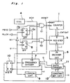
- Fig. 1 is a block diagram of this embodiment.
- clock pulse MCK from the stationary oscillator 4 is generated as shown in Fig. 2 (1) and input to the AND gate G1.
- Input signal PBSG has a waveform as shown in Fig. 2 (2), is applied to the input terminal D of the D type flip-flop 3 as well as to the AND gate G1.
- the D type flip-flop 3 draws the logical value which was applied to the input terminal D when phase-locked loop clock signal PLLCK was input to the clock input terminal CK to the output terminal Q and signal Q ⁇ A is output from the inverting output terminal Q ⁇ .
- This output signal Q ⁇ A of the D type flip-flop 3 is applied to the AND gate G1.
- the output of the AND gate G1 is input to the counter 1.
- the output signal Q ⁇ A of the D type flip-flop 3 is as shown in Fig. 2 (4).
- the counter 1 counts the pulses applied through the AND gate G1 and the counted value is applied to the register 5 as output signal CNTOUT as shown in Fig. 2 (5).
- Output signal U of the frequency divider 7 is drawn out as phase-locked loop clock signal PLLCK through the inverting circuit N1 and input to the clock input terminal CK of another D type flip-flop 8 at the same time.
- Signal of the output terminal Q of the D type flip-flop 3 is input to the input terminal D of the D type flip-flop 8 and applied to the AND gate G2 also.
- Signal from the output terminal Q of the D type flip-flop 8 is also applied to the AND gate G2.
- Output of the AND gate G2 is input as reset signal RESET of the counter 1 and applied to the register 5 at the same time.
- the register 5 stores output signal CNTOUT of the counter 1 when the output of the AND gate G2 is input and draws out phase difference signal I to the decoder 6.
- Reset signal RESET which is output from the AND gate G2 is as shown in Fig. 2 (6) and phase difference signal I of the register 5 is shown in Fig. 2 (7).
- the phase difference signal I of the register 5 is input to the decoder 6.
- Output E of the decoder 6 is as shown in Fig. 2 (8).
- the output U of the frequency divider 7 is applied to the logical circuit 9.
- the logical circuit 9 draws out the load clock signal F which has waveform as shown in Fig. 2 (9).
- the frequency divider 7 receives the load signal G representing frequency dividing rate when the load clock signal F is input, frequency-divides the clock pulse MCK from the stationary oscillator 4 and draws out the signal U.
- the decoder 6 decodes a value obtained by counting the clock pulses MCK from the stationary oscillator 4 for the time from the step-up edge of the input signal PBSG to the step-up edge of the phase-locked loop clock signal PLLCK and applies decoded data to the frequency divider 7 through the data switching circuit 11.
- the load signal G representing frequency dividing rate applied to the frequency divider 7 from the data changer 11 is shown in Fig. 2 (10). Frequency dividing rate is also shown in Fig. 2 (10).
- RS flip-flop 10 is set by the output of the AND gate G2 and reset by the load clock signal F from the logical circuit 9.
- Signal H from the output terminal Q of this RS flip-flop 10 is as shown in Fig. 2 (11) and applied to the data switching circuit or data changer 11.
- the data switching circuit 11 applies the output E from the decoder 6 to the frequency divider 7 as load signal G representing frequency dividing rate when the signal H is high level and applies signal representing frequency dividing rate of a predetermined constant N from the constant setting circuit 12 to the frequency divider 7 as load signal G when the signal H is low level.
- Constant N is "8" in this embodiment for instance.
- clock pulse MCK from the stationary oscillating circuit 4 is input to the counter 1 through the AND gate G1 and counted and its output signal CNTOUT is applied to the register 5.
- step-up waveform of the reset signal RESET is obtained from the AND gate G2, and by the waveform output "3" of the counter 1 is stored in the register 5, phase difference signal D of the register 5 is applied to the decoder 6, and output E representing frequency dividing rate "9" is drawn out from the decoder 6.
- the RS flip-flop 10 draws out high level signal H in response to the reset signal RESET from the AND gate G2. Therefore, the data switching circuit 11 is applied with the output E from the decoder 6 as load signal G of the frequency divider 7 and loaded in the frequency divider 7 at the point of time c2 shown in Fig. 2 (9) according to the load clock signal F from the logical circuit 9.
- the frequency divider 7 conduct frequency dividing operation at the frequency dividing rate "9" in this way.
- the R-S flip-flop 10 is reset at the point of time c2 at the step-down edge of the load clock signal F from the logical circuit 9. Therefore, the data switching circuit 11 applies the signal presenting constant N from the constant setting circuit 12 to the frequency divider 7 as load signal G. At the time points d2 and e2 when load clock signal F of the logical circuit 9 is drawn out, constant N is loaded to the frequency divider 7 and frequency dividing operation at N is conducted.
- the system is composed so that output E from the decoder 6 is loaded to the frequency divider 7 only once when phase difference occurs caused between input signal PBSG and phase-locked loop clock signal PLLCK.
- it may be composed so that RS flip-flop 10 is reset after plural number of load clock signal F of the logical circuit 9 are generated, output E of the decoder 6 is loaded to the frequency divider 7 predetermined multiple number of times, and then load signal G from the data switching circuit 11 is loaded to the frequency divider 7.
- frequency dividing rate corresponding to the phase difference between input signal and phase-locked loop clock signal is set and loaded to the frequency divider from frequency dividing rate changing circuit and thereafter a predetermined frequency dividing rate value from the frequency dividing rate constant setting means is set to the frequency divider, and therefore increase of phase difference is prevented, phase of the phase-locked loop clock signal coincides with that of input signal and characteristics of the phase-locked loop system is improved.
- Composition of this embodiment is relatively simple and therefore can be operated sufficiently near the limit of response speed of logical circuit components.
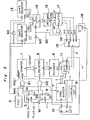
- Fig. 3 is a general block diagram of this embodiment. This embodiment is partially similar to the composition shown in Fig. 1. Therefore parts of this embodiment corresponding to the composition of the embodiment are indicated with a reference mark and the explanation is omitted. Notable in this embodiment is that two shift registers 20 and 13 are provided to detect frequency components of the input signal PBSG based on the clock pulse MCK of the stationary oscillator 4. The input signal PBSG is input to the data input terminal D of these shift registers 20 and 13 respectively.
- the input signal PBSG is applied to the clock input terminal CK for the shift register 20 on one side and to the clock input terminal CK through the inverting circuit N2 to other shift register 13.
- These shift registers 20 and 13 count the number of clock pulses input to the clock input terminal CK during the term while high-level signal is being applied to the data input terminal D and shift the input signal PBSG in succession.
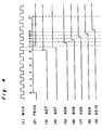
- the waveform of the clock pulse MCK from the stationary oscillator 4 is shown in Fig. 4 (1) and the waveform of the input signal PBSG in Fig. 4 (2).
- the output of the 7th cell of the shift register 20 to be AQ7, output of the 8th cell to be AQ8, the output of the 9th cell to be AQ9, and the output of the 10th cell to be AQ10 they are shown in Fig. 4 (3, (5), (7), and (9) respectively.
- Output of the shift registers 12 and 13 are collectively shown by the reference marks AQ and BQ respectively. These outputs are applied to the latch circuit 14.
- Clock pulse MCK from the stationary oscillator 4 is inverted by the inverting circuit N3 and input to the clock input terminal CK of the latch circuit 14 and the output AQ and BQ of the shift registers 12 and 13 are respectively latched based on this clock input signal.
- the numeral assigned to the input signal PBSG in Fig. 4 (2) indicates the number of clock signals from the stationary oscillator 4, that is the length of the high-level term.
- the signals latched by the latch circuit 14 vary, as shown in Table 1 below according to the number of clock pulses 7 - 9 and 2T of the stationary oscillator 4 in the length of term where the input signal PBSG is at high level by 0.5 step. This result corresponds to frequencies of the input signal PBSG.
- T is the number of pulses of the clock signal, "8" from the stationary oscillator 4, which is the expected cycle value of the input signal PBSG.
- Fig. 5 (1) - (9) show the signal waves corresponding respectively to Fig. 4 (1) - (9).
- Fig. 5 shows a a case that the phase of the input signal PBSG (refer to Fig. 5 (2)) is deviated from the input signal PBSG in Fig. 4 (refer to Fig. 4 (2)).
- the input signal PBSG is digitally modulated and include those of twice or 3 times the expected cycle T.
- the above described embodiment shows a case of 2T in maximum cycle.
- the decoder 15 applies 3 bits in total, output B1, B2, and B3, in response to the output of the latch circuit 14 and applies the output K suitable to the cycle of 2T or more to OR gate 16.
- the output of the inverting circuit N3 is also applied to this OR gate 16 through the line 30.
- the output of the OR gate 16 is input to the clock input terminal CK of the latch circuit 17.
- the latch circuit 17 latches the output B1, B2, and B3 of the decoder 15 only when the output K is logical "0", that is, only when the term of high level of the input signal PBSG is between the number of pulses 7 - 9 of the stationary oscillator 4. This enables to prevent malfunction when the term of high level of the input signal PBSG is more than 2T.
- the Output A11, A12, and A13 from the latch circuit 17 correspond respectively to the output A1, A2, and A3 of the decoder 15 and are input to the read only memory (ROM) 19.
- Another signal A10 is output from the output terminal Q of the T type flip-flop (TFF) 18 and input to the read only memory 19.
- the load clock signal F from the logical circuit 9 is applied to the T type flip-flop 18 also and the T type flip-flop 18 inverts the logical state of the signal of the output terminal Q every time of receiving the load clock signal F.
- This read only memory 19 receives the previously described signals A10 - A13 as address signal, draws out the output R of 4 bits from the output terminal Q, and applies it to the data switching circuit 11. Contents of the read only memory 19 are shown in Table 2.
- the output R of the read only memory 19 varies according to the input. Such state is shown in Figs. 6 - 8.
- Fig. 6 (1) shows the waveform of the clock pulse MCK of the stationary oscillator 4
- Fig. 6 (2) shows the waveform of the input signal PBSG
- Fig. 6 (3) shows the waveform of the phase-locked loop clock signal PLLCK.
- the output signal Q ⁇ A of the D type flip-flop 3 is shown in Fig. 6 (4) and the output CNTOUT of the counter 1 is shown in Fig. 6 (5).
- the reset signal RESET from the AND gate G2 is shown in Fig. 6 (6).
- the phase difference signal D of the register 5 is shown in Fig. 6 (7) and the output E of the decoder 6 is shown in Fig. 6 (8).
- the load clock signal F of the logical circuit 9 is shown in Fig. 6 (9).
- the signal H from the output terminal Q of the RS flip-flop 10 is shown in Fig. 6 (11). When this signal H is at high level, the output E of the decoder 6 is loaded to the frequency divider 7 as load signal G, and when the output H is at low level, the data switching circuit 11 loads the output R of the read only memory 19 to the frequency divider 7 as load signal G.
- the load signal G is shown in Fig. 6 (10).
- Fig. 7 (1) - (11) and Fig. 8 (1) - (11) correspond to each waveform of above described Fig. 6 (1) - (11).
- the output R of the read only memory 19 outputs alternately "8" and "9" as load signal G.
- phase-locked loop rock range is remarkably improved to the variation of the frequencies of the input signal PBSG within the range and unlocking is prevented.
- the output of the read only memory 19 is drawn out alternately as “8” and “9", and “7” and “8", in order to make the frequency of the input signal PBSG 7.5 or 8.5 times the clock pulse MCK of the stationary oscillator 4.
- the output of the read only memory 19 is drawn out in other mode as another embodiment of this invention, locking corresponding to the cycle of the input signal PBSG becomes possible corresponding to the cycle of the input signal PBS.
- frequency dividing rate corresponding to the phase difference between input signal and phase-locked loop clock signal is set by the frequency dividing rate changing circuit, and then frequency dividing rate corresponding to frequency components of the input signal is determined and the frequency divider is operated under the frequency dividing rate adjusting means. Therefore, even though an input signal varies and drifts in a wide range, phase-locked loop can be locked at favorable characteristics, phase deviation between input signal and phase-locked loop clock signal can be prevented, with simple composition.
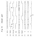
- FIG. 9 A third embodiment of this invention is shown referring to Figs. 9 to 15.
- Fig. 9 is a block diagram showing electrical composition of the digital PLL system 101 of this embodiment similar to the composition of the first and second embodiments as shown in Figs. 1 and 3 respectively.
- Figs. 10 and 11 are timing charts showing waveforms of signals at each part. Operation of this embodiment is described below referring to Figs. 9, 10, and 11.
- One of the features of this embodiment is that a plural number of shift registers 116 and 117 are provided to detect the frequency components of the input signal PBSG based on the clock pulse MCK of the stationary oscillator 102.
- the input signal PBSG is input to the data input terminal d of the said shift registers 116 and 117 respectively through line L1.
- the waveform shown in Fig. 10 (1) shows the waveform of the clock signal MCK output from the stationary oscillator 102.
- the input signal PBSG input to the first shift register 116 is shifted in succession by the clock signal MCK as shown in Fig. 10 (2).
- the input signal PBSG input to the second shift register 117 is shifted in succession at the timing of the negative phase clock signal M ⁇ C ⁇ K ⁇ when the said clock signal MCK is inverted by the inverter 115 as shown in Fig. 11 (1).
- the shift output AQ and BQ output in succession after being shifted in this way are input to the data input terminal da and db of the latch circuit 118 separately and latched at the timing at the step-down edge of the said input signal PBSG.
- output AQ7 - AQ10 of the first shift register 116 are shown in Fig. 10 (3), (5), (7) and (9), and, assuming the output corresponding to 7th to 9th of the second shift register 117 respectively to be BQ7 - BQ9, the output BQ7 - BQ9 of the second shift register 117 are shown in Fig. 10 (4), (6) and (8).
- Figure 0, 1, 2, 3, .... attached to the waveform of the input signal PBSG in Fig. 10 (2) show the number counted by the said clock signal MCK during the term when the input signal PBSG is at high level, that is the length of high level term of the input signal PBSG.
- Signals latched to the latch circuit 118 vary in 0.5 steps to the counted Nos. 7 - 9 and 2T by the said clock signal MCK while the input signal PBSG is at high level, as shown in table 3, according to the length during the high level term of the input signal PBSG and the result corresponds to the frequency of the input signal PBSG.
- Fig. 11 (1) - (9) show the waveforms corresponding to those in Fig. 10 (1) - (9) in which the phase of the input signal PBSG is deviated from that shown in Fig. 10.
- the input signal PBSG is digital modulated and those twice and three times those 1 cycle T are also included. This embodiment shows a case of 2T.
- the decoder 119 applies 3 bits of output A1, A2, and A3 respectively and separately to the shift register 122, 123, and 124 in response to the output of the latch circuit 118 and applies the signal K corresponding to the cycle 2T or more to the OR gate 121, and the OR gate 121 prepares shift clock signal SCK by the logical summation of the said signal K and clock signal MCK inverted by the inverter 120.
- A1, A2 and A3 output to the shift register 122, 123, and 124 are shifted only when the signal K output from the said decoder 119 is 0, that is, only when the term at high level of the input signal PBSG is 7 - 9 as shown in Table 3, whereby preventing malfunction in the section more than 2T in cycle.
- the decode output A1, A2, and A3 of the said decoder 119 shifted by the shift register 122 are input to vote takers 125, 126, and 127 respectively.
- the vote takers 125 - 127 are realized by a plural number of NAND gates shown in Fig. 12, for instance, and outputs values occupying 2 of 3 inputs as shown in the truth table in Table 4, by which decoded values of the said decoder 119 can be detected more accurately.
- the load data signal R to determine the frequency dividing rate of the frequency divider 103 is prepared by decoding the output A10 of the T flip-flop circuit 129 which conducts toggle operation by the output A11, A12, and A13 from the vote takers 125, 126, and 127 and load clock signal F output from the logical circuit 113, by the read only memory (referred to as ROM hereafter).
- addresses of the ROM128 are designated by the output A11, A12 and A13 of the vote takers 125, 126, and 127, and the output A of the T flip-flop circuit 129 and the output Q of the ROM 128 is input to the data changer 112 as load data signal R.
- Contents of the ROM128 are as shown in Table 5.
- the load data signal R which is its output, varies.
- the condition of the variation is shown in Figs. 13, 14, and 15.
- Table 5 A13 A12 A11 A10 Output R of ROM128 Cycle of PBSG 0 0 0 0 9 7 0 0 0 1 0 0 1 0 8 7.5 0 0 1 1 9 0 1 0 0 8 8 0 1 0 1 0 1 1 0 7 8.5 0 1 1 1 8 1 0 0 0 7 9 1 0 0 1 1
- Fig. 13 (1) shows the waveform of the clock signal MCK which is the output of the stationary oscillator 102
- Fig. 13 (2) shows the waveform of the input signal PBSG
- Fig. 13 (3) shows the waveform of the PLL clock signal PLLCK.
- the output Q ⁇ A of the first D-FF circuit 105 is shown in Fig. 13 (4) and the output CNTOUT of the counter 107 is shown in Fig. 13 (5).
- the reset signal RST output from the AND gate 110 is shown in Fig. 13 (6), and the waveform of the output signal I of the register 108 is shown in Fig. 13 (7).
- the waveform of the output signal E of the decoder 111 is shown in Fig. 13 (8), output signal F of the logical circuit 113 in Fig. 13 (9), and the control signal H output from the flip-flop circuit 114 is shown in Fig. 13 (11).
- the data changer 112 inputs the data of the output signal E of the decoder 111 to the frequency divider 103 as load signal G and when the control signal H is at low level, inputs the output signal R of the ROM 128 to the frequency divider 103 as load signal G.
- the waveform of the load signal G is as shown in Fig. 13 (10).
- Fig. 14 (1)-(11) and Fig. 15 (1)-(11) correspond to above described each waveform in Fig. 13 (1)-(11).
- the output R of the ROM 128 outputs "8" and "9” alternately and apply them to the frequency divider 103 through the data changer 112 as load signal G.
- the output R of the ROM 128 is "9" as shown in Fig. 14, which is input to the frequency divider 103 as the load signal G.
- two shift registers 116 and 117 are used and the frequency detecting accuracy of the input signal PBSG can be increased to a half of the clock signal MCK of the stationary oscillator 102 by them.
- the detecting accuracy of the input signal PBSG can be further improved.
- the output of the ROM 128 is drawn out alternately as “8", “9", and “7”, “8", in order to make the frequency of the input signal PBSG 7.5 or 8.5 times the clock signal MCK of the stationary oscillator 102.
- the output of the ROM 128 in other mode as another embodiment of this invention, locking can be effected under individual control corresponding to the cycle of the input signal PBSG.
- phase locked loop (PLL) system since a frequency dividing rate corresponding to phase difference between input signal and PLL clock signal is set by the frequency dividing rate setting circuit and then the frequency dividing rate corresponding to the frequency components of the input signal is set by the frequency dividing rate adjusting means, such a phase locked loop (PLL) system can be realized that locking of the PLL can be done with favorable characteristics even if the input signal varies in wide range and drifts, even for input signals of high speed near the limit of the processing speed of the logical circuit and even though the circuit composition is simple.
- PLL phase locked loop
- Fig. 16 is a circuit diagram showing a digital PLL system according to this embodiment
- Fig. 17 is a timing chart showing operation of this circuit.
- the digital PLL system of this embodiment is used to read signals reproduced in the normal mode and search mode in DAT, etc.
- reproduced signal PBSG is input to the D-flip-flop 201, latched there at the step-up edge of the reproducing clock PLLCK input to the clock terminal (CK) and input to the AND gate 202 together with the inversion output ( Q ⁇ A) of the D flip-flop 201.
- Basic clock MCK output from the stationary oscillator 203 has been input to this AND gate 202 and logical product of the 3 input signals, PBSG, Q ⁇ A, and MCK, is obtained. This logical product is made the clock input to the counter 204.
- the counter 204 counts the phase difference between the reproducing signal PBSG and reproducing PLL clock PLLCK (term from the step-up edge 5 of PBSG to the step-up edge 6 of PLLCK in Fig. 17) with the basic clock MCK as the unit.
- Logical product of the Q output of the D flip-flop 207 which latches the Q output of the said D flip-flop 201 at the step-up edge of the signal of PLLCK inverted again ( PLLCK ⁇ ) and the Q output of the said D flip-flop 201 is obtained by the AND gate 208.
- This logical product (called RESET signal) becomes clock of the register 209 which latches the output CNTOUT of the said counter 204.
- This clock becomes the RESET signal to the counter 204 at the same time, the counter 204 is reset by this RESET signal, and the next counting operation is started from the step-up edge 5 of the next PBSG.
- the said CNTOUT is latched synchronously with the step-up edge of the RESET signal.
- the said PLLCK ⁇ is made PLLCK by the inverter 214.
- the value latched to the register 209 is obtained by counting the phase difference between the said PLLCK and PBSG with MCK as the unit and the value (D) is input to the first and second decoders 210a and 210b respectively. Either output of the signal E1, E2 decoded by these decoders 210a, and 210b is selected by the data changer 211 and loaded to the frequency divider 212 as a frequency dividing rate of the frequency divider 212 generating PLLCK.
- the data changer 211 selects the first decoder 210a at the time of normal reproduction and the second decoder 210b at the time of search by normal/search switching signal N/S.
- the data load to the frequency divider 212 is synchronous with the clock (F) output from the logical circuit 213 when the output of the frequency divider 212 becomes a specified value.
- the first decoder 210a decodes the output of 5 - B when the said register output (D) varies to 0 - F in hexadecimal indication.
- the decoding features correct the frequency dividing rate of the said frequency divider 212 remarkably when the phase deviation is large (D near 0 or F) but correct it very little when the phase deviation is small (D near 8).
- the second decoder 210b decodes the output of 6 - A when the said register output D varies to 0 - F in hexadecimal indication.
- the decoding features correct the frequency dividing rate of the said frequency divider 212 approximately in proportion to the phase deviation.
- Table 6 shows the relation between the first decoder output (E1) and second decoder output (E2) to the said register output (D).
- first and second decoders 210a and 210b have decoding characteristics as shown in Table 6 and the register output (D) changes 1 - 3 - 4 and E1 changes 5 - 6 - 7, while E2 changes 6 - 6 - 7, in the timing chart of Fig. 17. It is because E1 and E2 have different values though the register output (D) is the same [1] in Table 6 that the initial values of E1 and E2 are different [5] and [6].
- Block error rate and lock range at normal time which show the reproducing characteristics of the reproducing signal of DAT using the digital PLL system composed as described above were measured as shown in Table 7.
- the lock error rate of the first decoder 210a is about 10 -4 and can be sufficiently used practically but that of the second decoder 210b is about 10 -3 , worse than the former by 1 digit.
- the block error rate with which index and other codes can be read at the time of search is about 10 -2 .
- the lock range is only about ⁇ 2% if the first decoder 210a is selected but extends to about ⁇ 3.5% if the second decoder 210b is selected, which cannot be adapted to the PLL circuit of the search mode.
- PLL circuit adaptable to both the normal and search modes is obtained.
- PLL circuit which can be adapted to both modes by switching the decoders can be composed for a reproducing system provided with different speed modes.
- the circuit composition is simple, the signal delay is a little and raises no problem for practical use even when operated near the speed limit of the logical circuit.
Landscapes
- Stabilization Of Oscillater, Synchronisation, Frequency Synthesizers (AREA)
Claims (4)
- Système de boucle à verrouillage de phase numérique, comprenant :- un oscillateur (4; 102) qui génère un signal d'horloge d'une fréquence fixe ;- un diviseur de fréquence (7; 103) pour diviser en fréquence le signal d'horloge généré par l'oscillateur (4 ; 102) et pour produire un signal d'horloge de boucle à verrouillage de phase ;- des moyens de détection de différence de phase (1, 3, 8 ; 107, 105, 109) pour détecter la différence de phase entre un signal d'entrée et le signal d'horloge de boucle à verrouillage de phase, et pour délivrer en sortie un signal de détection de différence de phase ; et- des moyens d'établissement de rapport de division de fréquence (5, 6 ; 108 ; 111) pour établir un premier rapport de division de fréquence correspondant à la différence de phase indiquée par le signal de détection de différence de phase ;caractérisé par :- des moyens d'établissement de valeur de division de fréquence (12 ; 13 à 20 ; 115 à 129) pour délivrer un deuxième rapport de division de fréquence au diviseur de fréquence (7 ; 103) ; et- des moyens de commutation de rapport de division de fréquence (11 ; 112) pour délivrer tout d'abord au diviseur de fréquence (7 ; 103) la sortie des moyens d'établissement de rapport de division de fréquence (5, 6 ; 108, 112) en réponse au signal de détection de différence de phase lorsqu'une différence de phase est détectée, puis pour délivrer ensuite au diviseur de fréquence (7 ; 103) le signal de sortie des moyens d'établissement de valeur de division de fréquence (12 ; 13 à 20).
- Système selon la revendication 1, dans lequel lesdits moyens d'établissement de valeur de division de fréquence (12) sont configurés de façon à délivrer un rapport de division de fréquence prédéterminé pour ledit deuxième rapport de division de fréquence.
- Système selon la revendication 1, dans lequel lesdits moyens d'établissement de valeur de division de fréquence sont configurés sous la forme de moyens d'ajustage de rapport de division de fréquence (13 à 20 ; 115 à 129) de façon à détecter des composantes de fréquence du signal d'entrée en réponse au signal de sortie de l'oscillateur (4 ; 102), et à établir un deuxième rapport de division fréquence tel que les phases du signal d'entrée et du signal d'horloge de boucle à verrouillage de phase coïncident entre elles.
- Système de boucle à verrouillage de phase numérique, comprenant :- un oscillateur (203) qui génère un signal d'horloge d'une fréquence fixe ;- un diviseur de fréquence (212) pour diviser en fréquence le signal d'horloge généré par l'oscillateur (203) et pour produire un signal d'horloge de boucle à verrouillage de phase ;- des moyens de détection de différence de phase (204, 201, 207) pour détecter la différence de phase entre un signal d'entrée et le signal d'horloge de boucle à verrouillage de phase, et pour délivrer en sortie un signal de détection de différence de phase ; et- des premiers moyens d'établissement de rapport de division de fréquence (209, 210a) pour établir un premier rapport de division de fréquence correspondant à la différence de phase indiquée par le signal de détection de différence de phase ;caractérisé par :- des deuxièmes moyens d'établissement de rapport de division de fréquence (210b) pour établir un deuxième rapport de division de fréquence ;- dans lesquels lesdits premiers et deuxièmes moyens d'établissement de rapport de division de fréquence comprennent chacun un décodeur (210a, 210b), lesdits décodeurs ayant des caractéristiques de décodage différentes en fonction de l'amplitude du signal de détection de différence de phase ; et- des moyens de commutation de rapport de division de fréquence (211) pour sélectionner l'un ou l'autre des deux types de décodeurs (210a, 210b) en fonction d'un mode de vitesse du signal d'entrée.
Applications Claiming Priority (10)
| Application Number | Priority Date | Filing Date | Title |
|---|---|---|---|
| JP248725/87 | 1987-10-01 | ||
| JP62248725A JPH0191530A (ja) | 1987-10-01 | 1987-10-01 | デジタルpll装置 |
| JP281501/87 | 1987-11-07 | ||
| JP281502/87 | 1987-11-07 | ||
| JP62281502A JPH07101846B2 (ja) | 1987-11-07 | 1987-11-07 | デジタルフェーズロックループ装置 |
| JP62281501A JPH07101845B2 (ja) | 1987-11-07 | 1987-11-07 | デジタルフェーズロックループ装置 |
| JP306224/87 | 1987-12-02 | ||
| JP62306224A JPH07114362B2 (ja) | 1987-12-02 | 1987-12-02 | デジタルフェーズロックループ装置 |
| JP328949/87 | 1987-12-24 | ||
| JP62328949A JPH0821856B2 (ja) | 1987-12-24 | 1987-12-24 | デジタルpll装置 |
Publications (3)
| Publication Number | Publication Date |
|---|---|
| EP0310088A2 EP0310088A2 (fr) | 1989-04-05 |
| EP0310088A3 EP0310088A3 (en) | 1990-09-12 |
| EP0310088B1 true EP0310088B1 (fr) | 1996-06-05 |
Family
ID=27530182
Family Applications (1)
| Application Number | Title | Priority Date | Filing Date |
|---|---|---|---|
| EP88116121A Expired - Lifetime EP0310088B1 (fr) | 1987-10-01 | 1988-09-29 | Système à boucle d'asservissement de phase numérique |
Country Status (3)
| Country | Link |
|---|---|
| US (1) | US4916403A (fr) |
| EP (1) | EP0310088B1 (fr) |
| DE (1) | DE3855342T2 (fr) |
Cited By (2)
| Publication number | Priority date | Publication date | Assignee | Title |
|---|---|---|---|---|
| US7242229B1 (en) | 2001-05-06 | 2007-07-10 | Altera Corporation | Phase locked loop (PLL) and delay locked loop (DLL) counter and delay element programming in user mode |
| CN104378111A (zh) * | 2013-08-12 | 2015-02-25 | 龙芯中科技术有限公司 | 计数器和锁相环 |
Families Citing this family (12)
| Publication number | Priority date | Publication date | Assignee | Title |
|---|---|---|---|---|
| GB8924202D0 (en) * | 1989-10-27 | 1989-12-13 | Ncr Co | Digital phase lock loop decoder |
| IT1251352B (it) * | 1990-06-27 | 1995-05-08 | St Microelectronics Srl | Dispositivo automatico ad ampio spettro operativo per il cambio di frequenza nella deflessione orizzontale di monitor a multisincronismo |
| JP2758258B2 (ja) * | 1990-09-17 | 1998-05-28 | 株式会社東芝 | 電源同期位相固定装置 |
| US5793825A (en) * | 1996-03-04 | 1998-08-11 | Motorola, Inc. | Method and apparatus for extending an operating frequency range of an instantaneous phase-frequency detector |
| US5828678A (en) * | 1996-04-12 | 1998-10-27 | Avid Technologies, Inc. | Digital audio resolving apparatus and method |
| GB9711374D0 (en) * | 1997-06-02 | 1997-07-30 | H Vin Mats E | Signal processing |
| JP3267260B2 (ja) | 1999-01-18 | 2002-03-18 | 日本電気株式会社 | 位相同期ループ回路及びそれを使用した周波数変調方法 |
| JP3179429B2 (ja) * | 1999-01-29 | 2001-06-25 | 日本電気アイシーマイコンシステム株式会社 | 周波数測定用テスト回路及びそれを備えた半導体集積回路 |
| JP2005094077A (ja) * | 2003-09-12 | 2005-04-07 | Rohm Co Ltd | クロック生成システム |
| US7889831B2 (en) * | 2007-12-12 | 2011-02-15 | Promos Technologies Pte. Ltd. | N-bit shift register controller |
| US9247896B2 (en) * | 2012-01-04 | 2016-02-02 | Nellcor Puritan Bennett Ireland | Systems and methods for determining respiration information using phase locked loop |
| CN117789805B (zh) * | 2024-02-26 | 2024-07-02 | 上海励驰半导体有限公司 | 信号监测方法、装置、芯片及电子设备 |
Family Cites Families (10)
| Publication number | Priority date | Publication date | Assignee | Title |
|---|---|---|---|---|
| DE2354103A1 (de) * | 1973-10-29 | 1975-05-07 | Siemens Ag | Schaltungsanordnung zur regelung der phasenlage eines taktsignals |
| JPS5941338B2 (ja) * | 1976-05-10 | 1984-10-06 | 日本電気株式会社 | クロツクパルス再生回路 |
| US4151473A (en) * | 1977-11-18 | 1979-04-24 | Harris Corporation | Phase detector circuit |
| DE3025356A1 (de) * | 1980-07-04 | 1982-01-21 | Deutsche Itt Industries Gmbh, 7800 Freiburg | Schaltungsanordnung zur digitalen phasendifferenz-messung, deren verwendung in einer synchronisierschaltung und entsprechende synchronisierschaltung |
| JPS57173230A (en) * | 1981-04-17 | 1982-10-25 | Hitachi Ltd | Phase synchronizing circuit |
| IT1194538B (it) * | 1983-12-23 | 1988-09-22 | Italtel Spa | Circuito numerico ad aggancio di fase (pdll) |
| DE3576630D1 (de) * | 1984-09-28 | 1990-04-19 | Toshiba Kawasaki Kk | Referenzsignalwiedergabegeraet. |
| US4634998A (en) * | 1985-07-17 | 1987-01-06 | Hughes Aircraft Company | Fast phase-lock frequency synthesizer with variable sampling efficiency |
| IT1184024B (it) * | 1985-12-17 | 1987-10-22 | Cselt Centro Studi Lab Telecom | Perfezionamenti ai circuiti ad aggancio di fase numerici |
| JP2581074B2 (ja) * | 1987-05-20 | 1997-02-12 | ソニー株式会社 | デジタルpll回路 |
-
1988
- 1988-09-29 DE DE3855342T patent/DE3855342T2/de not_active Expired - Fee Related
- 1988-09-29 EP EP88116121A patent/EP0310088B1/fr not_active Expired - Lifetime
- 1988-09-30 US US07/251,402 patent/US4916403A/en not_active Expired - Lifetime
Cited By (3)
| Publication number | Priority date | Publication date | Assignee | Title |
|---|---|---|---|---|
| US7242229B1 (en) | 2001-05-06 | 2007-07-10 | Altera Corporation | Phase locked loop (PLL) and delay locked loop (DLL) counter and delay element programming in user mode |
| CN104378111A (zh) * | 2013-08-12 | 2015-02-25 | 龙芯中科技术有限公司 | 计数器和锁相环 |
| CN104378111B (zh) * | 2013-08-12 | 2017-11-14 | 龙芯中科技术有限公司 | 计数器和锁相环 |
Also Published As
| Publication number | Publication date |
|---|---|
| EP0310088A2 (fr) | 1989-04-05 |
| US4916403A (en) | 1990-04-10 |
| DE3855342T2 (de) | 1997-01-23 |
| EP0310088A3 (en) | 1990-09-12 |
| DE3855342D1 (de) | 1996-07-11 |
Similar Documents
| Publication | Publication Date | Title |
|---|---|---|
| EP0310088B1 (fr) | Système à boucle d'asservissement de phase numérique | |
| EP0367378B1 (fr) | Boucle d'asservissement de phase numérique | |
| EP0474671B1 (fr) | Detecteur de phase pouvant controler la frequence | |
| EP0641082A2 (fr) | Synthétiseur de fréquence à PLL et méthode de synthèse de fréquence à PLL permettant une synchronisation rapide et des oscillations très stables | |
| US4806878A (en) | Phase comparator lock detect circuit and a synthesizer using same | |
| US5111151A (en) | Digital phase locked loop system | |
| US3651422A (en) | Frequency synthesiser | |
| US5452325A (en) | Averaging zero phase start for phase locked loops | |
| EP0200370A1 (fr) | Circuit de reproduction de signaux numériques | |
| EP0588656B1 (fr) | Circuit numérique de mesure de la position de transitions d'un signal | |
| DE69422358T2 (de) | Informationsaufzeichnungs- und Wiedergabevorrichtung zur Aufzeichnung oder Wiedergabe von Daten sowie Schaltung zur Takterzeugung dafür | |
| US4796280A (en) | Digital data separator | |
| FI105617B (fi) | Kaksikertoiminen laskupiiri | |
| US6473478B1 (en) | Digital phase-locked loop with phase optimal frequency estimation | |
| US4642562A (en) | Phase difference demodulator | |
| US4596964A (en) | Digital phase locked loop | |
| US4599569A (en) | Method and apparatus for detecting a phase or frequency error of a signal | |
| US20040046612A1 (en) | Pll circuit | |
| KR920001360B1 (ko) | 디지탈서어보장치 | |
| US20050036580A1 (en) | Programmable phase-locked loop fractional-N frequency synthesizer | |
| JPH07101846B2 (ja) | デジタルフェーズロックループ装置 | |
| JP2687349B2 (ja) | ディジタルpll回路 | |
| US6198321B1 (en) | Device for the generation of a drive signal phase-shifted with respect to an external synchronization | |
| JP2000349625A (ja) | 位相比較器及び位相同期回路 | |
| JPH07114362B2 (ja) | デジタルフェーズロックループ装置 |
Legal Events
| Date | Code | Title | Description |
|---|---|---|---|
| PUAI | Public reference made under article 153(3) epc to a published international application that has entered the european phase |
Free format text: ORIGINAL CODE: 0009012 |
|
| 17P | Request for examination filed |
Effective date: 19880929 |
|
| AK | Designated contracting states |
Kind code of ref document: A2 Designated state(s): DE GB |
|
| PUAL | Search report despatched |
Free format text: ORIGINAL CODE: 0009013 |
|
| AK | Designated contracting states |
Kind code of ref document: A3 Designated state(s): DE GB |
|
| 17Q | First examination report despatched |
Effective date: 19930630 |
|
| GRAH | Despatch of communication of intention to grant a patent |
Free format text: ORIGINAL CODE: EPIDOS IGRA |
|
| GRAH | Despatch of communication of intention to grant a patent |
Free format text: ORIGINAL CODE: EPIDOS IGRA |
|
| GRAA | (expected) grant |
Free format text: ORIGINAL CODE: 0009210 |
|
| AK | Designated contracting states |
Kind code of ref document: B1 Designated state(s): DE GB |
|
| REF | Corresponds to: |
Ref document number: 3855342 Country of ref document: DE Date of ref document: 19960711 |
|
| PLBE | No opposition filed within time limit |
Free format text: ORIGINAL CODE: 0009261 |
|
| STAA | Information on the status of an ep patent application or granted ep patent |
Free format text: STATUS: NO OPPOSITION FILED WITHIN TIME LIMIT |
|
| 26N | No opposition filed | ||
| REG | Reference to a national code |
Ref country code: GB Ref legal event code: IF02 |
|
| PGFP | Annual fee paid to national office [announced via postgrant information from national office to epo] |
Ref country code: DE Payment date: 20040923 Year of fee payment: 17 |
|
| PGFP | Annual fee paid to national office [announced via postgrant information from national office to epo] |
Ref country code: GB Payment date: 20040929 Year of fee payment: 17 |
|
| PG25 | Lapsed in a contracting state [announced via postgrant information from national office to epo] |
Ref country code: GB Free format text: LAPSE BECAUSE OF NON-PAYMENT OF DUE FEES Effective date: 20050929 |
|
| PG25 | Lapsed in a contracting state [announced via postgrant information from national office to epo] |
Ref country code: DE Free format text: LAPSE BECAUSE OF NON-PAYMENT OF DUE FEES Effective date: 20060401 |
|
| GBPC | Gb: european patent ceased through non-payment of renewal fee |
Effective date: 20050929 |