EP0310170A2 - Umsetzungsvorrichtung - Google Patents
Umsetzungsvorrichtung Download PDFInfo
- Publication number
- EP0310170A2 EP0310170A2 EP88202028A EP88202028A EP0310170A2 EP 0310170 A2 EP0310170 A2 EP 0310170A2 EP 88202028 A EP88202028 A EP 88202028A EP 88202028 A EP88202028 A EP 88202028A EP 0310170 A2 EP0310170 A2 EP 0310170A2
- Authority
- EP
- European Patent Office
- Prior art keywords
- signals
- signal
- vdd
- vss
- circuit
- Prior art date
- Legal status (The legal status is an assumption and is not a legal conclusion. Google has not performed a legal analysis and makes no representation as to the accuracy of the status listed.)
- Granted
Links
- 238000006243 chemical reaction Methods 0.000 claims abstract description 35
- 238000005259 measurement Methods 0.000 claims abstract description 33
- 230000001419 dependent effect Effects 0.000 claims abstract description 15
- 230000001105 regulatory effect Effects 0.000 claims abstract description 13
- 238000001515 phosphorescence detected magnetic resonance Methods 0.000 claims abstract description 11
- 239000003990 capacitor Substances 0.000 claims description 12
- 230000010354 integration Effects 0.000 claims description 10
- 230000000295 complement effect Effects 0.000 claims description 3
- 101100381996 Saccharomyces cerevisiae (strain ATCC 204508 / S288c) BRO1 gene Proteins 0.000 abstract description 17
- 230000007423 decrease Effects 0.000 description 9
- 101710114762 50S ribosomal protein L11, chloroplastic Proteins 0.000 description 4
- 101710082414 50S ribosomal protein L12, chloroplastic Proteins 0.000 description 4
- 230000001276 controlling effect Effects 0.000 description 3
- 230000000694 effects Effects 0.000 description 2
- 230000001960 triggered effect Effects 0.000 description 2
- 101710156159 50S ribosomal protein L21, chloroplastic Proteins 0.000 description 1
- 101710087140 50S ribosomal protein L22, chloroplastic Proteins 0.000 description 1
- -1 COMP2 Proteins 0.000 description 1
- 101100065564 Saccharomyces cerevisiae (strain ATCC 204508 / S288c) SUP35 gene Proteins 0.000 description 1
- 238000000034 method Methods 0.000 description 1
Images

Classifications
-
- H—ELECTRICITY
- H03—ELECTRONIC CIRCUITRY
- H03K—PULSE TECHNIQUE
- H03K9/00—Demodulating pulses which have been modulated with a continuously-variable signal
- H03K9/08—Demodulating pulses which have been modulated with a continuously-variable signal of duration- or width-mudulated pulses or of duty-cycle modulated pulses
Definitions
- the invention relates to a converter device for converting an input signal to an output signal.
- Such a converter device is for instance mentioned in the British patent application No 8131147 and includes e.g. an RC lowpass filter which serves for converting by integration a digital pulse density modulated (PDM) input signal to an analog output signal.
- PDM digital pulse density modulated
- An obvious solution for this problem consists in preceding the integrator circuit by a converter circuit wherein the voltage levels of the input signal are substituted by very stable voltage levels.
- this solution can not be executed because such voltage levels are not available due to their price.
- only relatively stable supply voltages are available which only undergo relatively small variations - of e.g. 1% - in function of their load i.e. of the number of circuits they feed. Hence when these supply voltages are used for converting the input signal and before supplying the latter to the mentioned integrator circuit the result of this integration is still inaccurate, although to a limited extent.
- An object of the invention is to provide a converter device which makes it possible to convert the input signal to a stable output signal although no stable supply voltages are available.
- this object is achieved due to the fact that this device includes :
- the invention is thus based on the insight that by converting in the second conversion circuit the second input signal in a similar way as the first input signal the auxiliary signals thus obtained are in a similar way as the output signal of the first conversion circuit dependent from these supply voltages - the mentioned parameters - and also on the insight that by the choice of the second input signal it is possible to provide such auxiliary signals that the measurement signals for the compensation of the control signals may be easily derived therefrom.
- Another characteristic of the present converter device is that said second conversion circuit generates auxiliary signals which are each only dependent from a respective one of said parameters, and that said measurements circuit derives from said auxiliary signals respective measurement signals which are respectively only function of the influence of a variation of the corresponding parameter and which control said signal generator in such a manner that this variation is compensated on a respective one of said control signals.
- each measuring signal is also only dependent from this parameter and a control signal may be compensated in an easy way.
- the invention also relates to a converter device for converting a digital input signal to a digital output signal under the control of clock pulses having a predetermined period and varying between first and second levels and which are generated by a clock pulse generator, said input signal being able to vary between two levels the duration of each of which is at least equal to one period.
- Such a converter devicer is generally known in the art and is for instance a gating circuit wherein the input signal is gated with the clock pulses. If the levels between which these clock pulses vary are not stable this is also so for the levels of the digital output signal. For this reason such an output signal is for instance not adapted to be converted by integration to an analog output signal.
- An object of the invention is to provide a converter device providing an output signal which is independent from level changes of the clock pulses.
- this object is achieved due to the fact that this device includes :
- each level of the input signal By converting each level of the input signal to one or more output pulses, it is possible to compensate a change of the levels of the clock pulses on the output signal by maintaining constant the surface of these pulses.
- the present invention is therefore particularly -but not exclusively adapted - to convert an input signal which has to be integrated.
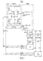
- the converter device DAC represented in Fig. 1 has a signal input IN1, a reference signal input IN2, and a difference output with output terminals OUT11 and OUT12 and includes a main circuit, comprising the series connection of a conversion circuit CC1 and a lowpass filter LPF1, and a closed loop control circuit which is coupled with CC1 and comprises the series connection of a conversion circuit CC2, a lowpass filter LPF2, a measurement and comparator circuit COMP2 and a signal generator or pulse width modulator PWM2.
- the converter device operates with the supply voltages VDD, VSS and VAG which are nominally equal to 2.5 volts, -2.5 Volts and 0 Volt respectively.
- VDD, VSS and VAG are nominally equal to 2.5 volts, -2.5 Volts and 0 Volt respectively.
- VAG is a fixed voltage, but VDD and VSS may change over ⁇ 37 milli-Volts.
- the converter device serves for converting a digital binary Pulse Density Modulated, or PDM, input signal with a bit frequency of 15.36 Megabit;sec to an analog output signal with a bandwidth of 120 kHz.
- PDM Pulse Density Modulated
- This PDM signal is for instance represented in Fig.
- the conversion circuit CC1 of the main circuit has the signal input IN1, two control of clock inputs CL11 and CL12 which are connected to respective outputs CL1 and CL2 of the regulating circuit and a difference output with two output terminals 011 and 012. In their turn these terminals are connected to like named inputs of the 120 kHz lowpass filter LPF1 constituted by two series resistances R11 and R12 and a shunt capacitator C1, the output terminals OUT11 and OUT12 of these resistances constituting the difference output of the device.
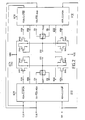
- the conversion circuit CC1 is represented in detail in Fig. 2 and includes two similar conversing circuits CC11 and CC12 which are represented in the left hand side and in the right hand side of the figure respectively.
- the converting circuit CC11 includes a logic circuit LC11 with signal IN1 and clock inputs CL11 and CL12 and with gate outputs PDA, PDA .
- XA, XA , NDA and NDA on which like named gating signals PDA.
- PDA , XA, XA , NDA and NDA are generated.
- the converting circuit CC1 moreover includes a switching circuit which is connected between VDD and VSS and which comprises the series connection of two electronic switches, i.e.
- PMOS transistor PM1 and NMOS transistor NM1 whose intercoupled drain electrodes constitute the output terminal 011 of the circuit.
- This terminal also constitutes the output of a third electronic switch, i.e. pass gate transistor PG1 whose input is connected to VAG and whose control electrodes are controlled by the gating signals XA and 5U .
- the drain electrode of each of the MOS transistors PM1 and NM1 is connected to the intercoupled source and drain electrodes of an associated compensation MOS transistor, i.e. PM3 and NM3.
- the gate electrodes of these transistors are controlled by means of the respective gating signals PDA and NDA which are phase-shifted over 180 degrees with respect to the gating signal PDA and NDA controlling the gate electrodes of PM1 and NM1 respectively.
- the converting circuit CC12 includes a logic circuit LC12 with signal input IN1 and clock inputs CL11 and CL12 and with gate outputs PDB, PDB , XB, XB , NDB, NDB as well as a switching circuit including the transistors PM2, PM4, NM2, NM4 and PG2 and having an output terminal 012.
- the logic circuit LC12 generates at its outputs the like named gating signals PDB, PDB , XB, XB , NDB and NDB controlling the last mentioned transistors.
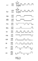
- gating signals appearing at the outputs of LC11 and LC12 and controlling the associated switching circuits may be represented by the following Boolean functions :
- each converting circuit such as CC11
- the levels VDD' and VSS with duration T of the PDM input signal are thus each converted to a plurality of output pulses with period T and of which the duration is equal to the duration of the pulses of the respective clock signals CL1 and CL2.
- the output signal 011 is considered then it follows from Fig. 3 that :
- each of the compensation transistors PM3/4 and NM3/4 is to eliminate spurious signals which would otherwise appear at the drain electrodes of PM.1/2, NM2/2 and therefore on the outputs 011 and 012 due to the presence of spurious capacitances between the electrodes of the transistor. This happens by generating spurious signals of opposite sign on these electrodes.
- the conversion circuit CC2 of the regulating circuit is the same as the conversion circuit CC1 and includes two converting circuits CC21 and CC22 (not shown) each with an input IN2 which is now used as a reference signal input. with two clock inputs CL21 and CL22 connected to the respective outputs CL1 and CL2, and with a respective output 021 and 022. These outputs are in their turn connected to like named inputs of the 120 kHz lowpass filter LPF2 which is identical to LPF1 and which has output terminals OUT21 and OUT22 of a difference output.
- This filter includes the series resistance R21 and R22 and the shunt capacitor C2.
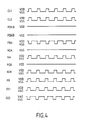
- the gating signals NDA, NDA and PDB. PDB block the transistors NM1,3 and PM24 respectively, whilst the remaining gating signals control the transistor pairs PM1 3 and NM2/4 and the passgate transistors PG1 and PG2 (all not shown) of CC2 insuch a way that the shown signals 021 and 022 appear at the outputs 021 and 022 thereof.
- the signal 021 only consists of a continuous series of positively directed first pulses with a duration T1 determined by CL1 and an amplitude comprised between VDD and VAG. It is therefore a positively directed binary signal or, in other words, a ternary signal wth a maximum positive value which is independent from VSS.
- the signal 022 only consists of a continuous series of negatively directed second pulses with a duration T2 determined by CL2 and an amplitude comprised between VAG and VSS. It is therefore a negatively directed binary signal or, in other words, a ternary signal with a maximum negative value which is independent from VDD.
- auxiliary signals OUT21 and OUT22 are supplied to the measurement or comparator circuit COMP2 including two operational amplifiers OA21 and OA22 which operated as comparators.
- the minus input of OA21 is connected to the output terminal OUT21 of LPF2, whilst the reference voltage VR is connected to its plus input.
- the reference voltage -VR is applied to the minus input of OA22, whilst its plus input is coupled to the output terminal OUT22 of LPF2, so that the measurement signal V22 at the like named output terminal V22 of OA22 increases;decreases when the auxiliary signal on OUT22 increases decreases.
- the outputs V21 and V22 of OA21 and OA22 are connected to like named inputs of two clocked pulse width modulator circuits PWMC21 and PWMC22 forming part of the clock signal generator or pulse width modulator PWM2 and having outputs CL1 and CL2. Because both these circuits are identical only PWMC21 is represented in detail.
- This clocked pulse width modulator circuit PWMC21 includes three branches connected between VDD and VSS : two of them each consist of the series connection of a PMOS transistor and an NMOS transistor, i.e. PMS, NM5 and PM6, NM6 and the third consists of the series connection of PMOS transistor PM7 and capacitor C, the junction point A of PM7 and C being connected to the joined drain electrodes of PM5 and NM5 as well as to the joined gate electrodes of PM6 and NM6.
- the drain electrodes of PM6 and NM6 and the gate electrode of PM7 are interconnected and constitute the output CL1 of PWMC21.
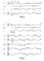
- the operation of the pulse width modulator circuit PWMC21 is as follows when it is assumed that the lower or higher measurement signal V21 shown in Fig. 5 or 6 and provided by the comparator circuit COMP2 is applied to the gate of transistor PM5. whilst the shown clock signal C1 with period with period T is supplied to the gate of NM5.
- the positively directed pulses of CL transistor NM5 becomes conductive due to which the possibly charged capacitor C is discharged towards VSS. Because point A is brought at this voltage VSS transistor PM6 becomes conductive due to which VDD appears at the output CL1 and NM6 is blocked, i.e. the invertor PM6, NM6 is triggered into another position. Also PM7 is then blocked.
- the surface of each of the (positively directed) first pulses of the signal 021 have their nominal value.
- the auxiliary signal OUT21 and the measurement signal V21 have their nominal value and also the pulses of CL1 have their nominal duration T1.
- this duration or width is dependent on the resistance of PM5 which is determined by the amplitude of the error signal V21.
- the clock signal CL1 is a signal which is pulse width modulated in function of the deviation of VDD from its nominal value.
- the pulses of the clock signal CL1 have a longer duration than their nominal duration because the measurement signal V21 has a higher value than its nominal value.
- transistor PM5 becomes less conductive and thus constitutes a higher resistance due to which the capacitor C in the circuit PWMC21 is charged more slowly than in the nominal case.
- the duration of the pulses of the clock signal CL1 becomes larger, as indicated in Fig. 6.
- the duration of the positively directed pulses of the signal 011 become larger due to which the average value of this signal increases. This average increases until the measurement signal V21 is again zero, at which moment the effect of the decrease of VDD is eliminated.
- the same regulator circuit in a similar way the same regulator circuit, but now via OA22 and PWMC21, regulates the width T2 of the pulses of the clock signal CL2 in function of VSS so that the surface of the pulses of the intermediate clock signal 022, and therefore of the negatively directed pulses of 021, is independent from a variation of VSS and/or whatever other parameter.
- the thus regulated clock signals CL1 and CL2 are supplied to the circuit CC1 then the operation of this circuit is independent from a variation of VDD and/or VSS and/or whatever other parameter because - as described above - such a variation is compensated by a variation of the width of the positively and/or negatively directed pulses of 011 and 012.
- Fig. 7 representing an integrator and comparator circuit to be substituted for the filter circuit LPF2 and the comparator circuit COMP2 of Fig. 1.
- the advantage of this replacement circuit is that it has a smaller number of poles than LPF2/COMP2 so that it is easier to make it stable.
- the terminals 021 and 022 are connected through resistances R21 and R22 with the minus and plus terminals of respective operational amplifiers OA21 and OA22.
- no capacitor C2 is connected between these terminals, but each of the amplifiers OA21 and OA22 is provided with a respective integration capacitor C3 and C4 which is connected between the minus terminal and the output terminal.
- the reference voltage -VR is not directly connected to the minus terminal of OA22, but it is connected to this minus terminal via the resistance R3.
- -VR is connected to the plus terminal of OA22 via capacitor C5.
Landscapes
- Analogue/Digital Conversion (AREA)
- Glass Compositions (AREA)
- Ultra Sonic Daignosis Equipment (AREA)
- Polarising Elements (AREA)
- Control Of Motors That Do Not Use Commutators (AREA)
- Amplifiers (AREA)
- Epoxy Resins (AREA)
- Oscillators With Electromechanical Resonators (AREA)
- Confectionery (AREA)
- External Artificial Organs (AREA)
- Dc-Dc Converters (AREA)
Priority Applications (1)
| Application Number | Priority Date | Filing Date | Title |
|---|---|---|---|
| AT88202028T ATE103433T1 (de) | 1987-09-30 | 1988-09-16 | Umsetzungsvorrichtung. |
Applications Claiming Priority (2)
| Application Number | Priority Date | Filing Date | Title |
|---|---|---|---|
| BE8701063 | 1987-09-30 | ||
| BE8701063A BE1000934A7 (nl) | 1987-09-30 | 1987-09-30 | Omvormingsinrichting. |
Publications (3)
| Publication Number | Publication Date |
|---|---|
| EP0310170A2 true EP0310170A2 (de) | 1989-04-05 |
| EP0310170A3 EP0310170A3 (en) | 1990-05-23 |
| EP0310170B1 EP0310170B1 (de) | 1994-03-23 |
Family
ID=3882871
Family Applications (1)
| Application Number | Title | Priority Date | Filing Date |
|---|---|---|---|
| EP88202028A Expired - Lifetime EP0310170B1 (de) | 1987-09-30 | 1988-09-16 | Umsetzungsvorrichtung |
Country Status (7)
| Country | Link |
|---|---|
| EP (1) | EP0310170B1 (de) |
| AT (1) | ATE103433T1 (de) |
| AU (1) | AU606212B2 (de) |
| BE (1) | BE1000934A7 (de) |
| DE (1) | DE3888615T2 (de) |
| ES (1) | ES2053710T3 (de) |
| NO (1) | NO180135C (de) |
Cited By (3)
| Publication number | Priority date | Publication date | Assignee | Title |
|---|---|---|---|---|
| EP0858162A3 (de) * | 1997-02-05 | 1999-07-28 | President of Hiroshima University | Schaltung zur Verarbeitung von pulsbreitenmodulierten Signalen |
| JP2004194335A (ja) * | 2002-12-11 | 2004-07-08 | Dialog Semiconductor Gmbh | D級増幅器の重心補償 |
| JP2004194334A (ja) * | 2002-12-11 | 2004-07-08 | Dialog Semiconductor Gmbh | Pdmd級増幅器の線形化 |
Family Cites Families (2)
| Publication number | Priority date | Publication date | Assignee | Title |
|---|---|---|---|---|
| IL42784A (en) * | 1972-08-09 | 1975-12-31 | Greatbatch W Ltd | Constant energy pulse generator |
| US3867650A (en) * | 1973-12-03 | 1975-02-18 | Bell Telephone Labor Inc | Compound transistor connection loading for a current |
-
1987
- 1987-09-30 BE BE8701063A patent/BE1000934A7/nl not_active IP Right Cessation
-
1988
- 1988-09-16 ES ES88202028T patent/ES2053710T3/es not_active Expired - Lifetime
- 1988-09-16 EP EP88202028A patent/EP0310170B1/de not_active Expired - Lifetime
- 1988-09-16 AT AT88202028T patent/ATE103433T1/de not_active IP Right Cessation
- 1988-09-16 DE DE3888615T patent/DE3888615T2/de not_active Expired - Fee Related
- 1988-09-20 NO NO884161A patent/NO180135C/no not_active IP Right Cessation
- 1988-09-26 AU AU22792/88A patent/AU606212B2/en not_active Ceased
Cited By (4)
| Publication number | Priority date | Publication date | Assignee | Title |
|---|---|---|---|---|
| EP0858162A3 (de) * | 1997-02-05 | 1999-07-28 | President of Hiroshima University | Schaltung zur Verarbeitung von pulsbreitenmodulierten Signalen |
| US6157672A (en) * | 1997-02-05 | 2000-12-05 | President Of Hiroshima University | Pulse modulation operation circuit |
| JP2004194335A (ja) * | 2002-12-11 | 2004-07-08 | Dialog Semiconductor Gmbh | D級増幅器の重心補償 |
| JP2004194334A (ja) * | 2002-12-11 | 2004-07-08 | Dialog Semiconductor Gmbh | Pdmd級増幅器の線形化 |
Also Published As
| Publication number | Publication date |
|---|---|
| ATE103433T1 (de) | 1994-04-15 |
| BE1000934A7 (nl) | 1989-05-16 |
| NO884161D0 (no) | 1988-09-20 |
| EP0310170A3 (en) | 1990-05-23 |
| NO180135C (no) | 1997-02-19 |
| ES2053710T3 (es) | 1994-08-01 |
| NO180135B (no) | 1996-11-11 |
| EP0310170B1 (de) | 1994-03-23 |
| DE3888615T2 (de) | 1994-07-21 |
| DE3888615D1 (de) | 1994-04-28 |
| AU2279288A (en) | 1989-04-06 |
| AU606212B2 (en) | 1991-01-31 |
| NO884161L (no) | 1989-03-31 |
Similar Documents
| Publication | Publication Date | Title |
|---|---|---|
| US4356450A (en) | Offset compensating circuit for operational amplifier | |
| US4598270A (en) | Precision integrating analog-to-digital converter system | |
| US4994730A (en) | Current source circuit with complementary current mirrors | |
| JPH07307620A (ja) | ボトム検出回路 | |
| US4254376A (en) | Apparatus for measuring the electric power or energy in an A-C network | |
| US4585951A (en) | Precision triangle waveform generator | |
| EP0310170B1 (de) | Umsetzungsvorrichtung | |
| US4527133A (en) | Self-balancing current sources for a delta modulator | |
| US4965867A (en) | Offset compensation circuit | |
| US3889197A (en) | Timer apparatus utilizing operational amplifier integrating means | |
| JPH0577206B2 (de) | ||
| EP0219937A3 (de) | Gesteuerter ECL-Referenzgenerator | |
| EP0670499B1 (de) | Spannungs-Frequenzwandler | |
| JPS61242411A (ja) | バイアス設定回路 | |
| US4717848A (en) | Electronic circuits and signal generator using them | |
| US4588984A (en) | Clocked precision integrating analog-to-digital converter system | |
| NO843682L (no) | Tellepulsgenerator. | |
| JPH1032926A (ja) | 電源電圧制御回路 | |
| EP0193244A2 (de) | Polaritätsumkehrungsschaltung | |
| SU1041984A1 (ru) | Преобразователь разности напр жений | |
| JPH05275995A (ja) | 帰還形パルス幅変調回路 | |
| KR0180464B1 (ko) | 인덱스 펄스 발생회로 | |
| US6087876A (en) | Time delay generator and method | |
| SU1150739A1 (ru) | Автогенератор пилообразного напр жени | |
| JPH01149071A (ja) | 半導体レーザ制御装置 |
Legal Events
| Date | Code | Title | Description |
|---|---|---|---|
| PUAI | Public reference made under article 153(3) epc to a published international application that has entered the european phase |
Free format text: ORIGINAL CODE: 0009012 |
|
| AK | Designated contracting states |
Kind code of ref document: A2 Designated state(s): AT BE CH DE ES FR GB IT LI NL SE |
|
| PUAL | Search report despatched |
Free format text: ORIGINAL CODE: 0009013 |
|
| AK | Designated contracting states |
Kind code of ref document: A3 Designated state(s): AT BE CH DE ES FR GB IT LI NL SE |
|
| 17P | Request for examination filed |
Effective date: 19901117 |
|
| 17Q | First examination report despatched |
Effective date: 19920710 |
|
| GRAA | (expected) grant |
Free format text: ORIGINAL CODE: 0009210 |
|
| AK | Designated contracting states |
Kind code of ref document: B1 Designated state(s): AT BE CH DE ES FR GB IT LI NL SE |
|
| REF | Corresponds to: |
Ref document number: 103433 Country of ref document: AT Date of ref document: 19940415 Kind code of ref document: T |
|
| ITF | It: translation for a ep patent filed | ||
| REF | Corresponds to: |
Ref document number: 3888615 Country of ref document: DE Date of ref document: 19940428 |
|
| ET | Fr: translation filed | ||
| REG | Reference to a national code |
Ref country code: ES Ref legal event code: FG2A Ref document number: 2053710 Country of ref document: ES Kind code of ref document: T3 |
|
| PLBE | No opposition filed within time limit |
Free format text: ORIGINAL CODE: 0009261 |
|
| STAA | Information on the status of an ep patent application or granted ep patent |
Free format text: STATUS: NO OPPOSITION FILED WITHIN TIME LIMIT |
|
| EAL | Se: european patent in force in sweden |
Ref document number: 88202028.2 |
|
| 26N | No opposition filed | ||
| PGFP | Annual fee paid to national office [announced via postgrant information from national office to epo] |
Ref country code: GB Payment date: 20010814 Year of fee payment: 14 |
|
| PGFP | Annual fee paid to national office [announced via postgrant information from national office to epo] |
Ref country code: CH Payment date: 20010816 Year of fee payment: 14 |
|
| PGFP | Annual fee paid to national office [announced via postgrant information from national office to epo] |
Ref country code: AT Payment date: 20010824 Year of fee payment: 14 |
|
| PGFP | Annual fee paid to national office [announced via postgrant information from national office to epo] |
Ref country code: SE Payment date: 20010827 Year of fee payment: 14 Ref country code: NL Payment date: 20010827 Year of fee payment: 14 |
|
| PGFP | Annual fee paid to national office [announced via postgrant information from national office to epo] |
Ref country code: DE Payment date: 20010903 Year of fee payment: 14 |
|
| PGFP | Annual fee paid to national office [announced via postgrant information from national office to epo] |
Ref country code: FR Payment date: 20010904 Year of fee payment: 14 |
|
| PGFP | Annual fee paid to national office [announced via postgrant information from national office to epo] |
Ref country code: ES Payment date: 20010918 Year of fee payment: 14 |
|
| PGFP | Annual fee paid to national office [announced via postgrant information from national office to epo] |
Ref country code: BE Payment date: 20010919 Year of fee payment: 14 |
|
| REG | Reference to a national code |
Ref country code: GB Ref legal event code: IF02 |
|
| PG25 | Lapsed in a contracting state [announced via postgrant information from national office to epo] |
Ref country code: GB Free format text: LAPSE BECAUSE OF NON-PAYMENT OF DUE FEES Effective date: 20020916 Ref country code: AT Free format text: LAPSE BECAUSE OF NON-PAYMENT OF DUE FEES Effective date: 20020916 |
|
| PG25 | Lapsed in a contracting state [announced via postgrant information from national office to epo] |
Ref country code: SE Free format text: LAPSE BECAUSE OF NON-PAYMENT OF DUE FEES Effective date: 20020917 Ref country code: ES Free format text: LAPSE BECAUSE OF NON-PAYMENT OF DUE FEES Effective date: 20020917 |
|
| PG25 | Lapsed in a contracting state [announced via postgrant information from national office to epo] |
Ref country code: LI Free format text: LAPSE BECAUSE OF NON-PAYMENT OF DUE FEES Effective date: 20020930 Ref country code: CH Free format text: LAPSE BECAUSE OF NON-PAYMENT OF DUE FEES Effective date: 20020930 Ref country code: BE Free format text: LAPSE BECAUSE OF NON-PAYMENT OF DUE FEES Effective date: 20020930 |
|
| BERE | Be: lapsed |
Owner name: *ALCATEL BELL Effective date: 20020930 |
|
| PG25 | Lapsed in a contracting state [announced via postgrant information from national office to epo] |
Ref country code: NL Free format text: LAPSE BECAUSE OF NON-PAYMENT OF DUE FEES Effective date: 20030401 Ref country code: DE Free format text: LAPSE BECAUSE OF NON-PAYMENT OF DUE FEES Effective date: 20030401 |
|
| EUG | Se: european patent has lapsed | ||
| GBPC | Gb: european patent ceased through non-payment of renewal fee |
Effective date: 20020916 |
|
| REG | Reference to a national code |
Ref country code: CH Ref legal event code: PL |
|
| PG25 | Lapsed in a contracting state [announced via postgrant information from national office to epo] |
Ref country code: FR Free format text: LAPSE BECAUSE OF NON-PAYMENT OF DUE FEES Effective date: 20030603 |
|
| REG | Reference to a national code |
Ref country code: FR Ref legal event code: ST |
|
| REG | Reference to a national code |
Ref country code: ES Ref legal event code: FD2A Effective date: 20031011 |
|
| PG25 | Lapsed in a contracting state [announced via postgrant information from national office to epo] |
Ref country code: IT Free format text: LAPSE BECAUSE OF NON-PAYMENT OF DUE FEES;WARNING: LAPSES OF ITALIAN PATENTS WITH EFFECTIVE DATE BEFORE 2007 MAY HAVE OCCURRED AT ANY TIME BEFORE 2007. THE CORRECT EFFECTIVE DATE MAY BE DIFFERENT FROM THE ONE RECORDED. Effective date: 20050916 |