EP0312239A2 - Botschafts-Fifo-Puffersteuergerät - Google Patents
Botschafts-Fifo-Puffersteuergerät Download PDFInfo
- Publication number
- EP0312239A2 EP0312239A2 EP88309253A EP88309253A EP0312239A2 EP 0312239 A2 EP0312239 A2 EP 0312239A2 EP 88309253 A EP88309253 A EP 88309253A EP 88309253 A EP88309253 A EP 88309253A EP 0312239 A2 EP0312239 A2 EP 0312239A2
- Authority
- EP
- European Patent Office
- Prior art keywords
- signal
- output
- counter
- comparator
- logic
- Prior art date
- Legal status (The legal status is an assumption and is not a legal conclusion. Google has not performed a legal analysis and makes no representation as to the accuracy of the status listed.)
- Granted
Links
Images

Classifications
-
- G—PHYSICS
- G11—INFORMATION STORAGE
- G11C—STATIC STORES
- G11C7/00—Arrangements for writing information into, or reading information out from, a digital store
-
- G—PHYSICS
- G06—COMPUTING OR CALCULATING; COUNTING
- G06F—ELECTRIC DIGITAL DATA PROCESSING
- G06F5/00—Methods or arrangements for data conversion without changing the order or content of the data handled
- G06F5/06—Methods or arrangements for data conversion without changing the order or content of the data handled for changing the speed of data flow, i.e. speed regularising or timing, e.g. delay lines, FIFO buffers; over- or underrun control therefor
- G06F5/10—Methods or arrangements for data conversion without changing the order or content of the data handled for changing the speed of data flow, i.e. speed regularising or timing, e.g. delay lines, FIFO buffers; over- or underrun control therefor having a sequence of storage locations each being individually accessible for both enqueue and dequeue operations, e.g. using random access memory
- G06F5/12—Means for monitoring the fill level; Means for resolving contention, i.e. conflicts between simultaneous enqueue and dequeue operations
- G06F5/14—Means for monitoring the fill level; Means for resolving contention, i.e. conflicts between simultaneous enqueue and dequeue operations for overflow or underflow handling, e.g. full or empty flags
-
- G—PHYSICS
- G06—COMPUTING OR CALCULATING; COUNTING
- G06F—ELECTRIC DIGITAL DATA PROCESSING
- G06F2205/00—Indexing scheme relating to group G06F5/00; Methods or arrangements for data conversion without changing the order or content of the data handled
- G06F2205/06—Indexing scheme relating to groups G06F5/06 - G06F5/16
- G06F2205/062—Allowing rewriting or rereading data to or from the buffer
Definitions
- This invention relates generally to FIFO (First In First Out) memories, and more particularly to a control circuit for FIFO memories.
- FIFO First In First Out
- FIFO memories are well known.
- One type of FIFO memory consists of a random access memory (RAM) associated with control circuitry.
- the control circuitry is used to control the writing of data into the RAM and the reading of data from the RAM.
- the present invention is not unlike those of the prior art in that it uses two counters, but it additionally employs an extra bit in each counter that when used with appropriate logic circuitry produces status (or control) signals for the FIFO; i.e. empty or full.
- the operation of the present invention is in a "message" mode. In one embodiment the operation of the present invention provides the capability of re-writing a section of memory and of re-reading a section of memory.
- the present invention also does away with an up/down counter and its associated complexities.
- the present invention is a control circuit for a FIFO (first in first out) memory circuit for providing address information to a FIFO memory means, the control circuit comprising: a first means for providing a first binary signal; a second means for providing a second binary signal; a first storage means for selectively receiving and storing the output of the first means; second storage means for selectively receiving and storing the output of the second means; first comparator means for comparing the output of the first storage means with the output of the second means and producing a first control signal indicative of the comparison; and second comparator means for comparing the output of the second storage means with the output of the first means and producing a second control signal indicative of the comparison.
- the present invention is a control circuit for a FIFO (first in first out) memory circuit, the control circuit comprising: a first means for providing a first binary signal; a second means for providing a second binary signal; multiplexer means for receiving both the first signal and the second signal and selecting either the first or the second signal as its output; first comparator means for comparing the most significant bit of the first signal with the most significant bit of the second signal and producing a first control signal indicative of the comparison; second comparator means for comparing the bits of the first signal, less the most significant bit, with the bits of the second signal, less the most significant bit, and producing a second control signal indicative of the comparison; logic means, responsive to the first control signal and the second control signal, for producing an indicator signal indicative of the memory circuit being full or not.
- FIFO first in first out
- the present invention is a control circuit for a FIFO (first in first out) memory circuit for providing address information to a FIFO memory means, the control circuit comprising: first counter means for providing a first binary signal; second counter means for providing a second binary signal; multiplexer means for receiving both the first signal and the second signal and selecting either the first or second signa as its output; first storage means for selectively receiving and storing the output of the first counter means; second storage means for selectively receiving and storing the output of the second counter means; first bus means for applying the output of the first storage means to the first counter means; second bus means for applying the output of the second storage means to the second counter means; first comparator means for comparing the output of the first storage means with the output of the second counter means and producing a first control signal indicative of the comparison; and second comparator means for comparing the output of the second storage means with the output of the first counter means and producing a second control signal indicative of the comparison; whereby the output of the multiplexer, less the most significant bit, is
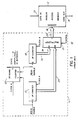
- Figure 1 depicts, in simplified form, a FIFO memory circuit 10 constructed according to known techniques.
- Circuit 10 comprises a FIFO control circuit 11 and a FIFO memory 12.
- FIFO memory 12 is a random access memory (RAM) having a data input port 13, a data output port 14, and an address port 16.
- RAM random access memory
- FIFO control circuit 11 comprises up counter 17, up counter 18, multiplexer 19, and up/down counter 20, interconnected as shown in Figure 1.
- Counters 17 and 18 are clocked by a clock signal A, as shown.
- Up counter 17 has a write enable input E as shown and up counter 18 has a read enable input E as shown.
- the output of counter 18, on bus 22, is applied to input port A of multiplexer 19; the output of counter 17, on bus 23, is applied to input port B of multiplexer 19.
- Output port C, of multiplexer 19, applies to bus 24 either the signal from input port A or input port B as selected by the control signal on control port 21.
- up counter 17 is a model 74F163
- up counter 18 is a model 74F163
- multiplexer 19 is a model 74F157
- Up/Down counter 20 is a model 74F199.
- a read enable signal (i.e. a logic 1) is applied to the E input of up counter 18.
- Counter 18 increases its count which is applied to multiplexer 19 via bus 22.
- the control signal applied to control input 21 of multiplexer 19 causes input port A of multiplexer 19 to be connected to output port C of multiplexer 19, and thus to bus 24 and then to address port 16 of RAM 12. Consequently, successive addresses are applied to RAM 12, and data stored in those addressed locations are applied in turn to data output port 14 of RAM 12.
- Up/Down Counter 20 is used to keep track of the state of RAM 12; i.e. is RAM 12 full, empty, or somewhere in between.
- the write enable signal from input E of counter 17 is applied to the up input terminal U of counter 20 (a signal applied here causes counter 20 to increase its count i.e. count up).
- the read enable signal from input E of counter 18 is applied to the down input terminal D of counter 20 (a signal applied here causes counter 20 to decrease its count i.e. count down).
- Output terminal 0 of counter 20 carries a count (i.e. number) indicative of the state of RAM 12.
- RAM 12 is empty then output 0 is zero; if RAM 12 is full then output 0 is FFF (hexadecimal) for this example; any number in between 0 and FFF (hex) indicates a measure of how full RAM 12 is. The larger the number, the fuller RAM 12 is.
- counter 20 started at zero when RAM 12 was empty.
- counter 20 counted up; when data was retrieved (read) from RAM 12 (as addressed by counter 18) counter 20 counted down.
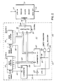
- FIG. 2 depicts, in simplified form, a FIFO memory circuit 110.
- Circuit 110 comprises FIFO control circuit 111 and FIFO memory 112.
- FIFO memory 112 is a random access memory (RAM) having a data input port 113, a data output port 114, and an address port 116.
- RAM random access memory
- FIFO control circuit 111 comprises write counter 117 (e.g. an up counter, model 74F163), read counter 118 (e.g. an up counter, model 74F163), multiplexer 119, (model 74F157), comparator 126 (model 74688), and comparator 127, interconnected as depicted in Figure 2.
- write counter 117 e.g. an up counter, model 74F163
- read counter 118 e.g. an up counter, model 74F163
- multiplexer 119 e.g. an up counter, model 74F163
- comparator 126 model 74688
- comparator 127 interconnected as depicted in Figure 2.
- Counters 117 and 118 are clocked by a clock signal A (4.096 MHz) as shown. Note that while counters 117 and 118 are depicted being clocked by a common clock A, they could be clocked by two different clocks. However, for ease of control (e.g. set-up time) is it preferred that counter 117 and 118 be clocked by two 180 degree out of phase signals from a common clock (e.g. A and A ).
- Write counter 117 has a write enable input E as shown and read counter 118 has a read enable input E as shown.
- the output of counter 118 less the most significant or overflow bit MSB, is applied to both input port A of multiplexer 119 and input port A of comparator 127, via bus 122.
- counter 117 less the most significant or overflow bit MSB, is applied to both input port B of multiplexer 119 and input port B of comparator 127, via bus 123. Note that if n bits are required to address RAM 112, then counter 117 is an (n + 1) bit counter and counter 118 is also an (n + 1) bit counter.
- Output port C, of multiplexer 119 applies to bus 124 either the signal from input port A or input port B as selected by the control signal on control port 121.
- the output signals 125 and 129 are applied to AND gates 133 and 134, respectively, as depicted in Figure 2.
- the other input of AND gates 133 and 134 is output signal 136 from output port 137 of comparator 127, as depicted in Figure 2.
- output signal 136 at port 137 is a logic 1; otherwise, output signal 136 is a logic 0.
- the output of AND gate 133 i.e. empty indication
- the output of AND gate 134 i.e. full indication, is a logic 0 signal.
- RAM 112 is only partially filled (e.g. 1K) when counter 117 is stopped and counter 118 is enabled to begin reading data from RAM 112.
- the output states of AND gates 133 and 134 remain unchanged (i.e. at logic 0 and 0 respectively) until the output of counter 118 equals the contents of counter 117.
- output signal 136 from comparator 127 becomes a logic 1 and consequently the output of AND gate 133 is a logic 1 and the output of AND gate 134 remains a logic 0.
- RAM 112 is empty because everything that has been stored in RAM 112 (i.e. under the control of counter 117) has been retrieved from RAM 112 (i.e. under the control of counter 118).
- counter 117 continues to increase its count and gets to the situation where its MSB is a logic 0 and its remaining bits are all logic 1's.
- bus 123 is carrying the highest possible address for RAM 112 (recall that counter 117 has one extra bit beyond that required to address RAM 112; i.e. if n bits are required to address RAM 112, then counter 117 has n + 1 bits).
- counter 117 changes to a logic 1 in its most significant bit MSB and the remainder of its bits are all logic 0.
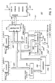
- FIG. 3 depicts, in simplified form, FIFO memory circuit 210 constructed according to the present invention.
- Circuit 210 comprises FIFO control circuit 211 and FIFO memory 212.
- FIFO memory 212 is a random access memory (RAM) having a data input port 213, a data output port 214, and an address port 216.
- RAM random access memory
- FIFO control circuit 211 comprises write counter 217 (e.g. an up counter, model 74F163), read counter 218 (e.g. an up counter, model 74F163), multiplexer 219 (model 74F157), comparator 241 (model 74688), comparator 248 (model 74688), comparator 251 (model 74688) write register 243, and read register 244, all interconnected as depicted in Figure 3.
- write counter 217 e.g. an up counter, model 74F163
- read counter 218 e.g. an up counter, model 74F163
- multiplexer 219 model 74F157
- comparator 241 model 74688
- comparator 248 model 74688
- comparator 251 model 74688
- Counters 217 and 218 are clocked by clock signal A, as shown.
- Write counter 217 has a write enable input E as shown and read counter 218 has a read enable input E as shown.
- the output of counter 218, including the most significant or overflow bit MSB is applied to input port A of multiplexer 219, to register 244, and to input port A of comparator 241, via bus 222 (note that the MSB is not required by multiplexer 219 or RAM 212).
- the output of counter 217, including the most significant or overflow bit MSB is applied to input port B of multiplexer 219, register 243, and to input port B of comparator 242, via bus 223 (note that the MSB is not required by multiplexer 219 or RAM 212).
- Output port C, of multiplexer 219, applies to bus 224 either the signal from input port A or input port B as selected by the control signal on control port 221.
- registers 243 and 244 are clocked by single event clock B and single event clock C, respectively.
- Single event clock B is a pulse that occurs when write counter 217 has stopped increasing (i.e. writing is finished) and the final count attained by counter 217 is to be stored in write register 243.
- Single event clock C is a pulse that occurs when read counter 212 has stopped increasing (i.e. reading is finished) and the final count attained by counter 218 is to be stored in read register 244.
- FIFO memory circuit 210 of Figure 3 operates in a "message" mode. That is, due to the fact that the values stored in registers 243 and 244 are not updated until the writing or reading, respectively, are completed, multi-increments are required before a status change (i.e. full or empty) is reflected on the indicators. In other words, a complete "message" must be written or read before a change of status occurs.
- write register 243 the contents of write register 243 are applied to the B input of comparator 241 while the output of read counter 218 is applied to the A input of comparator 241. If the signals at the A and B inputs of comparator 241 are both the same (i.e. equal) output signal 246, from comparator 241, is a logic 1 signal; otherwise it is a logic 0 signal.
- Signals 249 and 252 are applied to AND gate 253 as shown; the output of AND gate 253 is signal 247 as depicted in Figure 3 (this is of course also the output of comparator 242).
- RAM 212 is only partially filled (e.g. 1K) when counter 217 is stopped.
- register 243 is clocked by single event clock B and the signal on bus 223 (i.e. the count reached by counter 217) is stored in register 243.
- the A and B inputs of comparator 241 no longer carry equal signals and output signal 246 from comparator 241 becomes a logic 0 signal, indicating not empty.
- Output signal 247 from comparator 242 remains unchanged at a logic 0 indicating not full.
- register 244 is clocked by single event clock C and the signal on bus 222 (i.e. the count reached by counter 218) is stored in register 244.
- the A and B inputs of comparator 251 carry equal signals and output signal 247 from comparator 242 remains a logic 0 indicating not full.
- output signal 247 is a logic 0 signal indicating not full.
- counter 217 continues to increase its count and gets to the situation where its MSB is a logic 0 and its remaining bits are all logic 1's.
- bus 223 is carrying the highest possible address for RAM 212 (recall that counter 217 has one extra bit beyond that required to address RAM 212; i.e. if n bits are required to address RAM 212, then counter 217 has n + 1 bits).
- counter 217 changes to a logic 1 in its most significant bit MSB and the remainder of its bits are all logic 0.
- comparator 248 This results in the B and A inputs of comparator 248 being logic 1 and logic 0, respectively. Consequently, output signal 249 from comparator 248 is a logic 1 signal.
- the B input of comparator 251 is all logic 0's and the A input is 1K in binary. Consequently, output signal 252 from comparator 251 is a logic 0 signal (unequal inputs). This means that the inputs at AND gate 253 are a logic 1 and a logic 0 with the result that output signal 247 is a logic 0 indicating not full.
- RAM 212 is now full (signal 246 is a logic 0 and signal 247 is a logic 1) no more data can be written to RAM 212; data can only be read, as the next step.
- Output signal 247 does not change immediately because the input signals to comparator 242 have not yet changed (i.e. signal 247 remains a logic 1 indicating a full condition).
- Output signal 246 remains unchanged (at logic 0) until the output of counter 218 equals the contents of register 243. At that point in time, the two inputs to comparator 241 are equal and output signal 246 becomes a logic 1 signal indicating that RAM 212 is empty.
- register 244 is clocked by single event clock C and the signal on bus 222 (i.e. the count reached by counter 218) is stored in register 244.
- the A and B inputs of comparators 248 and 251 carry equal signals and output signal 247 becomes a logic 0 indicating not full.
- a circuit operated in the mode of the Figure 3 embodiment has the advantages that it is message oriented and therefore allows relatively smooth transfer of data that is message oriented.
- Figure 4 depicts, in simplified form, one preferred embodiment of a FIFO memory circuit 310 constructed according to the present invention.
- the embodiment of Figure 4 is similar to that depicted in Figure 3, but has the addition of bus 261 between register 244 and counter 218 and of bus 262 between register 243 and counter 217.
- buses 261 and 262 adds feedback between registers 243 and 244 and their corresponding counters 217 and 218, respectively, permits more control on the contents of FIFO memory 212.
- register 243 contains the starting count of counter 217 and register 243 does not store the final count of counter 217 until clocked by single event clock B. Consequently, by not providing the single event clock B signal, register 243 contains the starting count of counter 217; this count can then be inserted into counter 217 via bus 262. As a result, when counter 217 starts counting again, it will be starting at its earlier count and data now being stored in FIFO memory 212 will overwrite data that had already been stored there.
- register 244 contains the starting count of counter 218 and register 244 does not store the final count of counter 218 until clocked by single event clock C. Consequently, by not providing the single event clock C signal, register 244 contains the starting count of counter 218; this count can then be inserted into counter 218 via bus 261. As a result, when counter 218 starts counting again, it will be starting at its earlier count and data now being read (addressed) from FIFO memory 212 will be data that has already been read from memory 212.
- write register 243 is updated with the contents of write counter 217, thus "accepting" the message. If the controller (not shown) writing the message detects an integrity problem (e.g. parity) reloading write counter 217 with the contents of write register 243 "rejects" that message.
- an integrity problem e.g. parity
- read register 244 is normally updated from read counter 218, thus "purging" the message stored in FIFO memory 212. If, however, the receive controller (not shown) indicates an integrity problem (e.g. parity) it can reload counter 218 with the contents of read register 244 to "keep" the message in memory 212 for a retry (retransmission).
- an integrity problem e.g. parity
Landscapes
- Engineering & Computer Science (AREA)
- Theoretical Computer Science (AREA)
- Physics & Mathematics (AREA)
- General Engineering & Computer Science (AREA)
- General Physics & Mathematics (AREA)
- Communication Control (AREA)
- Synchronisation In Digital Transmission Systems (AREA)
- Multi Processors (AREA)
- Data Exchanges In Wide-Area Networks (AREA)
- Time-Division Multiplex Systems (AREA)
Applications Claiming Priority (2)
| Application Number | Priority Date | Filing Date | Title |
|---|---|---|---|
| CA000549274A CA1286421C (en) | 1987-10-14 | 1987-10-14 | Message fifo buffer controller |
| CA549274 | 1987-10-14 |
Publications (3)
| Publication Number | Publication Date |
|---|---|
| EP0312239A2 true EP0312239A2 (de) | 1989-04-19 |
| EP0312239A3 EP0312239A3 (de) | 1991-02-13 |
| EP0312239B1 EP0312239B1 (de) | 1996-05-08 |
Family
ID=4136650
Family Applications (1)
| Application Number | Title | Priority Date | Filing Date |
|---|---|---|---|
| EP88309253A Expired - Lifetime EP0312239B1 (de) | 1987-10-14 | 1988-10-05 | Botschafts-Fifo-Puffersteuergerät |
Country Status (7)
| Country | Link |
|---|---|
| US (1) | US4873666A (de) |
| EP (1) | EP0312239B1 (de) |
| JP (1) | JP2702181B2 (de) |
| KR (1) | KR890007284A (de) |
| CN (1) | CN1012396B (de) |
| CA (1) | CA1286421C (de) |
| DE (1) | DE3855274T2 (de) |
Cited By (5)
| Publication number | Priority date | Publication date | Assignee | Title |
|---|---|---|---|---|
| EP0534883A1 (de) * | 1991-09-16 | 1993-03-31 | International Business Machines Corporation | Verfahren und Gerät zur Synchronisierung der Auslese einer sequentiellen Mediumvorrichtung mit einer getrennten taktgesteuerten Vorrichtung |
| EP0577216A1 (de) * | 1992-07-01 | 1994-01-05 | Ampex Systems Corporation | Verzögerungssteuerung eines Tonempfängerpuffers in einer seriellen, digitalen Videoschnittstelle |
| EP0751458A1 (de) * | 1995-06-29 | 1997-01-02 | International Business Machines Corporation | Verfahren und Anordnung zur Überwachung von Ressourcenzuteilung innerhalb eines Prozessors |
| EP0758770A1 (de) * | 1995-08-14 | 1997-02-19 | Deutsche Thomson-Brandt Gmbh | Verfahren und Schaltungsanordnung zur Resynchronisation einer Speicherverwaltung |
| EP0768600A1 (de) * | 1995-10-13 | 1997-04-16 | Compaq Computer Corporation | Fifo-Puffer mit gesperrtem Austausch |
Families Citing this family (65)
| Publication number | Priority date | Publication date | Assignee | Title |
|---|---|---|---|---|
| JPH0778991B2 (ja) * | 1988-07-26 | 1995-08-23 | 株式会社東芝 | 半導体メモリ |
| US5255238A (en) * | 1988-09-08 | 1993-10-19 | Hitachi, Ltd. | First-in first-out semiconductor memory device |
| US5113398A (en) * | 1989-06-01 | 1992-05-12 | Shackleton System Drives Corporation | Self-healing data network and network node controller |
| US5084841A (en) * | 1989-08-14 | 1992-01-28 | Texas Instruments Incorporated | Programmable status flag generator FIFO using gray code |
| US5283763A (en) * | 1989-09-21 | 1994-02-01 | Ncr Corporation | Memory control system and method |
| US5455913A (en) * | 1990-05-14 | 1995-10-03 | At&T Global Information Solutions Company | System and method for transferring data between independent busses |
| JPH0437904A (ja) * | 1990-06-01 | 1992-02-07 | Mitsubishi Electric Corp | カウンタ装置 |
| US5214607A (en) * | 1990-11-26 | 1993-05-25 | Ncr Corporation | Look-ahead FIFO byte count apparatus |
| US5255241A (en) * | 1991-05-20 | 1993-10-19 | Tandem Computers Incorporated | Apparatus for intelligent reduction of worst case power in memory systems |
| US5551054A (en) * | 1991-11-19 | 1996-08-27 | Adaptec, Inc. | Page mode buffer controller for transferring Nb byte pages between a host and buffer memory without interruption except for refresh |
| JP3049343B2 (ja) * | 1991-11-25 | 2000-06-05 | 安藤電気株式会社 | メモリ試験装置 |
| JP3057591B2 (ja) * | 1992-12-22 | 2000-06-26 | 富士通株式会社 | マルチプロセッサシステム |
| JP3229066B2 (ja) * | 1993-04-21 | 2001-11-12 | セイコーインスツルメンツ株式会社 | 半導体集積回路 |
| US5487049A (en) * | 1994-11-23 | 1996-01-23 | Samsung Semiconductor, Inc. | Page-in, burst-out FIFO |
| US5555214A (en) | 1995-11-08 | 1996-09-10 | Altera Corporation | Apparatus for serial reading and writing of random access memory arrays |
| US7266725B2 (en) | 2001-09-03 | 2007-09-04 | Pact Xpp Technologies Ag | Method for debugging reconfigurable architectures |
| US6003107A (en) * | 1996-09-10 | 1999-12-14 | Hewlett-Packard Company | Circuitry for providing external access to signals that are internal to an integrated circuit chip package |
| US5881224A (en) * | 1996-09-10 | 1999-03-09 | Hewlett-Packard Company | Apparatus and method for tracking events in a microprocessor that can retire more than one instruction during a clock cycle |
| US5867644A (en) * | 1996-09-10 | 1999-02-02 | Hewlett Packard Company | System and method for on-chip debug support and performance monitoring in a microprocessor |
| US5887003A (en) * | 1996-09-10 | 1999-03-23 | Hewlett-Packard Company | Apparatus and method for comparing a group of binary fields with an expected pattern to generate match results |
| US5974482A (en) * | 1996-09-20 | 1999-10-26 | Honeywell Inc. | Single port first-in-first-out (FIFO) device having overwrite protection and diagnostic capabilities |
| US5956476A (en) * | 1996-10-31 | 1999-09-21 | Hewlett Packard Company | Circuitry and method for detecting signal patterns on a bus using dynamically changing expected patterns |
| US5956477A (en) * | 1996-11-25 | 1999-09-21 | Hewlett-Packard Company | Method for processing information in a microprocessor to facilitate debug and performance monitoring |
| US6009539A (en) * | 1996-11-27 | 1999-12-28 | Hewlett-Packard Company | Cross-triggering CPUs for enhanced test operations in a multi-CPU computer system |
| US5881217A (en) * | 1996-11-27 | 1999-03-09 | Hewlett-Packard Company | Input comparison circuitry and method for a programmable state machine |
| DE19654595A1 (de) | 1996-12-20 | 1998-07-02 | Pact Inf Tech Gmbh | I0- und Speicherbussystem für DFPs sowie Bausteinen mit zwei- oder mehrdimensionaler programmierbaren Zellstrukturen |
| US6542998B1 (en) | 1997-02-08 | 2003-04-01 | Pact Gmbh | Method of self-synchronization of configurable elements of a programmable module |
| US8686549B2 (en) * | 2001-09-03 | 2014-04-01 | Martin Vorbach | Reconfigurable elements |
| DE19861088A1 (de) | 1997-12-22 | 2000-02-10 | Pact Inf Tech Gmbh | Verfahren zur Reparatur von integrierten Schaltkreisen |
| KR100301653B1 (ko) * | 1998-08-14 | 2001-09-06 | 김영환 | 고속 엠티 플래그 발생기 |
| US6374370B1 (en) | 1998-10-30 | 2002-04-16 | Hewlett-Packard Company | Method and system for flexible control of BIST registers based upon on-chip events |
| US7003660B2 (en) | 2000-06-13 | 2006-02-21 | Pact Xpp Technologies Ag | Pipeline configuration unit protocols and communication |
| DE10081643D2 (de) * | 1999-06-10 | 2002-05-29 | Pact Inf Tech Gmbh | Sequenz-Partitionierung auf Zellstrukturen |
| US8058899B2 (en) | 2000-10-06 | 2011-11-15 | Martin Vorbach | Logic cell array and bus system |
| US7444531B2 (en) | 2001-03-05 | 2008-10-28 | Pact Xpp Technologies Ag | Methods and devices for treating and processing data |
| US9037807B2 (en) | 2001-03-05 | 2015-05-19 | Pact Xpp Technologies Ag | Processor arrangement on a chip including data processing, memory, and interface elements |
| US7844796B2 (en) | 2001-03-05 | 2010-11-30 | Martin Vorbach | Data processing device and method |
| US7996827B2 (en) | 2001-08-16 | 2011-08-09 | Martin Vorbach | Method for the translation of programs for reconfigurable architectures |
| US7434191B2 (en) | 2001-09-03 | 2008-10-07 | Pact Xpp Technologies Ag | Router |
| US8686475B2 (en) * | 2001-09-19 | 2014-04-01 | Pact Xpp Technologies Ag | Reconfigurable elements |
| CN1585924B (zh) * | 2001-11-13 | 2010-05-26 | Nxp股份有限公司 | 使用信号量进行fifo通信的方法和设备及计算机系统 |
| AU2003208266A1 (en) | 2002-01-19 | 2003-07-30 | Pact Xpp Technologies Ag | Reconfigurable processor |
| WO2003071432A2 (de) | 2002-02-18 | 2003-08-28 | Pact Xpp Technologies Ag | Bussysteme und rekonfigurationsverfahren |
| US20110161977A1 (en) * | 2002-03-21 | 2011-06-30 | Martin Vorbach | Method and device for data processing |
| US8914590B2 (en) | 2002-08-07 | 2014-12-16 | Pact Xpp Technologies Ag | Data processing method and device |
| CN100437466C (zh) * | 2002-06-07 | 2008-11-26 | Nxp股份有限公司 | 向/从fifo存储器读取/写入数据单元的设备和方法 |
| US7477649B2 (en) * | 2002-07-17 | 2009-01-13 | Lsi Corporation | Active FIFO threshold adjustment |
| US7657861B2 (en) | 2002-08-07 | 2010-02-02 | Pact Xpp Technologies Ag | Method and device for processing data |
| AU2003286131A1 (en) | 2002-08-07 | 2004-03-19 | Pact Xpp Technologies Ag | Method and device for processing data |
| WO2004038599A1 (de) | 2002-09-06 | 2004-05-06 | Pact Xpp Technologies Ag | Rekonfigurierbare sequenzerstruktur |
| JP2004246979A (ja) * | 2003-02-14 | 2004-09-02 | Fujitsu Ltd | 半導体試験回路、半導体記憶装置および半導体試験方法 |
| JP4700611B2 (ja) | 2003-08-28 | 2011-06-15 | ペーアーツェーテー イクスペーペー テクノロジーズ アクチエンゲゼルシャフト | データ処理装置およびデータ処理方法 |
| CN100396052C (zh) * | 2004-03-12 | 2008-06-18 | 华为技术有限公司 | 高可靠性的先入先出存储器及其实现方法 |
| US7447812B1 (en) | 2004-03-23 | 2008-11-04 | Integrated Device Technology, Inc. | Multi-queue FIFO memory devices that support flow-through of write and read counter updates using multi-port flag counter register files |
| US7523232B2 (en) * | 2004-07-26 | 2009-04-21 | Integrated Device Technology, Inc. | Mark/re-read and mark/re-write operations in a multi-queue first-in first-out memory system |
| US7870310B2 (en) * | 2004-07-26 | 2011-01-11 | Integrated Device Technology, Inc. | Multiple counters to relieve flag restriction in a multi-queue first-in first-out memory system |
| US7805552B2 (en) | 2004-07-26 | 2010-09-28 | Integrated Device Technology, Inc. | Partial packet write and write data filtering in a multi-queue first-in first-out memory system |
| US8230174B2 (en) * | 2004-07-26 | 2012-07-24 | Integrated Device Technology, Inc. | Multi-queue address generator for start and end addresses in a multi-queue first-in first-out memory system |
| US20060155940A1 (en) | 2005-01-10 | 2006-07-13 | Mario Au | Multi-queue FIFO memory systems that utilize read chip select and device identification codes to control one-at-a-time bus access between selected FIFO memory chips |
| WO2007063858A1 (ja) * | 2005-12-02 | 2007-06-07 | Matsushita Electric Industrial Co., Ltd. | バッファ制御装置およびバッファメモリ |
| WO2007082730A1 (de) | 2006-01-18 | 2007-07-26 | Pact Xpp Technologies Ag | Hardwaredefinitionsverfahren |
| JP2011503733A (ja) * | 2007-11-17 | 2011-01-27 | トーマス リヒター | リコンフィギュラブルな浮動小数点レベルおよびビットレベルのデータ処理ユニット |
| WO2009068014A2 (de) * | 2007-11-28 | 2009-06-04 | Pact Xpp Technologies Ag | Über datenverarbeitung |
| US8681526B2 (en) * | 2008-07-02 | 2014-03-25 | Cradle Ip, Llc | Size and retry programmable multi-synchronous FIFO |
| CN116107795B (zh) * | 2023-04-14 | 2023-07-14 | 苏州萨沙迈半导体有限公司 | 报错电路及芯片设备 |
Family Cites Families (13)
| Publication number | Priority date | Publication date | Assignee | Title |
|---|---|---|---|---|
| US3601809A (en) * | 1968-11-04 | 1971-08-24 | Univ Pennsylvania | Addressable list memory systems |
| US4163291A (en) * | 1975-10-15 | 1979-07-31 | Tokyo Shibaura Electric Co., Ltd. | Input-output control circuit for FIFO memory |
| DE2639895C2 (de) * | 1976-09-04 | 1983-06-16 | Nixdorf Computer Ag, 4790 Paderborn | Verfahren zur Übertragung von Informationssignalen aus einem Informationsspeicher in einem Datenkanal in Datenverarbeitungsanlagen und Einrichtung zur Durchführung des Verfahrens |
| US4171538A (en) * | 1978-01-23 | 1979-10-16 | Rockwell International Corporation | Elastic store slip circuit apparatus for preventing read and write operations interference |
| US4258418A (en) * | 1978-12-28 | 1981-03-24 | International Business Machines Corporation | Variable capacity data buffer system |
| JPS6057090B2 (ja) * | 1980-09-19 | 1985-12-13 | 株式会社日立製作所 | データ記憶装置およびそれを用いた処理装置 |
| US4378594A (en) * | 1980-10-24 | 1983-03-29 | Ncr Corporation | High speed to low speed data buffering means |
| JPS58191043A (ja) * | 1982-04-30 | 1983-11-08 | Nec Home Electronics Ltd | フア−ストイン・フア−ストアウトレジスタ制御回路 |
| US4507760A (en) * | 1982-08-13 | 1985-03-26 | At&T Bell Laboratories | First-in, first-out (FIFO) memory configuration for queue storage |
| FR2536200B1 (fr) * | 1982-11-15 | 1987-01-16 | Helen Andre | Unite de stockage temporaire de donnees organisee en file d'attente |
| US4592019A (en) * | 1983-08-31 | 1986-05-27 | At&T Bell Laboratories | Bus oriented LIFO/FIFO memory |
| JPS60262242A (ja) * | 1984-06-08 | 1985-12-25 | Matsushita Electric Ind Co Ltd | Fifo回路 |
| US4694426A (en) * | 1985-12-20 | 1987-09-15 | Ncr Corporation | Asynchronous FIFO status circuit |
-
1987
- 1987-10-14 CA CA000549274A patent/CA1286421C/en not_active Expired - Lifetime
- 1987-10-15 US US07/108,655 patent/US4873666A/en not_active Expired - Lifetime
-
1988
- 1988-10-05 DE DE3855274T patent/DE3855274T2/de not_active Expired - Fee Related
- 1988-10-05 EP EP88309253A patent/EP0312239B1/de not_active Expired - Lifetime
- 1988-10-11 JP JP63253939A patent/JP2702181B2/ja not_active Expired - Fee Related
- 1988-10-13 KR KR1019880013345A patent/KR890007284A/ko not_active Withdrawn
- 1988-10-14 CN CN88108439A patent/CN1012396B/zh not_active Expired
Cited By (8)
| Publication number | Priority date | Publication date | Assignee | Title |
|---|---|---|---|---|
| EP0534883A1 (de) * | 1991-09-16 | 1993-03-31 | International Business Machines Corporation | Verfahren und Gerät zur Synchronisierung der Auslese einer sequentiellen Mediumvorrichtung mit einer getrennten taktgesteuerten Vorrichtung |
| EP0577216A1 (de) * | 1992-07-01 | 1994-01-05 | Ampex Systems Corporation | Verzögerungssteuerung eines Tonempfängerpuffers in einer seriellen, digitalen Videoschnittstelle |
| US5323272A (en) * | 1992-07-01 | 1994-06-21 | Ampex Systems Corporation | Time delay control for serial digital video interface audio receiver buffer |
| EP0751458A1 (de) * | 1995-06-29 | 1997-01-02 | International Business Machines Corporation | Verfahren und Anordnung zur Überwachung von Ressourcenzuteilung innerhalb eines Prozessors |
| US5809268A (en) * | 1995-06-29 | 1998-09-15 | International Business Machines Corporation | Method and system for tracking resource allocation within a processor |
| EP0758770A1 (de) * | 1995-08-14 | 1997-02-19 | Deutsche Thomson-Brandt Gmbh | Verfahren und Schaltungsanordnung zur Resynchronisation einer Speicherverwaltung |
| EP0768600A1 (de) * | 1995-10-13 | 1997-04-16 | Compaq Computer Corporation | Fifo-Puffer mit gesperrtem Austausch |
| US5717954A (en) * | 1995-10-13 | 1998-02-10 | Compaq Computer Corporation | Locked exchange FIFO |
Also Published As
| Publication number | Publication date |
|---|---|
| CA1286421C (en) | 1991-07-16 |
| US4873666A (en) | 1989-10-10 |
| JP2702181B2 (ja) | 1998-01-21 |
| JPH01129323A (ja) | 1989-05-22 |
| EP0312239A3 (de) | 1991-02-13 |
| EP0312239B1 (de) | 1996-05-08 |
| DE3855274D1 (de) | 1996-06-13 |
| KR890007284A (ko) | 1989-06-19 |
| CN1035382A (zh) | 1989-09-06 |
| DE3855274T2 (de) | 1996-09-19 |
| CN1012396B (zh) | 1991-04-17 |
Similar Documents
| Publication | Publication Date | Title |
|---|---|---|
| US4873666A (en) | Message FIFO buffer controller | |
| US4873667A (en) | FIFO buffer controller | |
| US5097442A (en) | Programmable depth first-in, first-out memory | |
| US4486854A (en) | First-in, first-out memory system | |
| US5305253A (en) | Zero fall-through time asynchronous fifo buffer with nonambiguous empty-full resolution | |
| US5587953A (en) | First-in-first-out buffer memory | |
| US4873671A (en) | Sequential read access of serial memories with a user defined starting address | |
| US4899307A (en) | Stack with unary encoded stack pointer | |
| US5497478A (en) | Memory access system and method modifying a memory interleaving scheme so that data can be read in any sequence without inserting wait cycles | |
| JPH03130983A (ja) | パイプラインシリアルメモリ及びそのパイプラインの方法 | |
| EP0554209B1 (de) | Direktspeicherzugriffssteuerung | |
| US5555380A (en) | Data transfer system with buffer request including block length to update the buffer pointer prior to transferring of the block | |
| US4922457A (en) | Serial access memory system provided with improved cascade buffer circuit | |
| EP0057096A2 (de) | Informationsverarbeitungsanlage | |
| US4970679A (en) | Pulse input apparatus | |
| US5214777A (en) | High speed read/modify/write memory system and method | |
| JPS60245062A (ja) | デ−タ転送装置 | |
| US6374313B1 (en) | FIFO and method of operating same which inhibits output transitions when the last cell is read or when the FIFO is erased | |
| US5396611A (en) | Microprocessor use in in-circuit emulator having function of discriminating user's space and in-circuit emulator space | |
| US4584619A (en) | Programmable servo pattern generator | |
| JP3777047B2 (ja) | フラッシュメモリ装置の消去方法 | |
| SU1509871A1 (ru) | Устройство дл сортировки информации | |
| GB2145546A (en) | Magnetic bubble memory system | |
| JPH03100851A (ja) | 先入れ先出し記憶装置 | |
| JPH0628204A (ja) | レジスタ保護回路 |
Legal Events
| Date | Code | Title | Description |
|---|---|---|---|
| PUAI | Public reference made under article 153(3) epc to a published international application that has entered the european phase |
Free format text: ORIGINAL CODE: 0009012 |
|
| AK | Designated contracting states |
Kind code of ref document: A2 Designated state(s): DE FR GB IT NL SE |
|
| PUAL | Search report despatched |
Free format text: ORIGINAL CODE: 0009013 |
|
| AK | Designated contracting states |
Kind code of ref document: A3 Designated state(s): DE FR GB IT NL SE |
|
| 17P | Request for examination filed |
Effective date: 19910415 |
|
| 17Q | First examination report despatched |
Effective date: 19940524 |
|
| RAP1 | Party data changed (applicant data changed or rights of an application transferred) |
Owner name: NORTHERN TELECOM LIMITED |
|
| GRAH | Despatch of communication of intention to grant a patent |
Free format text: ORIGINAL CODE: EPIDOS IGRA |
|
| GRAA | (expected) grant |
Free format text: ORIGINAL CODE: 0009210 |
|
| AK | Designated contracting states |
Kind code of ref document: B1 Designated state(s): DE FR GB IT NL SE |
|
| PG25 | Lapsed in a contracting state [announced via postgrant information from national office to epo] |
Ref country code: IT Free format text: LAPSE BECAUSE OF FAILURE TO SUBMIT A TRANSLATION OF THE DESCRIPTION OR TO PAY THE FEE WITHIN THE PRESCRIBED TIME-LIMIT;WARNING: LAPSES OF ITALIAN PATENTS WITH EFFECTIVE DATE BEFORE 2007 MAY HAVE OCCURRED AT ANY TIME BEFORE 2007. THE CORRECT EFFECTIVE DATE MAY BE DIFFERENT FROM THE ONE RECORDED. Effective date: 19960508 Ref country code: NL Free format text: LAPSE BECAUSE OF FAILURE TO SUBMIT A TRANSLATION OF THE DESCRIPTION OR TO PAY THE FEE WITHIN THE PRESCRIBED TIME-LIMIT Effective date: 19960508 |
|
| ET | Fr: translation filed | ||
| REF | Corresponds to: |
Ref document number: 3855274 Country of ref document: DE Date of ref document: 19960613 |
|
| PG25 | Lapsed in a contracting state [announced via postgrant information from national office to epo] |
Ref country code: SE Effective date: 19960808 |
|
| NLV1 | Nl: lapsed or annulled due to failure to fulfill the requirements of art. 29p and 29m of the patents act | ||
| PLBE | No opposition filed within time limit |
Free format text: ORIGINAL CODE: 0009261 |
|
| STAA | Information on the status of an ep patent application or granted ep patent |
Free format text: STATUS: NO OPPOSITION FILED WITHIN TIME LIMIT |
|
| 26N | No opposition filed | ||
| REG | Reference to a national code |
Ref country code: GB Ref legal event code: IF02 |
|
| REG | Reference to a national code |
Ref country code: FR Ref legal event code: CD |
|
| PGFP | Annual fee paid to national office [announced via postgrant information from national office to epo] |
Ref country code: GB Payment date: 20040915 Year of fee payment: 17 |
|
| PGFP | Annual fee paid to national office [announced via postgrant information from national office to epo] |
Ref country code: FR Payment date: 20041004 Year of fee payment: 17 |
|
| PGFP | Annual fee paid to national office [announced via postgrant information from national office to epo] |
Ref country code: DE Payment date: 20041029 Year of fee payment: 17 |
|
| PG25 | Lapsed in a contracting state [announced via postgrant information from national office to epo] |
Ref country code: GB Free format text: LAPSE BECAUSE OF NON-PAYMENT OF DUE FEES Effective date: 20051005 |
|
| PG25 | Lapsed in a contracting state [announced via postgrant information from national office to epo] |
Ref country code: DE Free format text: LAPSE BECAUSE OF NON-PAYMENT OF DUE FEES Effective date: 20060503 |
|
| GBPC | Gb: european patent ceased through non-payment of renewal fee |
Effective date: 20051005 |
|
| PG25 | Lapsed in a contracting state [announced via postgrant information from national office to epo] |
Ref country code: FR Free format text: LAPSE BECAUSE OF NON-PAYMENT OF DUE FEES Effective date: 20060630 |
|
| REG | Reference to a national code |
Ref country code: FR Ref legal event code: ST Effective date: 20060630 |