EP0314511A2 - Betriebsverfahren für EL-Paneele zur Alterung - Google Patents
Betriebsverfahren für EL-Paneele zur Alterung Download PDFInfo
- Publication number
- EP0314511A2 EP0314511A2 EP88310194A EP88310194A EP0314511A2 EP 0314511 A2 EP0314511 A2 EP 0314511A2 EP 88310194 A EP88310194 A EP 88310194A EP 88310194 A EP88310194 A EP 88310194A EP 0314511 A2 EP0314511 A2 EP 0314511A2
- Authority
- EP
- European Patent Office
- Prior art keywords
- voltage
- picture elements
- electrodes
- voltages
- negative
- Prior art date
- Legal status (The legal status is an assumption and is not a legal conclusion. Google has not performed a legal analysis and makes no representation as to the accuracy of the status listed.)
- Granted
Links
- 238000000034 method Methods 0.000 title claims abstract description 38
- 239000010409 thin film Substances 0.000 title claims abstract description 14
- 230000002431 foraging effect Effects 0.000 title claims abstract description 9
- 239000002184 metal Substances 0.000 claims abstract description 45
- 238000004020 luminiscence type Methods 0.000 claims abstract description 23
- 230000032683 aging Effects 0.000 claims abstract description 17
- 238000007667 floating Methods 0.000 claims abstract description 5
- 239000004020 conductor Substances 0.000 claims description 27
- 230000015556 catabolic process Effects 0.000 description 9
- 230000008878 coupling Effects 0.000 description 4
- 238000010168 coupling process Methods 0.000 description 4
- 238000005859 coupling reaction Methods 0.000 description 4
- 238000010586 diagram Methods 0.000 description 4
- 238000010276 construction Methods 0.000 description 3
- 229910052581 Si3N4 Inorganic materials 0.000 description 2
- 230000002159 abnormal effect Effects 0.000 description 2
- 230000001419 dependent effect Effects 0.000 description 2
- 230000003292 diminished effect Effects 0.000 description 2
- 239000013543 active substance Substances 0.000 description 1
- 230000000694 effects Effects 0.000 description 1
- 239000010408 film Substances 0.000 description 1
- 239000011521 glass Substances 0.000 description 1
- 230000001939 inductive effect Effects 0.000 description 1
- 238000009413 insulation Methods 0.000 description 1
- 230000007257 malfunction Effects 0.000 description 1
- 238000004519 manufacturing process Methods 0.000 description 1
- 238000002360 preparation method Methods 0.000 description 1
- 238000004544 sputter deposition Methods 0.000 description 1
- 238000006467 substitution reaction Methods 0.000 description 1
- 239000000758 substrate Substances 0.000 description 1
- 238000007738 vacuum evaporation Methods 0.000 description 1
Images
Classifications
-
- G—PHYSICS
- G09—EDUCATION; CRYPTOGRAPHY; DISPLAY; ADVERTISING; SEALS
- G09G—ARRANGEMENTS OR CIRCUITS FOR CONTROL OF INDICATING DEVICES USING STATIC MEANS TO PRESENT VARIABLE INFORMATION
- G09G3/00—Control arrangements or circuits, of interest only in connection with visual indicators other than cathode-ray tubes
- G09G3/006—Electronic inspection or testing of displays and display drivers, e.g. of LED or LCD displays
Definitions
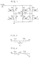
- the aging drive method comprises a first to a fourth field.
- a first voltage VD of positive polarity lower than luminescence start voltage is applied across the odd-numbered metal electrodes 6A, 6A,.. and the transparent electrodes 2, 2,... and across the even-numbered metal electrodes 6B, 6B,... and the transparent electrodes 2, 2,....
- a second voltage VD is applied across the odd-numbered metal electrodes 6A, 6A,... and the even-numbered metal electrodes 6B, 6B,... while holding the transparent electrodes 2, 2,... in floating state to cause the picture elements ELA to luminesce by the application of voltage of positive polarity to the transparent electrodes.
- the first field by be followed by the second, fourth and third fields in this order, or by the third, second and fourth fields, or by the third, fourth and second fields, or by the fourth, second and third fields, or by the fourth, third and second fields in the order mentioned.
Landscapes
- Engineering & Computer Science (AREA)
- Physics & Mathematics (AREA)
- Computer Hardware Design (AREA)
- General Physics & Mathematics (AREA)
- Theoretical Computer Science (AREA)
- Electroluminescent Light Sources (AREA)
- Control Of Indicators Other Than Cathode Ray Tubes (AREA)
Applications Claiming Priority (2)
| Application Number | Priority Date | Filing Date | Title |
|---|---|---|---|
| JP274983/87 | 1987-10-30 | ||
| JP62274983A JPH01117296A (ja) | 1987-10-30 | 1987-10-30 | 薄膜elパネルのエージング駆動方法 |
Publications (3)
| Publication Number | Publication Date |
|---|---|
| EP0314511A2 true EP0314511A2 (de) | 1989-05-03 |
| EP0314511A3 EP0314511A3 (en) | 1990-08-22 |
| EP0314511B1 EP0314511B1 (de) | 1993-12-22 |
Family
ID=17549277
Family Applications (1)
| Application Number | Title | Priority Date | Filing Date |
|---|---|---|---|
| EP88310194A Expired - Lifetime EP0314511B1 (de) | 1987-10-30 | 1988-10-28 | Betriebsverfahren für EL-Paneele zur Alterung |
Country Status (4)
| Country | Link |
|---|---|
| US (1) | US4949019A (de) |
| EP (1) | EP0314511B1 (de) |
| JP (1) | JPH01117296A (de) |
| DE (1) | DE3886503T2 (de) |
Families Citing this family (6)
| Publication number | Priority date | Publication date | Assignee | Title |
|---|---|---|---|---|
| US5235253A (en) * | 1990-11-27 | 1993-08-10 | Fuji Xerox Co., Ltd. | Thin-film electroluminescent device drive circuit |
| US6802752B1 (en) * | 1993-12-27 | 2004-10-12 | Canon Kabushiki Kaisha | Method of manufacturing electron emitting device |
| CA2299957C (en) * | 1993-12-27 | 2003-04-29 | Canon Kabushiki Kaisha | Electron-emitting device and method of manufacturing the same as well as electron source and image-forming apparatus |
| JP2002091387A (ja) * | 2000-09-13 | 2002-03-27 | Kawasaki Microelectronics Kk | Lcdドライバ |
| TW586334B (en) | 2001-09-10 | 2004-05-01 | Matsushita Electric Industrial Co Ltd | Self-ballasted fluorescent lamp |
| JP4154215B2 (ja) * | 2002-11-12 | 2008-09-24 | オプトレックス株式会社 | 有機エレクトロルミネッセンス表示素子の製造方法 |
Family Cites Families (3)
| Publication number | Priority date | Publication date | Assignee | Title |
|---|---|---|---|---|
| JPS6041438B2 (ja) * | 1980-06-23 | 1985-09-17 | シャープ株式会社 | エレクトロルミネツセンス表示素子のエ−ジング方法 |
| US4818913A (en) * | 1981-07-31 | 1989-04-04 | Sharp Kabushiki Kaisha | Aging method for thin-film electroluminescent display panel |
| US4527096A (en) * | 1984-02-08 | 1985-07-02 | Timex Corporation | Drive circuit for capacitive electroluminescent panels |
-
1987
- 1987-10-30 JP JP62274983A patent/JPH01117296A/ja active Granted
-
1988
- 1988-10-28 EP EP88310194A patent/EP0314511B1/de not_active Expired - Lifetime
- 1988-10-28 US US07/264,085 patent/US4949019A/en not_active Expired - Lifetime
- 1988-10-28 DE DE3886503T patent/DE3886503T2/de not_active Expired - Fee Related
Also Published As
| Publication number | Publication date |
|---|---|
| JPH0460316B2 (de) | 1992-09-25 |
| EP0314511A3 (en) | 1990-08-22 |
| DE3886503T2 (de) | 1994-05-26 |
| DE3886503D1 (de) | 1994-02-03 |
| JPH01117296A (ja) | 1989-05-10 |
| EP0314511B1 (de) | 1993-12-22 |
| US4949019A (en) | 1990-08-14 |
Similar Documents
| Publication | Publication Date | Title |
|---|---|---|
| KR100224119B1 (ko) | 평면표시용 구동장치 | |
| EP0068630B1 (de) | Elektrolumineszierende Anzeigevorrichtung | |
| US5006838A (en) | Thin film EL display panel drive circuit | |
| JPH07109798B2 (ja) | 薄膜el表示装置の駆動回路 | |
| US4237456A (en) | Drive system for a thin-film EL display panel | |
| EP0314511B1 (de) | Betriebsverfahren für EL-Paneele zur Alterung | |
| JPH0118434B2 (de) | ||
| EP0381479A1 (de) | Verfahren und Vorrichtung zum Treiben kapazitiver Displayeinrichtungen | |
| JPH0572589B2 (de) | ||
| JPS63314594A (ja) | 薄膜elディスプレイユニットの駆動方法および駆動回路 | |
| JPS60247694A (ja) | 薄膜el表示装置の駆動回路 | |
| JP2728567B2 (ja) | Elパネルのエージング方法 | |
| JPH0748143B2 (ja) | 表示装置の駆動方法 | |
| JP2693238B2 (ja) | 表示装置の駆動方法 | |
| JP2533945B2 (ja) | 薄膜el表示装置の駆動方法 | |
| JPS60147790A (ja) | El駆動方法 | |
| JPH01115090A (ja) | 薄膜elパネルのエージング駆動方法 | |
| JP2664422B2 (ja) | 表示装置の駆動方法 | |
| JP2635787B2 (ja) | 薄膜el表示装置の駆動方法 | |
| JPH0748135B2 (ja) | 薄膜el表示装置の駆動回路 | |
| JPH04245292A (ja) | マトリックス表示パネルのエージング装置 | |
| JPH03182793A (ja) | 表示装置の駆動方法 | |
| JPS648829B2 (de) | ||
| JPH0748136B2 (ja) | 表示駆動方法 | |
| JPH08328501A (ja) | 薄膜el素子の駆動方法および装置 |
Legal Events
| Date | Code | Title | Description |
|---|---|---|---|
| PUAI | Public reference made under article 153(3) epc to a published international application that has entered the european phase |
Free format text: ORIGINAL CODE: 0009012 |
|
| AK | Designated contracting states |
Kind code of ref document: A2 Designated state(s): DE GB |
|
| PUAL | Search report despatched |
Free format text: ORIGINAL CODE: 0009013 |
|
| AK | Designated contracting states |
Kind code of ref document: A3 Designated state(s): DE GB |
|
| RHK1 | Main classification (correction) |
Ipc: G01R 31/26 |
|
| 17P | Request for examination filed |
Effective date: 19900814 |
|
| 17Q | First examination report despatched |
Effective date: 19920313 |
|
| GRAA | (expected) grant |
Free format text: ORIGINAL CODE: 0009210 |
|
| AK | Designated contracting states |
Kind code of ref document: B1 Designated state(s): DE GB |
|
| REF | Corresponds to: |
Ref document number: 3886503 Country of ref document: DE Date of ref document: 19940203 |
|
| PLBE | No opposition filed within time limit |
Free format text: ORIGINAL CODE: 0009261 |
|
| STAA | Information on the status of an ep patent application or granted ep patent |
Free format text: STATUS: NO OPPOSITION FILED WITHIN TIME LIMIT |
|
| 26N | No opposition filed | ||
| PGFP | Annual fee paid to national office [announced via postgrant information from national office to epo] |
Ref country code: GB Payment date: 20011031 Year of fee payment: 14 |
|
| PGFP | Annual fee paid to national office [announced via postgrant information from national office to epo] |
Ref country code: DE Payment date: 20011112 Year of fee payment: 14 |
|
| REG | Reference to a national code |
Ref country code: GB Ref legal event code: IF02 |
|
| PG25 | Lapsed in a contracting state [announced via postgrant information from national office to epo] |
Ref country code: GB Free format text: LAPSE BECAUSE OF NON-PAYMENT OF DUE FEES Effective date: 20021028 |
|
| PG25 | Lapsed in a contracting state [announced via postgrant information from national office to epo] |
Ref country code: DE Free format text: LAPSE BECAUSE OF NON-PAYMENT OF DUE FEES Effective date: 20030501 |
|
| GBPC | Gb: european patent ceased through non-payment of renewal fee |