EP0315152A2 - Photoablativ-Verfahren für Perfluoralkylätherpolymere mittels Excimer-Laser - Google Patents
Photoablativ-Verfahren für Perfluoralkylätherpolymere mittels Excimer-Laser Download PDFInfo
- Publication number
- EP0315152A2 EP0315152A2 EP88118262A EP88118262A EP0315152A2 EP 0315152 A2 EP0315152 A2 EP 0315152A2 EP 88118262 A EP88118262 A EP 88118262A EP 88118262 A EP88118262 A EP 88118262A EP 0315152 A2 EP0315152 A2 EP 0315152A2
- Authority
- EP
- European Patent Office
- Prior art keywords
- polymers
- excimer laser
- perfluoroalkylpolyether
- photoablation
- laser rays
- Prior art date
- Legal status (The legal status is an assumption and is not a legal conclusion. Google has not performed a legal analysis and makes no representation as to the accuracy of the status listed.)
- Withdrawn
Links
Images

Classifications
-
- G—PHYSICS
- G03—PHOTOGRAPHY; CINEMATOGRAPHY; ANALOGOUS TECHNIQUES USING WAVES OTHER THAN OPTICAL WAVES; ELECTROGRAPHY; HOLOGRAPHY
- G03F—PHOTOMECHANICAL PRODUCTION OF TEXTURED OR PATTERNED SURFACES, e.g. FOR PRINTING, FOR PROCESSING OF SEMICONDUCTOR DEVICES; MATERIALS THEREFOR; ORIGINALS THEREFOR; APPARATUS SPECIALLY ADAPTED THEREFOR
- G03F7/00—Photomechanical, e.g. photolithographic, production of textured or patterned surfaces, e.g. printing surfaces; Materials therefor, e.g. comprising photoresists; Apparatus specially adapted therefor
- G03F7/26—Processing photosensitive materials; Apparatus therefor
- G03F7/42—Stripping or agents therefor
Definitions
- This invention relates to a photoablation process by means of excimer laser rays having a wave length ranging from 153 to 350 nm, for surface coatings based on a polymeric material having a perfluoroalkylpolyether structure.
- the invention relates to the localized photoablation of coatings based on polymers obtained starting from perfluoropolyethers having, at their ends, functional groups susceptible of polycondensation or polyaddition reactions.
- the supporting plates are coated with insulating films based on suitable polymers, with the exception of well-defined areas, inside of which the electric contacts are to be carried out.
- the most commonly used method is the so-called "masking".
- the microareas of the supporting plates for printed circuits, through which plates the electric contacts are to be realized are protected, prior to the coating step, by means of suitable adhesive protections.
- the protections are removed and the finished product is ready for the uses it is meant for.
- the masking method too is affected by drawbacks: for example it is complicated (and therefore expensive) and it can pollute the support.
- the photoablation process according to the present invention can be profitably utilized when the abovesaid polymeric material has been used as positive photoresist, because it is suited to this use thanks to its resistance to low power UV-radiations, with the exception of the perfluoropolyether polymers having residual acrylic groups. In this case it is possible to sue,at any rate, the corresponding addition polymers.
- the laser treatment constitutes, in such case, the final ablation of the coating material based on perfluoropoly ether polymers.
- the process forming the object of the present invention it is possible to obtain, on a surface which is thoroughly coated with a thin polymeric material layer, microareas even smaller than one square micron and with spatially well-defined geometries of the photoablated parts.
- the process of the present invention is utilizable for any types of fluorinated polymeric coatings, however the most suitable coatings are those consisting of a polymeric material essentially having a perfluoropolyether structure in the form of a cross-linked or not cross-linked polymer, having such a viscosity as to secure a resistance to removal and to flowing which is adequate to the application of the article.
- Materials suitable for forming the coating layer are in particular the polymeric materials obtained by polycondensation or polyaddition starting from perfluoropolyethers having functional groups capable of forming polymers.
- Suitable starting perfluoropolyethers are the ones consisting of repeating perfluorooxyalkylene units of the following types :
- the starting perfluoropolyethers of classes III, VI and IX can be functionalized, if necessary, at both ends by utilizing for example the separation process described in Italian patent application No. 22920 A/85, such process giving rise to acid end groups -COF, which are readily convertible to suitable functional end groups.
- Functionalized perfluoropolyethers suitable for preparing the coating polymers according to the present invention are the ones described for example in US patent No, 3,810,874.
- Polymers having a perfluoroalkylpolyether structure which are suited to the process of the present invention are, for example : - polyurethanes, - epoxy resins, - polyacrylates, - polyamides, - polyimides.
- perfluoropolyethers as such, provided they have a sufficiently high molecular weight and possess functional groups which secure a good adhesion of same to the substrate.
- the coating layer on the substrate can be obtained by means of a suitable known method: for example it is possible to applicate starting, non-cross-linked polymeric material (pre-polymer) and subsequently to evaporate the solvent and, optionallyly, to subject the resulting layer to cross-linking treatments according to known techniques (for example thermal or UV irradiation, moisutre curing and the like ).
- known techniques for example thermal or UV irradiation, moisutre curing and the like.
- the thickness of the film to be removed by means of the laser ray process according to the invention is not critic strictlyal: however, for the practical applications, films having thicknesses below 100 ⁇ m will be generally used.
- Any excimer laser apparatus can be utilized for the photoablation of surface coatings based on the polymeric material, provided it emits beams having a wave length ranging from 154 to 350 nm.
- the impulse duration of the focused excimet laser ray beams utilized for carrying into practice the photoablation process object of the present invention is generally of 15 ns and the repetition frequency ranges from 1 to 100 Hz.
- the operative modalities for carrying into practice the process object of the present invention are the ones known for the use of laser-beam apparatuses.
- mirrors and beam splitters having the purpose of deviating and/or splitting the laser beam into a plurality of secondary beams and optionally of directing them to several points of the sample, diaphragms for the geometry of the area to be photoablated, etc.
- the laser beam had a wave length of 248 nm, was emitted with an impulse time of 15 ns, the energy delivered for each impulse was equal to 45 mJ, the peak power being equal to 3 MW.
- the ray was focused in the desired shape and dimensions by means of a spherical lens.
- the fluency considered as energy amount irradiated per surface unit, was of 3 J/cm2.
- the material was photoablated after application of a single irradiation impulse, at a velocity corresponding to 10 ⁇ m/impulse.
- a single irradiation impulse at a velocity corresponding to 10 ⁇ m/impulse.
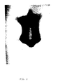
- the photoablated material is shown in figure 1 (optical microscope (44 X enlargement).
- the laser beam had a wave length of 350 nm, was emitted with an impulse time of 15 ns, the energy delivered per impulse was equal to 33 mJ, the peak power was at 2.2 MW.
- the fluency considered as energy amount irradiated per surface unit, was equal to 0.33 J/cm2.
- photoablation After application of a single irradiation impulse, at a velocity corresponding to 10 ⁇ m/impulse.
- optical microscopy scanning electron microscopy and conductivity measurements it was possible to ascertain a complete removal of the polymeric film from the examined area without any substantial alteration of the areas surrounding the photoablated area.
- a silicon plate was coated by using a solution of an acrylated perfluoropolyether monomer,prepared according to example 1 of European patent application No. 193,370, in admixture with a diacrylic monomer of example 2 of said patent, in an acrylate/diacrylate molar ratio of 2:1.
- the solution in CF2Cl-CFCl2 was at 1% by weight of total monomers and contained benzophenone, in an amount equal to 0.5% by weight referred to the monomers, as a photo-starter.
- a polymerization and cross-linking treatment by irradiation with UV-rays was carried out. A 10 ⁇ m thick coating layer was so obtained.
- the plate so coated was subjected to the photoablation process conducted as is described in the preceding example 2.
Landscapes
- Physics & Mathematics (AREA)
- General Physics & Mathematics (AREA)
- Paints Or Removers (AREA)
- Treatments Of Macromolecular Shaped Articles (AREA)
- Application Of Or Painting With Fluid Materials (AREA)
- Exposure And Positioning Against Photoresist Photosensitive Materials (AREA)
Applications Claiming Priority (2)
| Application Number | Priority Date | Filing Date | Title |
|---|---|---|---|
| IT2249387 | 1987-11-03 | ||
| IT22493/87A IT1223341B (it) | 1987-11-03 | 1987-11-03 | Procedimento di fotoablazione di film a base di polimeri a struttura pergluoroalchilpolieterea, mediante raggi laser ad eccimeri |
Publications (2)
| Publication Number | Publication Date |
|---|---|
| EP0315152A2 true EP0315152A2 (de) | 1989-05-10 |
| EP0315152A3 EP0315152A3 (de) | 1990-09-05 |
Family
ID=11197010
Family Applications (1)
| Application Number | Title | Priority Date | Filing Date |
|---|---|---|---|
| EP19880118262 Withdrawn EP0315152A3 (de) | 1987-11-03 | 1988-11-02 | Photoablativ-Verfahren für Perfluoralkylätherpolymere mittels Excimer-Laser |
Country Status (3)
| Country | Link |
|---|---|
| EP (1) | EP0315152A3 (de) |
| JP (1) | JPH0271A (de) |
| IT (1) | IT1223341B (de) |
Cited By (5)
| Publication number | Priority date | Publication date | Assignee | Title |
|---|---|---|---|---|
| US5259311A (en) * | 1992-07-15 | 1993-11-09 | Mark/Trece Inc. | Laser engraving of photopolymer printing plates |
| EP0766296A3 (de) * | 1995-09-29 | 1998-05-13 | Sony Corporation | Verfahren zur Herstellung von einem Dünnschicht-Feldeffekttransistor |
| US5798202A (en) * | 1992-05-11 | 1998-08-25 | E. I. Dupont De Nemours And Company | Laser engravable single-layer flexographic printing element |
| US5804353A (en) * | 1992-05-11 | 1998-09-08 | E. I. Dupont De Nemours And Company | Lasers engravable multilayer flexographic printing element |
| WO1999061248A1 (fr) * | 1998-05-27 | 1999-12-02 | Sagadev | Procede de fabrication d'un cliche d'impression flexographique |
Families Citing this family (3)
| Publication number | Priority date | Publication date | Assignee | Title |
|---|---|---|---|---|
| JP2725933B2 (ja) * | 1992-01-31 | 1998-03-11 | 三洋電機株式会社 | オートフォーカス装置 |
| KR100854207B1 (ko) * | 2007-04-04 | 2008-08-26 | 성공제 | 아그마틴의 망막 신경절 세포 보호 용도 |
| KR100902478B1 (ko) * | 2007-06-13 | 2009-06-11 | 성균관대학교산학협력단 | 에이전트 플랫폼. |
Family Cites Families (3)
| Publication number | Priority date | Publication date | Assignee | Title |
|---|---|---|---|---|
| FR1552904A (de) * | 1967-09-15 | 1969-01-10 | ||
| US4414059A (en) * | 1982-12-09 | 1983-11-08 | International Business Machines Corporation | Far UV patterning of resist materials |
| US4752668A (en) * | 1986-04-28 | 1988-06-21 | Rosenfield Michael G | System for laser removal of excess material from a semiconductor wafer |
-
1987
- 1987-11-03 IT IT22493/87A patent/IT1223341B/it active
-
1988
- 1988-11-02 EP EP19880118262 patent/EP0315152A3/de not_active Withdrawn
- 1988-11-02 JP JP63278491A patent/JPH0271A/ja active Pending
Cited By (7)
| Publication number | Priority date | Publication date | Assignee | Title |
|---|---|---|---|---|
| US5798202A (en) * | 1992-05-11 | 1998-08-25 | E. I. Dupont De Nemours And Company | Laser engravable single-layer flexographic printing element |
| US5804353A (en) * | 1992-05-11 | 1998-09-08 | E. I. Dupont De Nemours And Company | Lasers engravable multilayer flexographic printing element |
| US5259311A (en) * | 1992-07-15 | 1993-11-09 | Mark/Trece Inc. | Laser engraving of photopolymer printing plates |
| EP0766296A3 (de) * | 1995-09-29 | 1998-05-13 | Sony Corporation | Verfahren zur Herstellung von einem Dünnschicht-Feldeffekttransistor |
| WO1999061248A1 (fr) * | 1998-05-27 | 1999-12-02 | Sagadev | Procede de fabrication d'un cliche d'impression flexographique |
| FR2779090A1 (fr) * | 1998-05-27 | 1999-12-03 | Sagadev | Procede de fabrication d'un cliche d'impression flexographique |
| US6551762B1 (en) | 1998-05-27 | 2003-04-22 | Sagadev | Process for manufacturing a flexographic printing plate |
Also Published As
| Publication number | Publication date |
|---|---|
| JPH0271A (ja) | 1990-01-05 |
| IT8722493A0 (it) | 1987-11-03 |
| EP0315152A3 (de) | 1990-09-05 |
| IT1223341B (it) | 1990-09-19 |
Similar Documents
| Publication | Publication Date | Title |
|---|---|---|
| EP0315152A2 (de) | Photoablativ-Verfahren für Perfluoralkylätherpolymere mittels Excimer-Laser | |
| US6027849A (en) | Ablative imageable element | |
| US3779806A (en) | Electron beam sensitive polymer t-butyl methacrylate resist | |
| ATE85068T1 (de) | Loesungsmittelfreie, monomerarme bzw. -freie, polymerisierbare schmelzmasse, verfahren zu deren herstellung und verarbeitung. | |
| US6117497A (en) | Solid surface modification method and apparatus | |
| CA2075115A1 (en) | Photopolymer composition for the production of three-dimensional objects | |
| KR20240129029A (ko) | 가고정용 조성물, 가고정용 접착제 및 박형 웨이퍼의 제조 방법 | |
| JPH07328532A (ja) | 撥水性被膜 | |
| US5518865A (en) | Production of microstructure elements | |
| EP1366511B1 (de) | Herstellung eines metallischen musters | |
| GB2093048A (en) | Positive resist copolymer and method for manufacturing a pattern therewith | |
| US6689426B1 (en) | Solid surface modification method and apparatus | |
| KR950001005B1 (ko) | 광학상을 형성할 수 있는 전착가능한 포토레지스트 조성물 | |
| Popall et al. | Inorganic-organic composites (ORMOCERs) as structured layers for microelectronics | |
| US3674591A (en) | Surface deformation imaging process | |
| Van Dyke et al. | Modification of fluoropolymer surfaces with electronically conductive polymers | |
| EP0535750B1 (de) | Verfahren zur Pfropfung von hydrophilen Monomeren enthaltenden Doppelbindungen auf geformten Körpern mit Polymeroberflächen | |
| JPH08139067A (ja) | 半導体ウエハに付着した異物の除去用粘着テ―プと除去方法 | |
| EP0253237A2 (de) | Verfahren zum Fotoätzen von polymerartigen Oberflächenbeschichtungen | |
| JP3303238B2 (ja) | グラビア印刷媒体及びグラビア印刷装置に使用される媒体を製造する方法 | |
| JPS6332810B2 (de) | ||
| EP1280654A1 (de) | Verfahren zum aufbringen einer polymermaterial enthaltenden schicht | |
| JP2549425B2 (ja) | 活性エネルギー線硬化型樹脂組成物 | |
| JP3192680B2 (ja) | 基材を被覆する方法 | |
| JP3191889B2 (ja) | 液晶基板の帯電防止方法 |
Legal Events
| Date | Code | Title | Description |
|---|---|---|---|
| PUAI | Public reference made under article 153(3) epc to a published international application that has entered the european phase |
Free format text: ORIGINAL CODE: 0009012 |
|
| AK | Designated contracting states |
Kind code of ref document: A2 Designated state(s): BE DE FR GB NL SE |
|
| PUAL | Search report despatched |
Free format text: ORIGINAL CODE: 0009013 |
|
| AK | Designated contracting states |
Kind code of ref document: A3 Designated state(s): BE DE FR GB NL SE |
|
| 17P | Request for examination filed |
Effective date: 19901206 |
|
| STAA | Information on the status of an ep patent application or granted ep patent |
Free format text: STATUS: THE APPLICATION IS DEEMED TO BE WITHDRAWN |
|
| 18D | Application deemed to be withdrawn |
Effective date: 19930602 |