EP0316774A2 - Appareil à cristaux à cristaux liquides - Google Patents
Appareil à cristaux à cristaux liquides Download PDFInfo
- Publication number
- EP0316774A2 EP0316774A2 EP88118766A EP88118766A EP0316774A2 EP 0316774 A2 EP0316774 A2 EP 0316774A2 EP 88118766 A EP88118766 A EP 88118766A EP 88118766 A EP88118766 A EP 88118766A EP 0316774 A2 EP0316774 A2 EP 0316774A2
- Authority
- EP
- European Patent Office
- Prior art keywords
- scanning
- electrodes
- voltage
- selection signal
- liquid crystal
- Prior art date
- Legal status (The legal status is an assumption and is not a legal conclusion. Google has not performed a legal analysis and makes no representation as to the accuracy of the status listed.)
- Granted
Links
Images


Classifications
-
- G—PHYSICS
- G02—OPTICS
- G02F—OPTICAL DEVICES OR ARRANGEMENTS FOR THE CONTROL OF LIGHT BY MODIFICATION OF THE OPTICAL PROPERTIES OF THE MEDIA OF THE ELEMENTS INVOLVED THEREIN; NON-LINEAR OPTICS; FREQUENCY-CHANGING OF LIGHT; OPTICAL LOGIC ELEMENTS; OPTICAL ANALOGUE/DIGITAL CONVERTERS
- G02F1/00—Devices or arrangements for the control of the intensity, colour, phase, polarisation or direction of light arriving from an independent light source, e.g. switching, gating or modulating; Non-linear optics
- G02F1/01—Devices or arrangements for the control of the intensity, colour, phase, polarisation or direction of light arriving from an independent light source, e.g. switching, gating or modulating; Non-linear optics for the control of the intensity, phase, polarisation or colour
- G02F1/13—Devices or arrangements for the control of the intensity, colour, phase, polarisation or direction of light arriving from an independent light source, e.g. switching, gating or modulating; Non-linear optics for the control of the intensity, phase, polarisation or colour based on liquid crystals, e.g. single liquid crystal display cells
- G02F1/133—Constructional arrangements; Operation of liquid crystal cells; Circuit arrangements
- G02F1/1333—Constructional arrangements; Manufacturing methods
- G02F1/1343—Electrodes
- G02F1/134309—Electrodes characterised by their geometrical arrangement
- G02F1/134336—Matrix
-
- G—PHYSICS
- G09—EDUCATION; CRYPTOGRAPHY; DISPLAY; ADVERTISING; SEALS
- G09G—ARRANGEMENTS OR CIRCUITS FOR CONTROL OF INDICATING DEVICES USING STATIC MEANS TO PRESENT VARIABLE INFORMATION
- G09G3/00—Control arrangements or circuits, of interest only in connection with visual indicators other than cathode-ray tubes
- G09G3/20—Control arrangements or circuits, of interest only in connection with visual indicators other than cathode-ray tubes for presentation of an assembly of a number of characters, e.g. a page, by composing the assembly by combination of individual elements arranged in a matrix no fixed position being assigned to or needed to be assigned to the individual characters or partial characters
- G09G3/34—Control arrangements or circuits, of interest only in connection with visual indicators other than cathode-ray tubes for presentation of an assembly of a number of characters, e.g. a page, by composing the assembly by combination of individual elements arranged in a matrix no fixed position being assigned to or needed to be assigned to the individual characters or partial characters by control of light from an independent source
- G09G3/36—Control arrangements or circuits, of interest only in connection with visual indicators other than cathode-ray tubes for presentation of an assembly of a number of characters, e.g. a page, by composing the assembly by combination of individual elements arranged in a matrix no fixed position being assigned to or needed to be assigned to the individual characters or partial characters by control of light from an independent source using liquid crystals
- G09G3/3607—Control arrangements or circuits, of interest only in connection with visual indicators other than cathode-ray tubes for presentation of an assembly of a number of characters, e.g. a page, by composing the assembly by combination of individual elements arranged in a matrix no fixed position being assigned to or needed to be assigned to the individual characters or partial characters by control of light from an independent source using liquid crystals for displaying colours or for displaying grey scales with a specific pixel layout, e.g. using sub-pixels
-
- G—PHYSICS
- G09—EDUCATION; CRYPTOGRAPHY; DISPLAY; ADVERTISING; SEALS
- G09G—ARRANGEMENTS OR CIRCUITS FOR CONTROL OF INDICATING DEVICES USING STATIC MEANS TO PRESENT VARIABLE INFORMATION
- G09G3/00—Control arrangements or circuits, of interest only in connection with visual indicators other than cathode-ray tubes
- G09G3/20—Control arrangements or circuits, of interest only in connection with visual indicators other than cathode-ray tubes for presentation of an assembly of a number of characters, e.g. a page, by composing the assembly by combination of individual elements arranged in a matrix no fixed position being assigned to or needed to be assigned to the individual characters or partial characters
- G09G3/34—Control arrangements or circuits, of interest only in connection with visual indicators other than cathode-ray tubes for presentation of an assembly of a number of characters, e.g. a page, by composing the assembly by combination of individual elements arranged in a matrix no fixed position being assigned to or needed to be assigned to the individual characters or partial characters by control of light from an independent source
- G09G3/36—Control arrangements or circuits, of interest only in connection with visual indicators other than cathode-ray tubes for presentation of an assembly of a number of characters, e.g. a page, by composing the assembly by combination of individual elements arranged in a matrix no fixed position being assigned to or needed to be assigned to the individual characters or partial characters by control of light from an independent source using liquid crystals
- G09G3/3611—Control of matrices with row and column drivers
- G09G3/3622—Control of matrices with row and column drivers using a passive matrix
- G09G3/3629—Control of matrices with row and column drivers using a passive matrix using liquid crystals having memory effects, e.g. ferroelectric liquid crystals
- G09G3/364—Control of matrices with row and column drivers using a passive matrix using liquid crystals having memory effects, e.g. ferroelectric liquid crystals with use of subpixels
-
- G—PHYSICS
- G02—OPTICS
- G02F—OPTICAL DEVICES OR ARRANGEMENTS FOR THE CONTROL OF LIGHT BY MODIFICATION OF THE OPTICAL PROPERTIES OF THE MEDIA OF THE ELEMENTS INVOLVED THEREIN; NON-LINEAR OPTICS; FREQUENCY-CHANGING OF LIGHT; OPTICAL LOGIC ELEMENTS; OPTICAL ANALOGUE/DIGITAL CONVERTERS
- G02F1/00—Devices or arrangements for the control of the intensity, colour, phase, polarisation or direction of light arriving from an independent light source, e.g. switching, gating or modulating; Non-linear optics
- G02F1/01—Devices or arrangements for the control of the intensity, colour, phase, polarisation or direction of light arriving from an independent light source, e.g. switching, gating or modulating; Non-linear optics for the control of the intensity, phase, polarisation or colour
- G02F1/13—Devices or arrangements for the control of the intensity, colour, phase, polarisation or direction of light arriving from an independent light source, e.g. switching, gating or modulating; Non-linear optics for the control of the intensity, phase, polarisation or colour based on liquid crystals, e.g. single liquid crystal display cells
- G02F1/133—Constructional arrangements; Operation of liquid crystal cells; Circuit arrangements
- G02F1/1333—Constructional arrangements; Manufacturing methods
- G02F1/1343—Electrodes
- G02F1/134309—Electrodes characterised by their geometrical arrangement
- G02F1/134345—Subdivided pixels, e.g. for grey scale or redundancy
-
- G—PHYSICS
- G09—EDUCATION; CRYPTOGRAPHY; DISPLAY; ADVERTISING; SEALS
- G09G—ARRANGEMENTS OR CIRCUITS FOR CONTROL OF INDICATING DEVICES USING STATIC MEANS TO PRESENT VARIABLE INFORMATION
- G09G2310/00—Command of the display device
- G09G2310/02—Addressing, scanning or driving the display screen or processing steps related thereto
- G09G2310/0224—Details of interlacing
- G09G2310/0227—Details of interlacing related to multiple interlacing, i.e. involving more fields than just one odd field and one even field
-
- G—PHYSICS
- G09—EDUCATION; CRYPTOGRAPHY; DISPLAY; ADVERTISING; SEALS
- G09G—ARRANGEMENTS OR CIRCUITS FOR CONTROL OF INDICATING DEVICES USING STATIC MEANS TO PRESENT VARIABLE INFORMATION
- G09G2310/00—Command of the display device
- G09G2310/06—Details of flat display driving waveforms
-
- G—PHYSICS
- G09—EDUCATION; CRYPTOGRAPHY; DISPLAY; ADVERTISING; SEALS
- G09G—ARRANGEMENTS OR CIRCUITS FOR CONTROL OF INDICATING DEVICES USING STATIC MEANS TO PRESENT VARIABLE INFORMATION
- G09G2310/00—Command of the display device
- G09G2310/06—Details of flat display driving waveforms
- G09G2310/061—Details of flat display driving waveforms for resetting or blanking
-
- G—PHYSICS
- G09—EDUCATION; CRYPTOGRAPHY; DISPLAY; ADVERTISING; SEALS
- G09G—ARRANGEMENTS OR CIRCUITS FOR CONTROL OF INDICATING DEVICES USING STATIC MEANS TO PRESENT VARIABLE INFORMATION
- G09G2310/00—Command of the display device
- G09G2310/06—Details of flat display driving waveforms
- G09G2310/065—Waveforms comprising zero voltage phase or pause
-
- G—PHYSICS
- G09—EDUCATION; CRYPTOGRAPHY; DISPLAY; ADVERTISING; SEALS
- G09G—ARRANGEMENTS OR CIRCUITS FOR CONTROL OF INDICATING DEVICES USING STATIC MEANS TO PRESENT VARIABLE INFORMATION
- G09G2320/00—Control of display operating conditions
- G09G2320/02—Improving the quality of display appearance
- G09G2320/0247—Flicker reduction other than flicker reduction circuits used for single beam cathode-ray tubes
-
- G—PHYSICS
- G09—EDUCATION; CRYPTOGRAPHY; DISPLAY; ADVERTISING; SEALS
- G09G—ARRANGEMENTS OR CIRCUITS FOR CONTROL OF INDICATING DEVICES USING STATIC MEANS TO PRESENT VARIABLE INFORMATION
- G09G3/00—Control arrangements or circuits, of interest only in connection with visual indicators other than cathode-ray tubes
- G09G3/20—Control arrangements or circuits, of interest only in connection with visual indicators other than cathode-ray tubes for presentation of an assembly of a number of characters, e.g. a page, by composing the assembly by combination of individual elements arranged in a matrix no fixed position being assigned to or needed to be assigned to the individual characters or partial characters
- G09G3/2007—Display of intermediate tones
- G09G3/2074—Display of intermediate tones using sub-pixels
Definitions
- the present invention relates to a liquid crystal apparatus, such as a display panel or a shutter-array printer, using a ferroelectric liquid crystal.
- liquid crystal display devices which comprises a group of scanning electrodes and a group of signal or data electrodes arranged in a matrix, and a liquid crystal compound is filled between the electrode groups to form a large number of pixels thereby to display images or information.
- These display devices are driven by a multiplexing driving method wherein an address signal is selectively applied sequentially and periodically to the group of scanning electrodes, and prescribed data signals are parallely and selectively applied to the group of data electrodes in synchronism with the address signals.
- TN (twisted nematic)-type liquid crystals have been used as described in "Voltage-Dependent Optical Activity of a Twisted Nematic Liquid Crystal" by M. Schadt and W. Helfrich, Applied Physics Letters, Vol. 18, No. 4, pp. 127 - 128.
- a ferroelectric liquid crystal (hereinafter sometimes abbreviated as "FLC") showing chiral smectic C phase (SmC*) or H phase (SmH*) is generally used.
- FLC ferroelectric liquid crystal
- the ferroelectric liquid crystal assumes either a first optically stable state or a second optically stable state in response to an electric field applied thereto and retains the resultant state in the absence of an electric field, thus showing a bistability.
- the ferroelectric liquid crystal quickly responds to a change in electric field, and thus the ferroelectric liquid crystal device is expected to be widely used in the field of a high-speed and memory-type display apparatus, etc.
- EP-A 149899 discloses a multiplex driving method comprising applying a scanning selection signal of an AC voltage the polarity of which is reversed (or the signal phase of which is reversed) for each frame to selectively write a "white” state (in combination with cross nicol polarizers arranged to provide a "bright” state at this time) in a frame and then selectively write a "black” state (in combination with the cross nicol polarizers arranged to provide a "dark” state at this time).
- those driving methods as disclosed by U.S. Patents Nos. 4548476 and 4655561 have been known.
- the white background causes flickering. Occurrence of a similar flickering is observable also on a display of white characters on the black background opposite to the above case.
- an ordinary frame frequency is 30 Hz
- the above half-selection voltage is applied at a frequency of 15 Hz which is a 1/2 frame frequency, so that it is sensed by an observer as a flickering to remarkably degrade the display quality.
- An object of the present invention is to provide a ferroelectric liquid crystal apparatus wherein occurrence of flickering caused by a low frame frequency scanning drive, e.g., 15 Hz or below, is suppressed.
- Another object of the present invention is to provide a ferroelectric liquid crystal apparatus for realizing a gradational display free from flickering.
- a further object of the present invention is to provide a ferroelectric liquid crystal apparatus with an improved display quality and a broad driving margin.
- a liquid crystal apparatus comprising:
- a screen for a picture display is defined by the electrode matrix.
- picture scanning refers to scanning of all the scanning electrodes constituting or covering all or a prescribed part of the screen for giving a desired picture.
- a liquid crystal apparatus comprising:
- a liquid crystal apparatus comprising:
- FLC ferroelectric liquid crystal
- Figure 1 is a schematic plan view of a matrix electrode structure of an FLC device according to an embodiment of the present invention and Figure 2 is a sectional view taken along the line A-A′ in Figure 1.
- the FLC device comprises upper electrodes 11A (A1, A2, A3, ...) and 11B (B1, B2, B3, B4, ...) constituting data electrodes, and lower electrodes 12 constituting scanning electrodes C (C0, C1, C2, C3, ).
- These data electrodes 11A, 11B and scanning electrodes 12 are formed on glass substrates 13 and 14, respectively, and mutually arranged so as to form a matrix with an FLC material 15 disposed therebetween.
- one pixel is constituted by a region E surrounded by a dashed line, i.e., a region where a scanning electrode C (C2 is shown as an example) and two data electrodes A (A2) and B (B2) (electrode width: A > B).
- each data electrode A is composed to have a wider electrode width then an accompanying data electrode B.
- the scanning electrodes C and the data electrodes A, B are respectively connected to a power supply (not shown) through switches SW (or equivalents thereof).
- the switches SW are also connected to a controller unit (not shown) for controlling the ON/OFF of the switches.
- a gray scale display in the pixel E may be effected under the control by means of the controller circuit as follows.
- a white display state (“W") is given by applying a "W” signal to the data electrodes A2 and B2 respectively;
- a display state of "Gray 1” is given by applying a "W" signal to A2 and a black (“B") signal to B2;
- a display state of "Gray 2” is given by applying a "B" signal to A2 and a “W” signal to B2;
- a black display state (“B") is given by applying a "B” signal to A2 and B2 respectively.
- Figure 3 shows the resultant states W, Gray 1, Gray 2 and B constituting a gray scale.
- a pixel E is composed of a plural number ( n ) of intersections of electrodes having intersection areas giving a geometric series of ratios such as 1:2:4:8: ...:2 n-1 (the minimum intersection area is taken as 1 (unit)).
- a scanning electrode is divided into two electrode stripes having widths C and D and combined with the data electrodes A and B (A ⁇ B)
- 16 gradation levels can be provided when C ⁇ D.
- the polarizers 16A and 16B are disposed to have their polarization axes intersecting each other, and the intersecting polarization axes may preferably be disposed to provide a dark state in an erasure phase which will be explained hereinafter.
- the electrode matrix shown in Figure 1 may be driven according to a driving method as will be described hereinbelow.
- a scanning selection signal is sequentially applied to the scanning electrodes two or more scanning electrodes apart or very third or more electrode so as to effectively suppress the occurrence of flickering in scanning drive at a low frame frequency.
- a scanning selection signal is sequentially applied to the scanning electrodes two or more scanning electrodes apart or very third or more electrode so as to effectively suppress the occurrence of flickering in scanning drive at a low frame frequency.
- the occurrence of flickering can be suppressed in scanning drive at an even lower frequency.
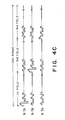
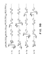
- Figures 4A - 4E show driving waveforms used in the present invention. More specifically, Figure 4A shows a scanning selection signal S S , a scanning non-selection signal S N , a white data signal I W and a black data signal I B .
- a pixel on a selected scanning electrode to which a scanning selection signal is applied is supplied with a white data signal I W through a data electrode, the pixel is erased into a dark state (black) in phase T1 as a result of application of a voltage V2 at phase t1 and a voltage V2 + V3 at phase t2, and is then written in ai bright state (white) at a subsequently phase t3 by application of a voltage -(V1 + V3).
- the above-mentioned scanning selection signal is applied to the scanning electrodes according to interlaced scanning of two or more scanning electrodes apart.
- Figure 4B shows an example where the scanning selection signal is applied two scanning electrodes apart, i.e., every third scanning electrode.
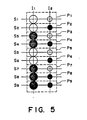
- Figure 4C shows an example set of driving waveforms whereby a display state shown in Figure 5 is obtained.
- Figure 5 denotes a black written state and denotes a white written state.
- each intersection of scanning electrodes S1 - S9 and a data electrodes I1 is set to have an area (pixel area) which is twice that of each intersection of the scanning electrodes S1 - S9 and a data electrode I2 to form pixels P1 - 9.
- the pixels P1 - P4 display four gradation levels due to differences in proportions of black and white states.
- scanning electrodes have been selected by interlaced scanning of two scanning electrodes apart.
- selection or interlaced scanning of scanning electrodes can be effected three, four, ... or N electrodes apart.
- one frame scanning may include N+1 fields of scanning.
- an interlaced scanning system of 8 or more lines apart may be effective for suppressing the flickering.
- the order of scanning electrodes to which the scanning selection signal is applied sequentially does not correspond to the order of field.
- the scanning selection signal is applied to scanning electrodes which are not adjacent to each other.
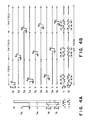
- Figure 4E shows another embodiment of the above scheme (interlaced scanning of 3 lines apart).
- the driving scheme adopted is the embodiments of Figs. 4D and 4E is more effective in suppressing the occurrence of flickering than in the scanning signal application scheme shown in Figure 4B.
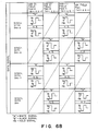
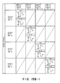
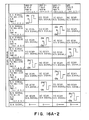
- Figures 6 - 14 show interlaced scanning schemes wherein a scanning selection signal is selectively applied to every other scanning electrode.
- one field means one vertical scanning operation or period).
- the scanning selection signal S 4n-3 has voltage polarities (with respect to the voltage level of a scanning non-selection signal) which are opposite to each other in the corresponding phases of the (4M-3)th field F 4M-3 and (4M-1)th field F 4M-1 , while the scanning selection signal S 4n-3 is so composed as to effect no scanning i.e. so as to be a scanning non-selection signal, in the (4M-2)th field F 4M-2 or 4Mth field F 4M .
- the scanning selection signal S 4n-1 is similar, but the scanning selection signal S 4n-3 and S 4n-1 applied in one field period have different voltage waveforms and have mutually opposite voltage polarities in the corresponding phases.
- the scanning selection signal S 4n-2 has voltage polarities (with respect to the voltage level of the scanning non-selection signal) which are mutually opposite in the corresponding phases of the (4M-2)th field F 4M-2 and 4Mth field F 4M and effects no scan in the (4M-3)th field F 4M-3 or (4M-1)th field F 4M-1 .
- the scanning selection signal S 4n is similar, but the scanning selection signals S 4n-2 and S 4n applied in one field period have different voltage waveforms and have mutually opposite voltage polarities in the corresponding phases.
- a third phase is disposed for providing a pause to the whole picture (e.g., by applying a voltage of 0 simultaneously to all the pixels constituting the picture), and for this purpose, the scanning selection signals are set to have a voltage of zero (the same voltage level as the scanning non-selection signal).
- data signals applied to data electrodes in the (4M-3)th field F 4M-3 comprise a white signal (one for providing a voltage 3V0 exceeding a threshold voltage of the FLC at the second phase in combination with the scanning selection signal S 4n-3 to form a white pixel) and a hold signal (one for applying to a pixel a voltage ⁇ V0 below the threshold voltage of the FLC in combination with the scanning selection signal S 4n-3 ) which are selectively applied in synchronism with the scanning selection signal S 4n-3 ; and a black signal (for providing a voltage -3V0 exceeding a threshold voltage of the FLC at the second phase in combination with the scanning selection signal S 4n-1 to form a black pixel) and a hold signal (for applying to a pixel a voltage ⁇ V0 below the threshold voltage of the ferroelectric liquid crystal in combination with the scanning selection signal S 4n-1 ) which are selectively applied in synchronism with the scanning selection signal S 4n-1 .
- the (4n) a white signal
- data signals applied to the data electrodes comprise the above-mentioned white signal and hold signal which are selectively applied in synchronism with the scanning selection signal S 4n-2 ; and the above-mentioned black signal and hold signal which are selectively applied in synchronism with the scanning selection signal S 4n .
- the (4n-3)th and (4n-1)th scanning electrodes are supplied with a scanning non-selection signal so that the data signals are applied as they are to the pixels on these scanning electrodes.
- data signals applied to the data electrodes comprise the above-mentioned white signal and hold signal which are selectively applied in synchronism with the scanning selection signal S 4n-3 ; and the above-mentioned white signal and hold signal which are selectively applied in synchronism with the scanning selection signal S 4n-1 .
- the (4n-2)th and (4n)th scanning electrodes are supplied with a scanning non-selection signal so that the data signals are applied as they are to the pixels on these scanning electrodes.
- data signals applied to the data electrodes comprise the above-mentioned black signal and hold signal which are selectively applied in synchronism with the scanning selection signal S 4n-2 ; and the above-mentioned white signal and hold signal which are selectively applied in synchronism with the scanning selection signal S 4n .
- the (4n-3)th and (4n-1)th scanning electrodes are supplied with a scanning non-selection signal so that the data signals are applied as they are to the pixels on these scanning electrodes.
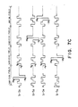
- Figures 7A, 7B and 7C are time charts showing successions of driving waveforms shown in Figures 6A and 6B used for writing to form a display state shown in Figure 12.
- Figure 12 denotes a pixel written in white and denotes a pixel written in black.
- I1 - S1 is shown a time-serial voltage waveform applied to the intersection of a scanning electrode S1 and a data electrode I1.
- I2 - S1 is shown a time-serial waveform applied to the intersection of the scanning electrode S1 and a data electrode I2.
- I1 - S2 is shown a time-serial voltage waveform applied to the intersection of a scanning electrode S2 and the data electrode I1; and at I2 - S2 is shown a time-serial voltage waveform applied to the intersection of the scanning electrode S2 and the data electrode I2.
- a gradational display may be effected by applying the embodiment of Figures 6A and 6B as well as one shown in Figures 8A and 8B explained hereinbelow to an electrode matrix as shown in Figure 1.
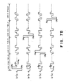
- FIGs 8A and 8B show another set of driving waveforms used in the present invention.
- each of the scanning selection signals S 4n-3 and S 4n-1 comprises two voltage waveforms which are of mutually opposite polarities with respect to the voltage level of a scanning non-selection signal, and each of the scanning selection signals comprises a former pulse and a latter pulse, the former having a duration twice that of the latter.
- each data signal is characterized by having a voltage of zero at the first phase and alternating voltages at the first and third phases which are of mutually opposite polarities with respect to the scanning non-selection signal voltage.
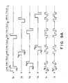
- Figures 9A - 9C are time charts showing successions of driving waveforms shown in Figures 8A and 8B used for writing to form the display state shown in Figure 12.
- Figures 10 (10A and 10B) and 11 (11A and 11B) respectively show another preferred set of driving waveforms used in the present invention.
- the scanning selection signals and the data signals are designed to have two voltage levels so that designing of a driving circuit therefor is simplified.
- the amplitude of a scanning selection signal is set to 2
- the amplitude of a scanning selection signal
- the above-mentioned voltage V0 may be set to satisfy the following relationships: V0 ⁇ V th1 ⁇ 3V0, and -3V0 ⁇ -V th2 ⁇ -V0.
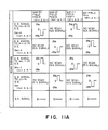
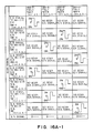
- Table 1 shows a time relation of a white selection voltage S W for forming white selection pixels and a half-selection voltage H applied as that time in fields F1, F2, F3, F4 , ...
- Table 2 shows another time relation for forming white selection pixels.
- a white selection voltage S W is applied to pixels (white selection pixels) on (4N-3)th scanning lines S1, S5, ...
- a half-selection voltage is applied to pixels (white selection pixels) on (4N-1)th scanning lines S3, S7, ...
- the pixels on (4N-2)th and (4N)th scanning electrodes S2, S4, S6, S8, ... are not scanned.
- pixels (white selection pixels) on all the scanning lines are supplied with a white selection voltage in the odd-numbered fields F1, F3 ...
- pixels (white selection pixels) on all the scanning lines are supplied with a half-selection voltage in the even-numbered fields.
- the flickering occurs at a frequency of 60 Hz.
- the number of pixels supplied with a half-selection voltage is reduced to 1/4 of that according to the method of Table 2, whereby the flickering is effectively prevented by that much.
- pixels (white selection pixels) on the odd-numbered scanning lines S1, S3, ... are supplied with a white selection voltage and pixels (white selection pixels) on the even-numbered scanning lines S2, S4, ... are supplied with a half-selection voltage so that flickering occurs at the field frequency (equal to the frame frequency because all the scanning lines are scanned in one vertical scanning according to Table 3).
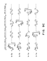
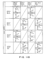
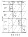
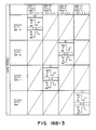
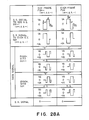
- FIGS 13A and 13B show still another set of driving waveforms used in the present invention.
- the scanning selection signal S 4n-3 applied to the (4n-3)th scanning electrode (or the scanning selection signal S 4n-1 applied to the (4n-1)th scanning electrode) in the (4M-3)th field F 4M-3 and the scanning selection signal S 4n-2 applied to the (4n-1)th scanning electrode (or the scanning selection signal S 4n applied to the 4n-th scanning electrode) in the (4M-2)th field F 4M-2 are the same.
- S 4n-3 (or S 4n-1 ) in F 4M-3 and S 4n-2 (or S 4n ) in F 4M-2 have mutually different voltage waveforms and have mutually opposite voltage polarities in the corresponding phases.
- Table 4 shows a time relation of a white selection voltage S W for forming white selection pixels and a half-selection voltage H applied at that time in fields F1, F2, F3, F4 ... according to the driving embodiment shown in Figure 13.
- the driving embodiment of Figure 13 is effective for preventing flickering similarly as the embodiment shown in Figure 6 except that the time relation between the application of a white-selection voltage S W and that of a half-section voltage in fields F1, F2, F3, F4, ... are different from those shown in Figure 6.
- the present invention is not limited to a particular time relation according to which a selection voltage and a half-selection voltage are applied in each field.
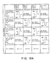
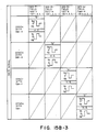
- Figures 14A and 14B show a further set of driving waveforms used in the present invention.
- the time for applying a selection voltage is shifted to a next (or preceding) scanning line for each field as is understood from Table 1 (or Table 4). More specifically, if it is assumed that a scanning line Sn is selected in an n-th field, a scanning line S n+1 (or S n-1 ) is selected in an (n+1)th field and a scanning line S n+2 (or S n-2 ) is selected in an (n+2)th field. In this way, the time for applying a selection voltage is shifted sequentially for each field.
- the contrast occurs at the time of applying a selection voltage to a scanning line and is sequentially moved on a screen like a line flow to result in a remarkable degradation in display quality.
- Table 5 below shows a time relation for application of a white selection voltage S w and a half-selection voltage H at that time applied to pixels in fields F1, F2, F3, F4, ... by using the driving embodiment shown in Figure 14 (14A and 14B).
- the driving embodiment shown in Figures 14A and 14B has been designed to remove a problem caused accompanying a time relation of applying selection voltages.
- the sequential movement of a point of applying a selection voltage in one direction is prevented to the utmost while avoiding degradation in display quality.
- the present invention also provides a solution to a problem caused by a time relation of applying a selection voltage and a half-selection voltage in each field.
- Figures 15A and 15B show still another driving embodiment of the present invention.
- the number of scanning lines scanned in one vertical scanning period is 1/2 of the total scanning lines and all the scanning lines are scanned in two times of vertical scanning.
- every fourth scanning line is scanned in one vertical scanning period, and a scanning line next to the one scanned in the previous vertical scanning period is scanned in the next vertical scanning period. Accordingly, the number of scanning lines scanned in one vertical scanning period is 1/4 of the total scanning lines, so that all the scanning lines are scanned in four times of vertical scanning.
- Table 6 below shows a time relation for application of a white selection voltage S W and a half-selection voltage H applied to pixels in fields F1, F2, F3, F4, ... by using the driving embodiment shown in Figure 15 (15A and 15B).
- pixels (white selection pixels) on (8M-7)th scanning lines S 1 S9, ... are supplied with a white selection voltage; pixels (white selection pixels) on (8M-3)th scanning lines S5, S13, ... are supplied with a half-selection voltage; and pixels on (8N-6)th, (8N-5)th, (8N-4)th, (8N-2)th, (8N-1)th and (8N)th scanning lines S2, S3, S4, S6, S7, S8 ... are not scanned.
- all the scanning lines are not scanned in one time of vertical scanning but in several times of vertical scanning so as to prevent flickering.
- the number of vertical scanning required for vertical scanning is not particularly limited as far as it is at least two times.
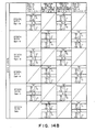
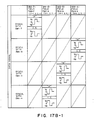
- FIGS 16A and 16B show still another driving embodiment of the present invention.
- (8N-7)th and (8N-3)th scanning lines are scanned in an (8M-7)th field
- (8N-6)th and (8N-2)th scanning lines are scanned in the subsequent (8M-6)th field.
- a scanning line next to the one scanned in a previous field is scanned in the next field
- a further next scanning line is scanned in the subsequent field, and so on.
- the time or point for applying a selection voltage is shifted sequentially for each field.
- the contrast occurs at the time of applying a selection voltage to a scanning line and is sequentially moved on a screen like a line flow to result in a remarkable degradation in display quality.
- Table 7 shows a time relation for application of a white selection voltage S W and a half-selection voltage H at that time applied to pixels in fields F1, F2, F3, F4, ... by using the driving embodiment shown in Figure 16 (16A and 16B).
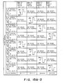
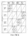
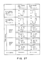
- Figure 17 (17A and 17B) shows still another preferred driving embodiment of the present invention.
- a scanning selection signal is applied to every fourth scanning electrode in a field, and the scanning electrodes selected in two consecutive fields are not adjacent to each other.
- all the scanning lines are scanned in at least two times of vertical scanning to prevent the occurrence of flickering, and the order of scanning scanning lines is not limited.
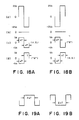
- Figure 18A shows driving waveforms used in an odd-numbered frame
- Figure 18B shows driving waveforms used in an even-numbered frame
- a scanning selection signal at (a) is shown a scanning selection signal
- at (b) is shown a scanning non-selection signal
- at (c) and (d) are shown data signals comprising two bipolar voltages of mutually anti-phases.
- the data signal at (c) functions as a hold signal (H.S.)
- the data signal at (d) functions as a white (or black) writing signal
- the data signal at (c) functions as a black (or white) writing signal
- the data signal at (d) functions as a hold signal.
- Figure 19A shows a driving waveform applied to a certain noted pixel (formed at an intersection of a scanning electrode and a data electrode) the time of non-selection when supplied with "white (or black)" - “hold” signals
- Figure 19B shows a driving waveform applied to such a pixel when supplied with “black (or white” - “hold” signals.
- ⁇ T unit pulse duration
- a certain noted pixel at the time of non-selection is supplied with a pulse component of 2 ⁇ T duration.
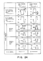
- a display of a white image on a black background was formed while applying a scanning selection signals periodically and repeatedly to the scanning electrodes.
- a display obtained at that time is schematically shown in Figure 20.
- a display panel 201 has a scanning electrode side 202 and a data electrode side 203, on the panel 201 are formed a black background, white image portions 205a and pale black or gray background portions 205b
- gray or pale black background portions were formed at regions expected to form a part of the black background along the data electrodes providing the white image portions. Such a display state degrades the display quality and is not desirable.
- a driving waveform shown in Figure 21A was applied to an intersection P1 of a scanning electrode S n and a data electrode I shown in Figure 20.
- the data electrode I was supplied with data signals of B ⁇ B ⁇ B ⁇ B ⁇ W ⁇ W (B: black, W: white) in synchronism with the scanning signals applied to the scanning electrodes S n , S n+1 , S n+2 , S n+3 , S n+4 , S n+5 and S n+6 .
- Figure 21B shows an optical response obtained at that time measured by a photomultiplier.
- the intersection P1 was supplied with a pulse with a duration of 2 ⁇ T at the time of switching of data signals from B ⁇ W, which caused an optical fluctuation 211 as shown in Figure 21B. Accordingly, such an optical "fluctuation" was cased based on occurrence of pale black background portions. The above phenomenon was remarkably observed particularly in a refresh drive scheme wherein a scanning selection signal was periodically applied.
- a liquid crystal apparatus comprising a) a liquid crystal device comprising an electrode matrix composed of scanning electrodes an data electrodes, and a ferroelectric liquid crystal; and b) a driving means including: a first means for selecting at least one scanning electrode and applying to the selected at least one scanning electrode a scanning selection signal which comprises a pulse of one polarity and a pulse of the other polarity with respect to the voltage level of a non-selected scanning electrode, said pulses of one and the other polarities having mutually different pulse durations, and a second means for applying data signals to the data electrode, each data signal comprising a pulse of one polarity and a pulse of the other polarity with respect to the voltage level of a non-selected scanning electrode, the pulses of one and the other polarities having mutually different pulse durations, a pulse having the largest pulse duration of the pulses being synchronized with the pulse at the last phase of the scanning selection signal.
- Figures 22 - 28 show driving waveforms used in the present invention for suppressing the above- mentioned "fluctuation”.
- the signal S 2n-1 comprises a voltage -V S (with respect to the voltage of a scanning non-selection signal) at a first phase t1, a voltage V S at a second phase t2 and a voltage 0 at a final phase t3.
- the pulse duration of the voltage V S at phase t2 is set to be at least twice, preferably twice, the pulse duration of the voltage -V S at phase t1.
- the signal S 2n comprises voltages of opposite polarities to those of the scanning selection signal S 2n-1 at phases t1 and t2, respectively.
- an scanning non-selection signal S 2n-1 applied to an odd-number scanning electrode has the same waveform as the scanning selection signal S 2n applied in the odd-numbered frame F 2M-1
- an scanning non-selection signal S 2n applied to an even-numbered scanning electrode has the same waveform as the scanning selection signal S 2n-1 applied in the odd-numbered frame F 2M-1 .
- the data electrodes are selectively supplied with a white signal, a black signal or a hold signal.
- the white signal comprises a voltage V D synchronized at phase t1, a voltage -V D synchronized at phase t2 and a voltage V D synchronized at phase t3.
- the pulse duration of the voltage -V D at phase t2 of the white signal is likewise set to be at least twice, preferably twice, the pulse duration of the voltage V D at the first phase t1.
- the black signal comprises voltages of opposite polarities to those of the white signal at phases t1, t2 and t3, respectively.
- a hold signal synchronized with the scanning selection signal S 2n-1 is set to have the same waveform as the above mentioned black signal, and a hold signal synchronized with the scanning selection signal S 2n is set to have the same waveform as the above-mentioned white signal.
- a hold signal synchronized with the scanning selection signal S 2n-1 is set to have the same waveform as the white signal, and a hold signal synchronized with the scanning selection signal S 2n is set to have the same waveform as the black signal.
- the maximum duration (Tb) of a single polarity voltage applied to a pixel at the time of non-selection is ⁇ t so that it has become possible to solve the problem caused in the prior art embodiment where the maximum duration has been 2 ⁇ t.
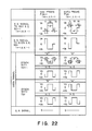
- FIG 23 shows a driving embodiment which is a modification of the one shown in Figure 22.
- scanning selection signals S 2n-1 and S 2n are respectively set to have voltages of V S (or -V S ) and -V S (or V S ) of mutually opposite polarities at a first phase t1, and a second phase t2 and are both set to have a voltage of zero at a last phase t3.
- the signals are set to have a pulse duration of ⁇ t at phase t2 and a pulse duration of 3/2 ⁇ t at phase t1, and the voltage 0 is set to have a duration of ⁇ t/2.
- a white signal, a black signal and a hold signal comprise voltages V D and -V D of mutually opposite polarities applied in synchronism with phase t1 of the scanning selection signals S 2n-1 and S 2n .
- a first applied voltage V D or -V D is set to have a pulse duration ⁇ t/2 and a next applied voltage -V D or V D is set to have a duration ⁇ t.
- the white signal, black signal and hold signal comprise a voltage V D or -V D with a pulse duration ⁇ t and a voltage -V D or V D with a pulse duration ⁇ t/2.
- the maximum duration Tb of a single polarity applied to a pixel at the time of non-selection is also suppressed to ⁇ t.
- ⁇ t has been set equal to the maximum duration (time) of voltages V D and -V D used in the data signals.
- ferroelectric liquid crystal devices can be used, including an SSFLC device as disclosed by Clark et al in U.S. Patent No. 4,367,924, etc., a ferroelectric liquid crystal device having an alignment with a remaining helical texture as disclosed by Isogai, et al in U.S. Patent No. 4,586,791, and a ferroelectric liquid crystal device having an alignment state as disclosed in G.B. Laid-Open Patent Application GB-A 2,159,635.
- the ferroelectric liquid crystal device disclosed in GB-A 2,159,635 includes an alignment state providing a tilt angle (an angle between an average molecular axis direction of liquid crystal molecules and a uniaxial orientation axis such as a rubbing axis) under no electric field which is smaller than that under the application of an electric field.
- a ferroelectric liquid crystal having a positive or negative dielectric anisotropy it is possible to use a ferroelectric liquid crystal having a positive or negative dielectric anisotropy.
- an AC voltage at a high frequency e.g. 10 kHz or higher
- Such AC application methods are disclosed in, e.g., Japanese Laid-Open Patent Applications JP-A 61-249025, 61-249024, 61-246724, 61-246723, 61-246722, and 61-245142.
- Figure 28B shows such a driving embodiment.
- all the pixels on the one line are erased in phases t1 and t2, and the pixels on the one line is selected into either white or black.
- the angle between the uniaxial orientation axis and a polarization axis is also possible to set the angle between the uniaxial orientation axis and a polarization axis to an angle which is smaller than the maximum tilt angle under the application of the erasure voltage. If the pixels are erased into a black (dark) state, little flushing into a white (bright) state is encountered so that a driving at a relatively low frame frequency becomes possible.
- a ferroelectric liquid crystal device was composed to have a number of pixels of 400 (number of scanning electrodes) x 800 (number of data electrodes) by using a ferroelectric liquid crystal showing a negative dielectric anisotropy ("CS1017, available from Chisso K.K.) which showed the following phase transition characteristic.
- CS1017 negative dielectric anisotropy
- Cryst crystal phase SmC*: chiral smectic phase
- SmA smectic
- Ch cholesteric phase
- Iso isotropic phase.
- the ferroelectric liquid crystal showed a spontaneous polarization (P S ) of 9.0 nC/cm2 and disposed in a layer thickness of 1.5 micron between a pair of substrates having the above-mentioned scanning electrodes and data electrodes coated with polyimide films which had been rubbed in parallel with each other.
- P S spontaneous polarization
- the ferroelectric liquid crystal device was driven by using driving waveforms shown in Figures 22 - 28 wherein the voltages ⁇ V S were set to ⁇ 18 volts and ⁇ V D were set to ⁇ 6 volts, whereby a drive margin of one-line scanning time and a static pixel contrast C R (transmittance in the bright state/transmittance in the dark state) were measured.
- the results are shown in the following table.
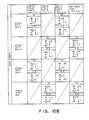
- FIG. 29 is a block diagram illustrating a structural arrangement of an embodiment of the display apparatus according to the present invention.
- a display panel 801 is composed of scanning electrodes 802, data electrodes 803 and a ferroelectric liquid crystal disposed therebetween. The orientation of the ferroelectric liquid crystal is controlled by an electric field at each intersection of the scanning electrodes and data electrodes formed due to voltages applied across the electrodes.
- the display apparatus includes a data electrode driver circuit 804, which in turn comprises an image data shift register 8041 for storing image data serially supplied from a data signal line 806, a line memory 8042 for storing image data supplied in parallel from the image data shift register 8041, a data electrode driver 8043 for supplying voltages to data electrodes 803 according to the image data stored in the line memory 8042, and a data side power supply changeover unit 8044 for changing over among voltages V D , 0 and -V D supplied to the data electrodes 803 based on a signal from a changeover control line 811.
- a data electrode driver circuit 804 which in turn comprises an image data shift register 8041 for storing image data serially supplied from a data signal line 806, a line memory 8042 for storing image data supplied in parallel from the image data shift register 8041, a data electrode driver 8043 for supplying voltages to data electrodes 803 according to the image data stored in the line memory 8042, and a data side power supply changeover unit 8044 for changing over among voltages
- the display apparatus further includes a scanning electrode driver circuit 805, which in turn comprises a decoder 8051 for designating a scanning electrode among all the scanning electrodes based on a signal received from a scanning address data line 807, a scanning electrode driver 8052 for applying voltages to the scanning electrodes 802 based on a signal from the decoder 8051, and a scanning side power supply changeover unit 8053 for changing over among voltages V S , 0 and -V S supplied to the scanning electrodes 802 based on a signal from a changeover control line 811.
- a scanning electrode driver circuit 805 which in turn comprises a decoder 8051 for designating a scanning electrode among all the scanning electrodes based on a signal received from a scanning address data line 807, a scanning electrode driver 8052 for applying voltages to the scanning electrodes 802 based on a signal from the decoder 8051, and a scanning side power supply changeover unit 8053 for changing over among voltages V S , 0 and -V S supplied to the scanning
- the display apparatus further includes a CPU 808, which receives clock pulses from an oscillator 809, controls the image memory 810, and controls the signal transfer over the data signal line 806, scanning address data line 807 and changeover control line 811.
- a CPU 808 which receives clock pulses from an oscillator 809, controls the image memory 810, and controls the signal transfer over the data signal line 806, scanning address data line 807 and changeover control line 811.
- ferroelectric liquid crystal showing bistability used in the present invention chiral smectic liquid crystals having ferroelectricity are most preferred.
- a liquid crystal in chiral smectic C phase (SmC*) or H phase (SmH*) is particularly suited.
- ferroelectric liquid crystals are described in, e.g., "LE JOURNAL DE PHYSIQUE LETTERS” 36 (L-69), 1975 "Ferroelectric Liquid Crystals”; “Applied Physics Letters” 36 (11) 1980, “Submicro-Second Bistable Electrooptic Switching in Liquid Crystals”; “Kotai Butsuri (Solid State Physics)” 16 (141), 1981 “Liquid Crystal”; U.S. Patents Nos. 4556727, 4561726, 4614609, 4589996 and 4592858. Ferroelectric liquid crystals disclosed in these publications may be used in the present invention.
- ferroelectric liquid crystal compound used in the present invention are decyloxybenzylidene-p′-amino-2-methylbutylcinnamate (DOBAMBC), hexyloxybenzylidene-p′-amino-2-chloropropylcinnamate (HOBACPC), 4-O-(2-methyl)butylresorcilidene-4′-octylaniline (MBRA 8), etc.
- DOBAMBC decyloxybenzylidene-p′-amino-2-methylbutylcinnamate
- HOBACPC hexyloxybenzylidene-p′-amino-2-chloropropylcinnamate
- MBRA 8 4-O-(2-methyl)butylresorcilidene-4′-octylaniline
- the device When a device is constituted by using these materials, the device may be supported with a block of copper, etc. in which a heater is embedded in order to realize a temperature condition where the liquid crystal compounds assume an SmC*- or SmH*-phase.
- ferroelectric liquid crystal in chiral smectic F phase, I phase, G phase or K phase in addition to the above mentioned SmC* and SmH* phases.
- Reference numerals 301a and 301b denote substrates (glass plates) on which a transparent electrode of, e.g., In2O3, SnO2, ITO (Indium-Tin-Oxide), etc., is disposed, respectively.
- a liquid crystal of an SmC*-phase in which liquid crystal molecular layers 302 are oriented perpendicular to surfaces of the glass plates is hermetically disposed therebetween.
- a full line 303 shows liquid crystal molecules.
- Each liquid crystal molecule 303 has a dipole moment (P ⁇ ) 304 in a direction perpendicular to the axis thereof.
- liquid crystal molecules 303 When a voltage higher than a certain threshold level is applied between electrodes formed on the base plates 301a and 301b, a helical or spiral structure of the liquid crystal molecule 303 is unwound or released to change the alignment direction of respective liquid crystal molecules 303 so that the dipole moment (P ⁇ ) 304 are all directed in the direction of the electric field.
- the liquid crystal molecules 303 have an elongated shape and show refractive anisotropy between the long axis and the short axis thereof.
- the liquid crystal cell when, for instance, polarizers arranged in a cross nicol relationship, i.e., with their polarizing directions crossing each other, are disposed on the upper and the lower surfaces of the glass plates, the liquid crystal cell thus arranged functions as a liquid crystal optical modulation device of which optical characteristics vary depending upon the polarity of an applied voltage.
- the thickness of the liquid crystal cell is sufficiently thin (e.g., 1 micron)
- the helical structure of the liquid crystal molecules is released without application of an electric field whereby the dipole moment assumes either of the two states, i.e., Pa in an upper direction 314a or Pb in a lower direction 314b, thus providing a bistability condition, as shown in Figure 31.
- the dipole moment is directed either in the upper direction 314a or in the lower direction 314b depending on the vector of the electric field Ea or Eb.
- the liquid crystal molecules are oriented to either a first orientation state 313a or a second orientation state 313b.
- the response speed is quite fast.
- Second is that the orientation of the liquid crystal shows bistability.
- the second advantage will be further explained, e.g., with reference to Figure 31.
- the electric field Ea is applied to the liquid crystal molecules, they are oriented in the first stable state 313a. This state is stably retained even if the electric field is removed.
- the electric field Eb of which direction is opposite to that of the electric field Ea is applied thereto, the liquid crystal molecules are oriented to the second orientation state 313b, whereby the directions of molecules are changed. Likewise, the latter state is stably retained even if the electric field is removed.
- the liquid crystal molecules are placed in the respective orientation states.
- the thickness of the cell is as thin as possible and generally 0.5 to 20 microns, particularly 1 to 5 microns.
- the present invention it is possible to suppress the occurrence of flickering even in a low frame frequency driving at a low temperature, thus providing an improved display quality. According to another aspect of the above effect, it has become possible to realize a high-quality display free from flickering over a wide temperature range ranging from a low temperature to a high temperature.
- the present invention further realizes a gradational display with suppression of flickering caused by scanning drive at a low frequency.
- the present invention it is also possible to have a large drive margin and provide a constant contrast. Particularly, it is possible to prevent the occurrence of a pale black background stripe pattern and provide a high-quality display free from image flow.
- a liquid crystal apparatus comprises a) a liquid crystal device comprising an electrode matrix composed of scanning electrodes and data electrodes, and a ferroelectric liquid crystal; and b) a driving means.
- the driving means includes a first drive means for applying a scanning selection signal two or more scanning electrodes apart in one vertical scanning so at to effect in one picture scanning in plural times of vertical scanning, and a second drive means for applying data signals in synchronism with the scanning selection signal.
Landscapes
- Physics & Mathematics (AREA)
- Engineering & Computer Science (AREA)
- General Physics & Mathematics (AREA)
- Chemical & Material Sciences (AREA)
- Crystallography & Structural Chemistry (AREA)
- Nonlinear Science (AREA)
- Computer Hardware Design (AREA)
- Theoretical Computer Science (AREA)
- Mathematical Physics (AREA)
- Optics & Photonics (AREA)
- Geometry (AREA)
- Liquid Crystal Display Device Control (AREA)
- Liquid Crystal (AREA)
- Liquid Crystal Substances (AREA)
- Physical Or Chemical Processes And Apparatus (AREA)
Priority Applications (1)
| Application Number | Priority Date | Filing Date | Title |
|---|---|---|---|
| EP94104881A EP0606929B1 (fr) | 1987-11-12 | 1988-11-10 | Dispositif à cristaux liquides |
Applications Claiming Priority (6)
| Application Number | Priority Date | Filing Date | Title |
|---|---|---|---|
| JP287172/87 | 1987-11-12 | ||
| JP62287172A JP2632878B2 (ja) | 1987-11-12 | 1987-11-12 | 表示装置のマルチプレキシング駆動法 |
| JP1531/88 | 1988-01-06 | ||
| JP153188A JP2656053B2 (ja) | 1988-01-06 | 1988-01-06 | 液晶装置 |
| JP26671588A JP2575196B2 (ja) | 1988-10-21 | 1988-10-21 | 表示装置の駆動法 |
| JP266715/88 | 1988-10-21 |
Related Child Applications (2)
| Application Number | Title | Priority Date | Filing Date |
|---|---|---|---|
| EP94104881.1 Division-Into | 1988-11-10 | ||
| EP94104881A Division EP0606929B1 (fr) | 1987-11-12 | 1988-11-10 | Dispositif à cristaux liquides |
Publications (3)
| Publication Number | Publication Date |
|---|---|
| EP0316774A2 true EP0316774A2 (fr) | 1989-05-24 |
| EP0316774A3 EP0316774A3 (fr) | 1992-03-04 |
| EP0316774B1 EP0316774B1 (fr) | 1997-01-29 |
Family
ID=27274959
Family Applications (2)
| Application Number | Title | Priority Date | Filing Date |
|---|---|---|---|
| EP88118766A Expired - Lifetime EP0316774B1 (fr) | 1987-11-12 | 1988-11-10 | Appareil à cristaux à cristaux liquides |
| EP94104881A Expired - Lifetime EP0606929B1 (fr) | 1987-11-12 | 1988-11-10 | Dispositif à cristaux liquides |
Family Applications After (1)
| Application Number | Title | Priority Date | Filing Date |
|---|---|---|---|
| EP94104881A Expired - Lifetime EP0606929B1 (fr) | 1987-11-12 | 1988-11-10 | Dispositif à cristaux liquides |
Country Status (7)
| Country | Link |
|---|---|
| US (4) | US5058994A (fr) |
| EP (2) | EP0316774B1 (fr) |
| KR (1) | KR920010052B1 (fr) |
| AT (2) | ATE201788T1 (fr) |
| AU (1) | AU609901B2 (fr) |
| DE (2) | DE3855777T2 (fr) |
| ES (1) | ES2099061T3 (fr) |
Cited By (13)
| Publication number | Priority date | Publication date | Assignee | Title |
|---|---|---|---|---|
| EP0433540A3 (en) * | 1989-12-19 | 1991-11-27 | Canon Kabushiki Kaisha | Information processing apparatus and display system |
| EP0434042A3 (en) * | 1989-12-20 | 1992-06-24 | Canon Kabushiki Kaisha | Display apparatus |
| EP0487045A3 (en) * | 1990-11-21 | 1993-01-07 | Canon Kabushiki Kaisha | Liquid crystal apparatus and method of driving the same |
| US5208689A (en) * | 1990-09-13 | 1993-05-04 | U.S. Philips Corporation | Electro-optic display device with increased number of transmission levels |
| FR2694118A1 (fr) * | 1992-07-24 | 1994-01-28 | Fujitsu Ltd | Dispositif de panneau d'affichage à plasma et son procédé d'activation. |
| WO1994008329A1 (fr) * | 1992-10-03 | 1994-04-14 | Central Research Laboratories Limited | Adressage d'une cellule a cristaux liquides du type matriciel |
| US5347393A (en) * | 1991-11-19 | 1994-09-13 | U.S. Philips Corporation | Electro-optical display device with sub-electrodes |
| US5404236A (en) * | 1990-04-20 | 1995-04-04 | U.S. Philips Corporation | Display device with crossing electrodes with specific ratio for gray scale |
| EP0703562A2 (fr) * | 1994-09-26 | 1996-03-27 | Canon Kabushiki Kaisha | Méthode et dispositif de commande d'un dispositif d'affichage |
| EP0703561A2 (fr) * | 1994-09-26 | 1996-03-27 | Canon Kabushiki Kaisha | Méthode et dispositif de commande d'un dispositif d'affichage |
| EP0492542B1 (fr) * | 1990-12-28 | 1996-06-05 | Sharp Kabushiki Kaisha | Méthode de commande d'affichage |
| EP0715293A3 (fr) * | 1990-04-06 | 1996-07-31 | Canon Kk | Dispositif d'affichage |
| EP0788014A3 (fr) * | 1996-02-01 | 1998-09-09 | Canon Kabushiki Kaisha | Appareil d'affichage pour l'affichage de niveaux de gris |
Families Citing this family (62)
| Publication number | Priority date | Publication date | Assignee | Title |
|---|---|---|---|---|
| US5227900A (en) * | 1990-03-20 | 1993-07-13 | Canon Kabushiki Kaisha | Method of driving ferroelectric liquid crystal element |
| US5757352A (en) * | 1990-06-18 | 1998-05-26 | Canon Kabushiki Kaisha | Image information control apparatus and display device |
| JP2761128B2 (ja) * | 1990-10-31 | 1998-06-04 | 富士通株式会社 | 液晶表示装置 |
| US5283564A (en) * | 1990-12-26 | 1994-02-01 | Canon Kabushiki Kaisha | Liquid crystal apparatus with temperature-dependent pulse manipulation |
| JP2826772B2 (ja) * | 1991-01-07 | 1998-11-18 | キヤノン株式会社 | 液晶表示装置 |
| JP3227197B2 (ja) * | 1991-06-18 | 2001-11-12 | キヤノン株式会社 | 表示装置 |
| JP2868650B2 (ja) * | 1991-07-24 | 1999-03-10 | キヤノン株式会社 | 表示装置 |
| JP3133107B2 (ja) * | 1991-08-28 | 2001-02-05 | キヤノン株式会社 | 表示装置 |
| JPH0580721A (ja) * | 1991-09-18 | 1993-04-02 | Canon Inc | 表示制御装置 |
| JP3171891B2 (ja) * | 1991-11-08 | 2001-06-04 | キヤノン株式会社 | 表示制御装置 |
| JPH05134626A (ja) * | 1991-11-11 | 1993-05-28 | Sharp Corp | 液晶素子とその駆動方法 |
| US5673062A (en) * | 1992-11-06 | 1997-09-30 | Canon Kabushiki Kaisha | Liquid crystal apparatus |
| US5815133A (en) * | 1992-11-17 | 1998-09-29 | Canon Kabushiki Kaisha | Display apparatus |
| JP3118682B2 (ja) * | 1992-12-25 | 2000-12-18 | キヤノン株式会社 | 液晶表示装置 |
| JP2942092B2 (ja) * | 1993-04-20 | 1999-08-30 | キヤノン株式会社 | 液晶素子の制御方法 |
| CA2137723C (fr) * | 1993-12-14 | 1996-11-26 | Canon Kabushiki Kaisha | Dispositif d'affichage |
| US5638195A (en) * | 1993-12-21 | 1997-06-10 | Canon Kabushiki Kaisha | Liquid crystal display device for improved halftone display |
| US5844538A (en) * | 1993-12-28 | 1998-12-01 | Sharp Kabushiki Kaisha | Active matrix-type image display apparatus controlling writing of display data with respect to picture elements |
| JP2942161B2 (ja) * | 1993-12-28 | 1999-08-30 | キヤノン株式会社 | 液晶の配向処理方法、該方法を用いた液晶素子の製造方法、並びに液晶素子 |
| GB2286153B (en) * | 1994-01-31 | 1997-05-14 | Neopost Ltd | Franking machine |
| JP3476241B2 (ja) | 1994-02-25 | 2003-12-10 | 株式会社半導体エネルギー研究所 | アクティブマトリクス型表示装置の表示方法 |
| WO1995034020A1 (fr) * | 1994-06-03 | 1995-12-14 | Seiko Epson Corporation | Procede de commande d'un dispositif d'affichage a cristaux liquides, dispositif d'affichage a cristaux liquides, appareil electronique et circuit de commande |
| US6545653B1 (en) * | 1994-07-14 | 2003-04-08 | Matsushita Electric Industrial Co., Ltd. | Method and device for displaying image signals and viewfinder |
| DE69524013T2 (de) * | 1994-09-12 | 2002-06-06 | Canon K.K., Tokio/Tokyo | Ansteuerung für eine Ferroelectrische Flüsigkristallvorichtung |
| US5739808A (en) * | 1994-10-28 | 1998-04-14 | Canon Kabushiki Kaisha | Display control method and apparatus |
| JP3058804B2 (ja) * | 1994-11-16 | 2000-07-04 | キヤノン株式会社 | 液晶装置 |
| US5883608A (en) * | 1994-12-28 | 1999-03-16 | Canon Kabushiki Kaisha | Inverted signal generation circuit for display device, and display apparatus using the same |
| US5808597A (en) * | 1995-03-08 | 1998-09-15 | Canon Kabushiki Kaisha | Illumination device for liquid crystal display apparatus |
| US5986736A (en) * | 1995-04-26 | 1999-11-16 | Canon Kabushiki Kaisha | Liquid crystal device, image display apparatus and image forming apparatus |
| US6229515B1 (en) * | 1995-06-15 | 2001-05-08 | Kabushiki Kaisha Toshiba | Liquid crystal display device and driving method therefor |
| GB9526270D0 (en) * | 1995-12-21 | 1996-02-21 | Secr Defence | Multiplex addressing of ferroelectric liquid crystal displays |
| GB2312542B (en) * | 1995-12-21 | 2000-02-23 | Secr Defence | Multiplex addressing of ferroelectric liquid crystal displays |
| US5999157A (en) * | 1995-12-27 | 1999-12-07 | Canon Kabushiki Kaisha | Suppressing liquid crystal movement based on the relationship between a display pattern and a driving waveform |
| JP3182070B2 (ja) * | 1996-01-16 | 2001-07-03 | キヤノン株式会社 | 液晶素子及び液晶素子の駆動方法 |
| US5956010A (en) * | 1996-05-31 | 1999-09-21 | Canon Kabushiki Kaisha | Liquid crystal apparatus and driving method |
| US6028579A (en) * | 1996-06-12 | 2000-02-22 | Canon Kabushiki Kaisha | Driving method for liquid crystal devices |
| JP3612895B2 (ja) * | 1996-10-23 | 2005-01-19 | カシオ計算機株式会社 | 液晶表示装置 |
| US6133894A (en) * | 1996-12-17 | 2000-10-17 | Canon Kabushiki Kaisha | Driving method for optical apparatus |
| JP3342341B2 (ja) * | 1997-03-13 | 2002-11-05 | キヤノン株式会社 | 液晶装置及び液晶装置の駆動方法 |
| US5730537A (en) * | 1997-03-13 | 1998-03-24 | Hewlett-Packard Company | Print media handling and ejection system |
| US6452581B1 (en) | 1997-04-11 | 2002-09-17 | Canon Kabushiki Kaisha | Driving method for liquid crystal device and liquid crystal apparatus |
| US6222517B1 (en) | 1997-07-23 | 2001-04-24 | Canon Kabushiki Kaisha | Liquid crystal apparatus |
| JPH1164823A (ja) | 1997-08-21 | 1999-03-05 | Denso Corp | マトリクス型液晶表示装置 |
| TW428158B (en) * | 1998-02-24 | 2001-04-01 | Nippon Electric Co | Method and device for driving liquid crystal display element |
| JP3347678B2 (ja) | 1998-06-18 | 2002-11-20 | キヤノン株式会社 | 液晶素子とその駆動方法 |
| JP3266191B2 (ja) * | 1998-12-25 | 2002-03-18 | 日本電気株式会社 | プラズマ・ディスプレイ、その画像表示方法 |
| US6670937B1 (en) | 1999-03-01 | 2003-12-30 | Canon Kabushiki Kaisha | Liquid crystal display apparatus |
| US6563482B1 (en) | 1999-07-21 | 2003-05-13 | Semiconductor Energy Laboratory Co., Ltd. | Display device |
| EP1296174B1 (fr) * | 2000-04-28 | 2016-03-09 | Sharp Kabushiki Kaisha | Unite d'affichage, procede d'excitation pour unite d'affichage, et appareil electronique de montage d'une unite d'affichage |
| EP1430938B1 (fr) * | 2002-11-20 | 2013-01-23 | Universal Entertainment Corporation | Automate de jeu et afficheur correspondant |
| US7986296B2 (en) * | 2004-05-24 | 2011-07-26 | Au Optronics Corporation | Liquid crystal display and its driving method |
| JP4561557B2 (ja) * | 2005-09-22 | 2010-10-13 | 株式会社デンソー | 液晶表示装置および車両周辺監視装置 |
| EP2149874A4 (fr) * | 2007-04-26 | 2011-11-30 | Sharp Kk | Ecran à cristaux liquides |
| JP4992969B2 (ja) * | 2007-04-27 | 2012-08-08 | 富士通株式会社 | 表示装置の駆動方法及び表示装置 |
| JP5675795B2 (ja) * | 2010-05-17 | 2015-02-25 | シャープ株式会社 | 液晶表示装置 |
| TW201227660A (en) * | 2010-12-22 | 2012-07-01 | Ind Tech Res Inst | Apparatus and method for driving multi-stable display panel |
| US8874390B2 (en) | 2011-03-23 | 2014-10-28 | Hach Company | Instrument and method for processing a doppler measurement signal |
| KR101988526B1 (ko) * | 2013-04-30 | 2019-06-12 | 엘지디스플레이 주식회사 | 저속 구동용 표시장치와 그 구동방법 |
| KR102035755B1 (ko) * | 2013-04-30 | 2019-11-08 | 엘지디스플레이 주식회사 | 저속 구동용 표시장치와 그 구동방법 |
| KR102050380B1 (ko) * | 2013-04-30 | 2019-11-29 | 엘지디스플레이 주식회사 | 저속 구동용 표시장치와 그 구동방법 |
| JP6428079B2 (ja) | 2013-11-08 | 2018-11-28 | セイコーエプソン株式会社 | 電気光学装置の駆動方法、電気光学装置、及び電子機器 |
| CN109064963A (zh) * | 2018-09-05 | 2018-12-21 | 京东方科技集团股份有限公司 | 显示装置及驱动方法、移位寄存器、驱动电路 |
Family Cites Families (25)
| Publication number | Priority date | Publication date | Assignee | Title |
|---|---|---|---|---|
| US4367924A (en) * | 1980-01-08 | 1983-01-11 | Clark Noel A | Chiral smectic C or H liquid crystal electro-optical device |
| JPH0629919B2 (ja) * | 1982-04-16 | 1994-04-20 | 株式会社日立製作所 | 液晶素子の駆動方法 |
| US4452785A (en) * | 1982-11-08 | 1984-06-05 | Malette William Graham | Method for the therapeutic occlusion |
| JPS59129837A (ja) * | 1983-01-14 | 1984-07-26 | Canon Inc | 時分割電圧印加方法及び装置 |
| JPH07118794B2 (ja) * | 1983-03-16 | 1995-12-18 | シチズン時計株式会社 | 表示装置 |
| US4655561A (en) * | 1983-04-19 | 1987-04-07 | Canon Kabushiki Kaisha | Method of driving optical modulation device using ferroelectric liquid crystal |
| JPS59221183A (ja) * | 1983-05-31 | 1984-12-12 | Seiko Epson Corp | 液晶表示式受像装置の駆動方式 |
| AU584867B2 (en) * | 1983-12-09 | 1989-06-08 | Seiko Instruments & Electronics Ltd. | A liquid crystal display device |
| JPS60142326A (ja) * | 1983-12-29 | 1985-07-27 | Matsushita Electric Ind Co Ltd | 液晶表示装置 |
| DE3400009A1 (de) * | 1984-01-02 | 1985-07-11 | Henkel KGaA, 4000 Düsseldorf | Entschaeumer fuer waessrige dispersionen und loesungen von kunstharzen |
| US4701799A (en) * | 1984-03-13 | 1987-10-20 | Sharp Kabushiki Kaisha | Image display panel drive |
| JPS60257497A (ja) * | 1984-06-01 | 1985-12-19 | シャープ株式会社 | 液晶表示装置の駆動方法 |
| JPS60257683A (ja) * | 1984-06-01 | 1985-12-19 | Sharp Corp | 液晶表示装置の駆動回路 |
| JPS6186732A (ja) * | 1984-10-04 | 1986-05-02 | Canon Inc | 液晶装置 |
| JPS61114669A (ja) * | 1984-11-09 | 1986-06-02 | Sanyo Electric Co Ltd | 液晶表示装置 |
| GB2173336B (en) * | 1985-04-03 | 1988-04-27 | Stc Plc | Addressing liquid crystal cells |
| US4778260A (en) * | 1985-04-22 | 1988-10-18 | Canon Kabushiki Kaisha | Method and apparatus for driving optical modulation device |
| JPS61272724A (ja) * | 1985-05-27 | 1986-12-03 | Seiko Epson Corp | 液晶表示装置 |
| US4816816A (en) * | 1985-06-17 | 1989-03-28 | Casio Computer Co., Ltd. | Liquid-crystal display apparatus |
| GB2185614B (en) * | 1985-12-25 | 1990-04-18 | Canon Kk | Optical modulation device |
| JPH0827601B2 (ja) * | 1986-01-13 | 1996-03-21 | 株式会社日立製作所 | 液晶表示装置、及びその駆動方法 |
| GB2173629B (en) * | 1986-04-01 | 1989-11-15 | Stc Plc | Addressing liquid crystal cells |
| DE3850520T2 (de) * | 1987-03-31 | 1994-12-01 | Canon Kk | Anzeigevorrichtung. |
| EP0291252A3 (fr) * | 1987-05-12 | 1989-08-02 | Seiko Epson Corporation | Procédé et dispositif d'affichage vidéo |
| FR2615644B1 (fr) * | 1987-05-18 | 1989-06-30 | Brunel Christian | Dispositif d'affichage electroluminescent a effet memoire et a demi-teintes |
-
1988
- 1988-11-10 AT AT94104881T patent/ATE201788T1/de not_active IP Right Cessation
- 1988-11-10 DE DE3855777T patent/DE3855777T2/de not_active Expired - Fee Related
- 1988-11-10 DE DE3856474T patent/DE3856474T2/de not_active Expired - Fee Related
- 1988-11-10 EP EP88118766A patent/EP0316774B1/fr not_active Expired - Lifetime
- 1988-11-10 AT AT88118766T patent/ATE148573T1/de not_active IP Right Cessation
- 1988-11-10 ES ES88118766T patent/ES2099061T3/es not_active Expired - Lifetime
- 1988-11-10 EP EP94104881A patent/EP0606929B1/fr not_active Expired - Lifetime
- 1988-11-11 AU AU25074/88A patent/AU609901B2/en not_active Ceased
- 1988-11-12 KR KR1019880014884A patent/KR920010052B1/ko not_active Expired
- 1988-11-14 US US07/271,240 patent/US5058994A/en not_active Expired - Lifetime
-
1994
- 1994-03-31 US US08/220,572 patent/US5506601A/en not_active Expired - Fee Related
-
1995
- 1995-05-25 US US08/450,217 patent/US5777592A/en not_active Expired - Fee Related
- 1995-05-25 US US08/450,025 patent/US5818408A/en not_active Expired - Fee Related
Cited By (20)
| Publication number | Priority date | Publication date | Assignee | Title |
|---|---|---|---|---|
| US5408247A (en) * | 1989-12-19 | 1995-04-18 | Canon Kabushiki Kaisha | Information processing apparatus and display system with simultaneous partial rewriting scanning capability |
| EP0433540A3 (en) * | 1989-12-19 | 1991-11-27 | Canon Kabushiki Kaisha | Information processing apparatus and display system |
| EP0434042A3 (en) * | 1989-12-20 | 1992-06-24 | Canon Kabushiki Kaisha | Display apparatus |
| US5172105A (en) * | 1989-12-20 | 1992-12-15 | Canon Kabushiki Kaisha | Display apparatus |
| EP0715293A3 (fr) * | 1990-04-06 | 1996-07-31 | Canon Kk | Dispositif d'affichage |
| US5754153A (en) * | 1990-04-06 | 1998-05-19 | Canon Kabushiki Kaisha | Display apparatus |
| US5404236A (en) * | 1990-04-20 | 1995-04-04 | U.S. Philips Corporation | Display device with crossing electrodes with specific ratio for gray scale |
| US5208689A (en) * | 1990-09-13 | 1993-05-04 | U.S. Philips Corporation | Electro-optic display device with increased number of transmission levels |
| EP0478043B1 (fr) * | 1990-09-13 | 1995-06-14 | Koninklijke Philips Electronics N.V. | Ecran de visualisation |
| EP0487045A3 (en) * | 1990-11-21 | 1993-01-07 | Canon Kabushiki Kaisha | Liquid crystal apparatus and method of driving the same |
| US5796380A (en) * | 1990-11-21 | 1998-08-18 | Canon Kabushiki Kaisha | Liquid crystal apparatus and method of driving same |
| EP0492542B1 (fr) * | 1990-12-28 | 1996-06-05 | Sharp Kabushiki Kaisha | Méthode de commande d'affichage |
| US5347393A (en) * | 1991-11-19 | 1994-09-13 | U.S. Philips Corporation | Electro-optical display device with sub-electrodes |
| FR2694118A1 (fr) * | 1992-07-24 | 1994-01-28 | Fujitsu Ltd | Dispositif de panneau d'affichage à plasma et son procédé d'activation. |
| US5629718A (en) * | 1992-10-03 | 1997-05-13 | Central Research Laboratories Limited | Addressing a matrix-type liquid crystal cell |
| WO1994008329A1 (fr) * | 1992-10-03 | 1994-04-14 | Central Research Laboratories Limited | Adressage d'une cellule a cristaux liquides du type matriciel |
| EP0703561A2 (fr) * | 1994-09-26 | 1996-03-27 | Canon Kabushiki Kaisha | Méthode et dispositif de commande d'un dispositif d'affichage |
| EP0703562A2 (fr) * | 1994-09-26 | 1996-03-27 | Canon Kabushiki Kaisha | Méthode et dispositif de commande d'un dispositif d'affichage |
| EP0788014A3 (fr) * | 1996-02-01 | 1998-09-09 | Canon Kabushiki Kaisha | Appareil d'affichage pour l'affichage de niveaux de gris |
| US6072555A (en) * | 1996-02-01 | 2000-06-06 | Canon Kabushiki Kaisha | Display apparatus capable of gradational display |
Also Published As
| Publication number | Publication date |
|---|---|
| DE3856474D1 (de) | 2001-07-05 |
| AU609901B2 (en) | 1991-05-09 |
| US5058994A (en) | 1991-10-22 |
| EP0606929B1 (fr) | 2001-05-30 |
| KR890008595A (ko) | 1989-07-12 |
| US5777592A (en) | 1998-07-07 |
| ATE148573T1 (de) | 1997-02-15 |
| EP0316774A3 (fr) | 1992-03-04 |
| ATE201788T1 (de) | 2001-06-15 |
| EP0606929A2 (fr) | 1994-07-20 |
| US5506601A (en) | 1996-04-09 |
| KR920010052B1 (ko) | 1992-11-13 |
| ES2099061T3 (es) | 1997-05-16 |
| DE3856474T2 (de) | 2001-11-08 |
| EP0606929A3 (fr) | 1995-01-11 |
| AU2507488A (en) | 1989-06-08 |
| EP0316774B1 (fr) | 1997-01-29 |
| DE3855777T2 (de) | 1997-06-26 |
| DE3855777D1 (de) | 1997-03-13 |
| US5818408A (en) | 1998-10-06 |
Similar Documents
| Publication | Publication Date | Title |
|---|---|---|
| EP0606929B1 (fr) | Dispositif à cristaux liquides | |
| EP0281160B1 (fr) | Dispositif à cristaux liquides | |
| US5602562A (en) | Liquid crystal apparatus and driving method | |
| EP0658870B1 (fr) | Dispositif d'affichage à niveaux de gris | |
| US4836656A (en) | Driving method for optical modulation device | |
| US4932759A (en) | Driving method for optical modulation device | |
| US4763994A (en) | Method and apparatus for driving ferroelectric liquid crystal optical modulation device | |
| KR0148246B1 (ko) | 액정 장치의 구동 방법 | |
| US4925277A (en) | Method and apparatus for driving optical modulation device | |
| US5734367A (en) | Liquid crystal apparatus | |
| US5440412A (en) | Driving method for a ferroelectric optical modulation device | |
| US4927243A (en) | Method and apparatus for driving optical modulation device | |
| EP0607598B1 (fr) | Méthode et dispositif pour un panneau d'affichage à cristaux liquides | |
| US5973657A (en) | Liquid crystal display apparatus | |
| US5815130A (en) | Chiral smectic liquid crystal display and method of selectively driving the scanning and data electrodes | |
| JPH05303076A (ja) | 液晶装置 | |
| AU621252B2 (en) | Liquid crystal apparatus | |
| JP2578490B2 (ja) | 表示装置の駆動法 | |
| JP2637517B2 (ja) | 液晶装置 | |
| JP2575196B2 (ja) | 表示装置の駆動法 | |
| JPH07109457B2 (ja) | 液晶装置 | |
| JPH063503B2 (ja) | 表示装置 | |
| JPH06258617A (ja) | 液晶表示素子の駆動方法 | |
| JPH06337403A (ja) | 液晶素子の駆動方法 | |
| JPH01177516A (ja) | 液晶装置 |
Legal Events
| Date | Code | Title | Description |
|---|---|---|---|
| PUAI | Public reference made under article 153(3) epc to a published international application that has entered the european phase |
Free format text: ORIGINAL CODE: 0009012 |
|
| 17P | Request for examination filed |
Effective date: 19881110 |
|
| AK | Designated contracting states |
Kind code of ref document: A2 Designated state(s): AT BE CH DE ES FR GB GR IT LI LU NL SE |
|
| PUAL | Search report despatched |
Free format text: ORIGINAL CODE: 0009013 |
|
| AK | Designated contracting states |
Kind code of ref document: A3 Designated state(s): AT BE CH DE ES FR GB GR IT LI LU NL SE |
|
| 17Q | First examination report despatched |
Effective date: 19930916 |
|
| GRAG | Despatch of communication of intention to grant |
Free format text: ORIGINAL CODE: EPIDOS AGRA |
|
| GRAH | Despatch of communication of intention to grant a patent |
Free format text: ORIGINAL CODE: EPIDOS IGRA |
|
| GRAH | Despatch of communication of intention to grant a patent |
Free format text: ORIGINAL CODE: EPIDOS IGRA |
|
| GRAA | (expected) grant |
Free format text: ORIGINAL CODE: 0009210 |
|
| AK | Designated contracting states |
Kind code of ref document: B1 Designated state(s): AT BE CH DE ES FR GB GR IT LI LU NL SE |
|
| DX | Miscellaneous (deleted) | ||
| PG25 | Lapsed in a contracting state [announced via postgrant information from national office to epo] |
Ref country code: IT Free format text: LAPSE BECAUSE OF FAILURE TO SUBMIT A TRANSLATION OF THE DESCRIPTION OR TO PAY THE FEE WITHIN THE PRESCRIBED TIME-LIMIT;WARNING: LAPSES OF ITALIAN PATENTS WITH EFFECTIVE DATE BEFORE 2007 MAY HAVE OCCURRED AT ANY TIME BEFORE 2007. THE CORRECT EFFECTIVE DATE MAY BE DIFFERENT FROM THE ONE RECORDED. Effective date: 19970129 Ref country code: LI Effective date: 19970129 Ref country code: AT Effective date: 19970129 Ref country code: BE Effective date: 19970129 Ref country code: CH Effective date: 19970129 Ref country code: GR Free format text: LAPSE BECAUSE OF FAILURE TO SUBMIT A TRANSLATION OF THE DESCRIPTION OR TO PAY THE FEE WITHIN THE PRESCRIBED TIME-LIMIT Effective date: 19970129 |
|
| REF | Corresponds to: |
Ref document number: 148573 Country of ref document: AT Date of ref document: 19970215 Kind code of ref document: T |
|
| REG | Reference to a national code |
Ref country code: CH Ref legal event code: EP |
|
| REF | Corresponds to: |
Ref document number: 3855777 Country of ref document: DE Date of ref document: 19970313 |
|
| ET | Fr: translation filed | ||
| REG | Reference to a national code |
Ref country code: ES Ref legal event code: FG2A Ref document number: 2099061 Country of ref document: ES Kind code of ref document: T3 |
|
| REG | Reference to a national code |
Ref country code: CH Ref legal event code: PL |
|
| PG25 | Lapsed in a contracting state [announced via postgrant information from national office to epo] |
Ref country code: LU Free format text: LAPSE BECAUSE OF NON-PAYMENT OF DUE FEES Effective date: 19971110 |
|
| PLBE | No opposition filed within time limit |
Free format text: ORIGINAL CODE: 0009261 |
|
| STAA | Information on the status of an ep patent application or granted ep patent |
Free format text: STATUS: NO OPPOSITION FILED WITHIN TIME LIMIT |
|
| 26N | No opposition filed | ||
| REG | Reference to a national code |
Ref country code: GB Ref legal event code: IF02 |
|
| PGFP | Annual fee paid to national office [announced via postgrant information from national office to epo] |
Ref country code: GB Payment date: 20021106 Year of fee payment: 15 Ref country code: SE Payment date: 20021106 Year of fee payment: 15 |
|
| PGFP | Annual fee paid to national office [announced via postgrant information from national office to epo] |
Ref country code: FR Payment date: 20021108 Year of fee payment: 15 |
|
| PGFP | Annual fee paid to national office [announced via postgrant information from national office to epo] |
Ref country code: DE Payment date: 20021114 Year of fee payment: 15 |
|
| PGFP | Annual fee paid to national office [announced via postgrant information from national office to epo] |
Ref country code: ES Payment date: 20021127 Year of fee payment: 15 |
|
| PGFP | Annual fee paid to national office [announced via postgrant information from national office to epo] |
Ref country code: NL Payment date: 20021129 Year of fee payment: 15 |
|
| PG25 | Lapsed in a contracting state [announced via postgrant information from national office to epo] |
Ref country code: GB Free format text: LAPSE BECAUSE OF NON-PAYMENT OF DUE FEES Effective date: 20031110 |
|
| PG25 | Lapsed in a contracting state [announced via postgrant information from national office to epo] |
Ref country code: ES Free format text: LAPSE BECAUSE OF NON-PAYMENT OF DUE FEES Effective date: 20031111 Ref country code: SE Free format text: LAPSE BECAUSE OF NON-PAYMENT OF DUE FEES Effective date: 20031111 |
|
| PG25 | Lapsed in a contracting state [announced via postgrant information from national office to epo] |
Ref country code: NL Free format text: LAPSE BECAUSE OF NON-PAYMENT OF DUE FEES Effective date: 20040601 |
|
| PG25 | Lapsed in a contracting state [announced via postgrant information from national office to epo] |
Ref country code: DE Free format text: LAPSE BECAUSE OF NON-PAYMENT OF DUE FEES Effective date: 20040602 |
|
| EUG | Se: european patent has lapsed | ||
| GBPC | Gb: european patent ceased through non-payment of renewal fee |
Effective date: 20031110 |
|
| PG25 | Lapsed in a contracting state [announced via postgrant information from national office to epo] |
Ref country code: FR Free format text: LAPSE BECAUSE OF NON-PAYMENT OF DUE FEES Effective date: 20040730 |
|
| NLV4 | Nl: lapsed or anulled due to non-payment of the annual fee |
Effective date: 20040601 |
|
| REG | Reference to a national code |
Ref country code: FR Ref legal event code: ST |
|
| REG | Reference to a national code |
Ref country code: ES Ref legal event code: FD2A Effective date: 20031111 |