EP0318113A2 - Tube cathodique de visualisation - Google Patents
Tube cathodique de visualisation Download PDFInfo
- Publication number
- EP0318113A2 EP0318113A2 EP88202655A EP88202655A EP0318113A2 EP 0318113 A2 EP0318113 A2 EP 0318113A2 EP 88202655 A EP88202655 A EP 88202655A EP 88202655 A EP88202655 A EP 88202655A EP 0318113 A2 EP0318113 A2 EP 0318113A2
- Authority
- EP
- European Patent Office
- Prior art keywords
- cathode ray
- display system
- ray tube
- tube display
- faceplate
- Prior art date
- Legal status (The legal status is an assumption and is not a legal conclusion. Google has not performed a legal analysis and makes no representation as to the accuracy of the status listed.)
- Withdrawn
Links
Images




Classifications
-
- H—ELECTRICITY
- H01—ELECTRIC ELEMENTS
- H01J—ELECTRIC DISCHARGE TUBES OR DISCHARGE LAMPS
- H01J29/00—Details of cathode-ray tubes or of electron-beam tubes of the types covered by group H01J31/00
- H01J29/46—Arrangements of electrodes and associated parts for generating or controlling the ray or beam, e.g. electron-optical arrangement
- H01J29/56—Arrangements for controlling cross-section of ray or beam; Arrangements for correcting aberration of beam, e.g. due to lenses
-
- H—ELECTRICITY
- H01—ELECTRIC ELEMENTS
- H01J—ELECTRIC DISCHARGE TUBES OR DISCHARGE LAMPS
- H01J29/00—Details of cathode-ray tubes or of electron-beam tubes of the types covered by group H01J31/00
- H01J29/46—Arrangements of electrodes and associated parts for generating or controlling the ray or beam, e.g. electron-optical arrangement
- H01J29/70—Arrangements for deflecting ray or beam
- H01J29/72—Arrangements for deflecting ray or beam along one straight line or along two perpendicular straight lines
- H01J29/74—Deflecting by electric fields only
-
- H—ELECTRICITY
- H01—ELECTRIC ELEMENTS
- H01J—ELECTRIC DISCHARGE TUBES OR DISCHARGE LAMPS
- H01J31/00—Cathode ray tubes; Electron beam tubes
- H01J31/08—Cathode ray tubes; Electron beam tubes having a screen on or from which an image or pattern is formed, picked up, converted, or stored
- H01J31/10—Image or pattern display tubes, i.e. having electrical input and optical output; Flying-spot tubes for scanning purposes
- H01J31/12—Image or pattern display tubes, i.e. having electrical input and optical output; Flying-spot tubes for scanning purposes with luminescent screen
- H01J31/123—Flat display tubes
- H01J31/124—Flat display tubes using electron beam scanning
Definitions
- This invention relates to a cathode ray tube display system comprising an envelope including a substantially flat faceplate carrying a phosphor screen, means for producing an electron beam and directing the beam substantially parallel to the faceplace and means to deflect the beam towards the faceplace.
- the beam is deflected towards the faceplate over a short distance and therefore a low-energy beam (energy ⁇ 2.5 KeV) is used.
- a low energy electron beam is sensitive to ambient magnetic fields.
- a magnetic field having a direction parallel to the faceplate and transversely to the beam direction can cause deflection of the beam in a direction parallel to the faceplate, producing a deviation from the intended path of the beam and thereby a picture defect.
- An external magnetic shield could be fitted around the tube's envelope to alleviate these effects, but this is expensive and adds to the bulkiness and weight of the tube.
- a cathode ray tube display system of the kind mentioned in the opening paragraph is characterized in that a beam position control means is arranged to sense periodically during operation of the tube the position of the beam with respect to a predetermined position remote from the means for producing the electron beam and to control periodically further deflection means in accordance therewith so as to maintain the beam substantially at a desired position relative to said predetermined position.
- the display system according to the invention is able to correct automatically deviation in the position of the beam from a desired position. Because the position of the beam is monitored periodically, and operation of the further deflecting means varies appropriately to constrain the beam to a predetermined path, the beam position is, if necessary, adjusted periodically to maintain its desired position.
- the sensing means is positioned as to sense deviation of the beam from a plane substantially parallel to the faceplate.
- a deflection of the beam towards or away from the screen could result in the beam impinging upon the screen at the wrong place, thereby giving rise to a picture defect.
- Deviations as a result of magnetic fields in a direction orthogonal to the screen are less critical in this respect as the resulting beam deflection is within the intended plane of the beam.
- the further deflection means preferably comprises an electrostatic deflection arrangement, although magnetic deflection means could alternatively be used.
- the electrode arrangement may comprise a pair of electrodes disposed on opposite sides of the beam path.
- the sensing means may comprise sensor devices disposed above and below the predetermined plane substantially parallel to the faceplate.
- the sensing means is located outside the normal picture forming deflection range of the beam and the beam position control means is effective to deflect periodically the beam towards the sensing means.
- the sensing means is located outside the normal range, there is no interference with the picture-producing beam.
- the sensor means may comprise a set of two sensor devices situated on opposite sides respectively of a predetermined plane substantially parallel to the faceplate.
- the sensor devices are arranged in this manner so that when the beam is deflected beyond its normal range it impinges on one or other, or both, of the sensor devices, to produce response signal outputs from the sensor device or devices affected, indicating the position of the beam.
- the two sensor devices are positioned symmetrically with respect to the predetermined plane and spaced apart by a distance less than the diameter of the beam.
- the beam is overscanned and is in the desired plane, it impinges on both sensor devices producing equal responses therefrom.
- Operation of the control means in controlling the further deflection means is determined on the basis of the response signal outputs.
- the control means responds to the response signal outputs to energise the further deflection means upstream of the sensing means to return to or keep the beam at the desired position.
- the set of sensor devices comprises a pair of electrodes insulated from one another. Impingement of the electron beam on these electrodes causes a current flow and the relative current flow from their outputs is therefore dependent on the position of the beam in relation to the pair of electrodes.
- the two outputs are used to provide a difference signal in accordance with which energisation of the further deflection means is determined.
- the performance of the sensor electrodes is dependent on the potential of the surrounding tube structure.
- these electrodes are energised with a small positive bias.
- the electron beam is preferably turned hard on, for example by means of the application of a video "bright up" pulse to the electron beam producing means, when the beam is deflected towards the sensor means.
- An embodiment of the cathode ray display system is characterized in that it comprises such a reversing lens between the means for producing an electron beam and the faceplate, and in that the sensing means is located between the reversing lens and the electron beam producing means.
- This embodiment may further include means adjacent the electron beam producing means for scanning the beam in a plane substantially parallel to the faceplate and perpendicular to the beam direction, the further deflection means being situated between the electron beam producing means and this scanning means.
- sensing means comprises two sets of two sensor devices which are located adjacent opposite extremes of the range of scanning of the beam produced by the means for scanning the beam in a plane substantially parallel to the faceplate.
- More information about the scanning beam may then be gotten, for example information on twisting of the scanning beam, that is a rotation about a central axis extending parallel to the faceplate, or a deflection of the scanning beam within the scanning plane.
- the cathode ray display tube comprises a generally flat-walled rectangular envelope 12 including a glass faceplate 14. On the inside surface of the faceplate 14, there is a screen comprising a layer 16 of phosphor material covered by an aluminium backing electrode 18.
- the interior of the envelope 12 is divided by an internal partition 20 to form a front region 22 and a rear region 24.
- a planar electrode 26 is provided on a rear side of the partition 20. Carried on the inside of the rear wall of the envelope is a planar electrode 28 corresponding to the electrode 26.
- Means for producing a low-energy electron beam is situated in the rear region 24, said means being arranged to direct an electron beam 32 parallel to the faceplate 14 and comprising an electron gun 30.
- An electrostatic line deflector 34 in the form of two electrodes is spaced by a short distance from the electron gun and is arranged coaxially therewith. In operation, the line deflector 34 is energised to deflect the beam 32 in a plane parallel with the faceplate 14 to effect line scanning.
- a reversing lens 36 comprising a trough-like electrode 38 which is spaced above the partition 20.
- a deflection means On the front side of the partition 20 there is provided a deflection means.
- This means comprises plurality of laterally elongate, vertically spaced electrodes 42 which are selectively energised to provide frame deflection of the electron beam 32 onto the input side of a electron multiplier 44 extending parallel to, and spaced from, the screen 16.
- the electron beam having undergone current multiplication within the multiplier 44, is accelerated onto the phosphor screen 16 by means of a accelerating field established between the screen electrode 18 and the output side of the multiplier 44.
- a corrector electrode arrangement 37 Situated between the gun and the line deflector 34 in the tube according to the present invention is a corrector electrode arrangement 37 consisting of a pair of electrodes, one on each side of the beam path.
- the beam in the region between the line deflector 34 and the reversing lens 36 ideally should lie in a plane parallel with the screen 16 and intersecting the entrance of the reversing lens within its acceptance window, which is around midway between the electrode 26 at the upper end of the partition 20 and the downwardly extending side wall of the electrode 38.
- beam in line scanned by the deflector 34 symmetrically with respect to a central axis 33 over a normal scan angle range which varies over a field, the maximum being indicated at 35.
- the magnetic fields can have components Hx, Hy and Hz in x-, y- and z-directions where x, y and z are mutually orthogonal axes, as shown in Figures 3 and 4.
- a solid line denotes a desired trajectory of the beam 32 and a dotted line an unwanted trajectory caused by an Hx component.
- the display tube is, in accordance with the invention, provided with a means for controlling the position of the beam in the rear region 24 of the tube to maintain the position of the beam in that region in a plane substantially parallel to the faceplate 14, this predetermined plane being indicated by the dotted line in Figure 3.
- each sensor assembly consists of a pair of sensor electrodes 50A and 51A, and 50B and 51B respectively, the electrodes of each assembly being separated from one another by an insulative layer and being situated above and below, and symmetrically with respect to, a predetermined plane corresponding with the desired plane of the beam.
- the spacing between the pair of sensor electrodes of each sensor assembly is less than the width of the electron beam, for example, around one quarter of the beam diameter.
- the surfaces of the sensor electrodes facing the electron gun 30 are cup-shaped and roughened so as to trap electrons.
- Figure 5 shows a typical line scan waveform applied to the line deflector 34 during a succession of field periods, here shown as being of 20 ms duration.
- the normal line scan waveform is indicated at LS and the additional overscan voltage pulse signals applied to the deflector causing the beam to be deflected towards the sensor assemblies 50 and 51, in turn, are indicated at SR and SL respectively which occur during each convention field blanking period.
- VL represents the peak to peak amplitude of the overscan pulse signals.
- the overscan beam suffers in a similar fashion from magnetic fields as the normal beam and deflection suffered by the overscan beam is indicative of deflection suffered by the normal beam.
- the currents reaching the front and back sensor electrodes vary in accordance with the y-position of the electron beam.
- the performance of the system depends on the potential of the sensor electrodes relative to the surrounding tube structure.
- a small positive bias typically around 5 to 20V, provides acceptable results, causing secondary electrons generated at the sensor electrode surfaces to be returned to the sensor electrodes.
- the electrical currents produced from the two sensor electrodes are subtracted to give a difference signal, Vy.
- a plot of Vy against y position of the beam is shown in Figure 5.
- the point C is obtained when the beam is centred on a sensor assembly so that both electrodes thereof producing equal currents.
- the regions M and W occur when the beam completely misses the sensor assembly.
- the width of the sensor electrodes is chosen so that significant deflection of the beam is required for this to happen.
- the difference signals are used to control a variable voltage signal applied to the corrector electrode arrangement 37 so as to return or keep the beam to its correct position, that is, in the predetermined plane.
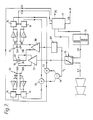
- FIG. 7 One embodiment of a circuit for achieving this is shown schematically in Figure 7 in which components already described are designated with the same reference number.
- a conventional line scan waveform, denoted LS, from a line scan generator (not shown) is applied to an input of an electronic switch 70 controlled by an output of a timing circuit 71 and thence to a drive amplifier 72 for application to the plates of the line deflector 34 to line scan the beam 32.
- the electronic switch 70 is also connected to a pulse generator 74 which generates the overscan pulse signals, OP, under the control of the timing circuit 71.
- the timing circuit is supplied with a conventional field synchronisation signals FS and during field blanking periods operates the electronic switch 70 so that the overscan pulse signals from generator 74 are supplied to the line deflector 34 via the drive amplifier 72 causing the beam to overscan towards the sensor assemblies 50 and 51.
- respective sample and hold circuits 76 are connected to the outputs from the individual sensor electrodes of the assemblies via associated amplifiers.
- the sample and hold circuits 76 are controlled by sample pulse waveforms S1 and S2 from timing circuit 71.
- the signals from the sensor electrodes 51A and 51B, that is, RB and RF, are sampled and held in the associated circuits 76. Thereafter, the beam is deflected onto the sensor assembly 50 and the process repeated.
- a control voltage is derived by means of drive amplifier 80 supplied with the output from subtractor 79, which is first filtered by a low pass filter 81, and supplied to the electrodes of electrode arrangement 37 to correct the position of the scanning beam relative to the sensor assemblies, and hence the reversing lens, and return it by movement in the y-direction to its desired position in the predetermined plane should it have been deflected away from this position by a magnetic field component Hx.
- a video "bright-up" pulse is used to turn the electron beam hard on for the periods it is directed towards the sensor assemblies so as to maximize the signal to noise ratio of the system.
- the beam position control circuit can be adapted to obtain correction signals for shifts of the beam in the x-direction and for rotation of the plane of the beam around an axis parallel to the z-axis, for example the axis 33, caused by magnetic field components.
- FIG. 9 there is shown schematically a modified part of the circuit of the beam position control system of Figure 7 in which output signals from the sensor assemblies 50 and 51 are processed in combination to provide error signals for x-direction and y-direction shifts and also for twist, that is, rotation about an axis parallel to the z-axis, indicated by angle S.
- Components corresponding with those of the circuit of Figure 7 have been designated with the same reference numbers.
- the outputs from respective pairs of the four sample and hold circuit 76 are added together and then the sums subtracted from one another to provide the y-direction error signal Vy, which is then used to control the deflector electrode arrangement 37 as previously.
- the x-direction error signal, Vx is derived by subtracting, in subtractor 82, the sum of the currents for both sensor electrodes of sensor assembly 50 obtained from adder 83 from the sum of the currents for both sensor electrodes of the sensor assembly 51 obtained from adder 84.
- the peak to peak amplitude of the overscan pulse signal, 0P supplied to the line deflector 34 during field blanking, indicated at VL in Figure 5, must be adjusted so that any x-direction shift of the scanning beam causes the current in one or other of the sensor assemblies to fall if it is to be sensed.
- the Vx signal may simply be fed into a shift input of the linescan drive amplifier 72 shown in Figure 7. This has the effect of biassing one of the plates of the line deflector 34 relative to the other by an amount which varies in accordance with the level of the error signal Vx so that the scanning beam downstream of the line deflector 34 is displaced in the x-direction and returned to the correct position where it is again symmetrical with respect to both the axis 33 and the sensor assemblies 50 and 51.
- the magnetic field causing this x-direction shift will also likely cause a further shift on the scanning beam during the remainder of its trajectory dowstream of the sensor assemblies and where it travels in the front region 22 of the tube parallel to the screen.
- This additional shifting will vary from top to bottom of the screen because of the different trajectory lengths involved so that the observed effect, provided the magnetic field is not too large, is both a shift and a parallelogram distortion of the displayed picture.
- the aforementioned technique can be used satisfactorily to reduce, but not eliminate completely, x-direction shift.
- FIG. 10 is a schematic representation of a modified form of part of the circuit of the beam position control system of Figures 7 and 9.
- the x-direction shift error signal Vx is derived in the manner described with reference to Figure 9. This signal is supplied to a low pass filter 90 whose output, here designated V1, is used to produce a shift in the switching voltages applied during the sensing period, (the field blanking period).
- V2 and V3 Two further voltages, V2 and V3, are derived from V1 by function generators 91 and 92 respectively.
- Voltage V2 provides a d.c. shift of the line scan signal so that the centre of the picture remains in the correct position while V3 is multiplied by the field modulation signal in the analog multiplier 94 used to modulate the line scan amplitude so as to provide correction for the parallellogram distortion mentioned above.
- Vf indicates the field ramp voltage waveform
- Vl indicates the line ramp voltage waveform
- V S is equal to (V3+Vl).Vf.K where K is a constant
- FB indicates the field blanking signal.
- the transfer functions used in the function generators 91 and 92 to derive V2 and V3 from V1 can be selected to suit the design of a particular tube and any magnetic shielding that may be present.
- Compensation for twisting of the scanning beam in a tube of this kind can be applied by taking a small fraction of the line scan waveform supplied to the line deflector 34 and feeding it, either directly or after inversion, as the case may be depending on the sense of twist, to the two electrodes of the corrector electrode arrangement 37.
- the amount of twist correction applied depends in this case on the amplitude of this signal.
- Automatic correction of twist can alternatively be achieved by using the twist error voltage signal, Vt in Figure 9, derived from the sensor assemblies by adding the outputs of sensors 50B and 51A, and 50A and 51B respectively in adders 85 and 86 and then subtracting the outputs therefrom in subtractor 87, to control the amplitude of the drive voltage applied to the two electrodes of the correcting electrode arrangement 37.
- the d.c. potential across these electrodes is still derived from the y-direction error signal, Vy.
- FIG. 11 and 12 another embodiment of a cathode ray tube display system according to the invention is shown.
- the display system 101 has means for generating a plurality of electron beams 102 which move at least substantially in a plane parallel to a front wall 103 and a rear wall 104 before they are deflected in the direction of a phosphor screen 105.
- the phosphor parts to be impinged on are selected via voltages at deflection electrodes 106 arranged in this embodiment on an insulative support 107.
- the electron beams 102 are deflected thereby towards the phosphor screen 105.
- the electron beams 102 are generated by means of semiconductor cathodes 108 which may be separately driven, having emissive surfaces 109 extending parallel to the walls 103, 104.
- the generated electron beams 102 are deflected through an angle of 90° by means of an electron-optical system 110.
- the structure and method of manufacture of a suitable electron-optical system is described in greater detail in the EP-A 0 284 119.
- the deflected electrons are subsequently accelerated in a direction parallel to the walls 103, 104 into a region 111.
- the display device 101 For each pixel column to be displayed the display device 101 comprises at least one cathode 108 which is provided with the correct voltages for obtaining the desired electron emission by means of a control unit 114 which is diagrammatically shown and which in turn is controlled by a circuit 113.
- the electrons of the beams 102 are accelerated parallel to the front and rear walls before they reach the actual display region. These electrons may deviate from their straight path under the influence of ambient magnetic fields.
- the display device 101 has beam position control means including sensor devices 115 situated opposite the means for producing the electron beam 110.
- Each or a selected number of beams can have associated therewith a respective set of sensors 115, or the device can comprise a single pair of sensors shared by some or all beams.
- the further deflection means may be formed by electrodes 116. Each beam can have a further deflection means associated therewith or the device can comprise a further deflection means shared by a group or all the electron beams. They may also be incorporated in the means for field deflecting the electron beams.
- the further deflection means comprise means to supply a bias voltage to the electrodes 106. The bias voltage is proportional to the shift ⁇ y and the energy of the accelerated electrons.
Landscapes
- Cathode-Ray Tubes And Fluorescent Screens For Display (AREA)
- Details Of Television Scanning (AREA)
Applications Claiming Priority (2)
| Application Number | Priority Date | Filing Date | Title |
|---|---|---|---|
| GB8727565 | 1987-11-25 | ||
| GB8727565A GB2213029A (en) | 1987-11-25 | 1987-11-25 | Beam position control in a flat crt display system |
Publications (2)
| Publication Number | Publication Date |
|---|---|
| EP0318113A2 true EP0318113A2 (fr) | 1989-05-31 |
| EP0318113A3 EP0318113A3 (fr) | 1989-09-13 |
Family
ID=10627505
Family Applications (1)
| Application Number | Title | Priority Date | Filing Date |
|---|---|---|---|
| EP88202655A Withdrawn EP0318113A3 (fr) | 1987-11-25 | 1988-11-24 | Tube cathodique de visualisation |
Country Status (3)
| Country | Link |
|---|---|
| EP (1) | EP0318113A3 (fr) |
| JP (1) | JPH01167939A (fr) |
| GB (1) | GB2213029A (fr) |
Family Cites Families (10)
| Publication number | Priority date | Publication date | Assignee | Title |
|---|---|---|---|---|
| US2630548A (en) * | 1937-12-04 | 1953-03-03 | Muller Egon Nicolas | Cathode-ray system |
| FR1587443A (fr) * | 1967-10-11 | 1970-03-20 | ||
| CH504821A (de) * | 1967-11-20 | 1971-03-15 | Eidophor Ag | Einrichtung zur Stabilisierung der Rasterlage und -grösse von mittels Kathodenstrahl zeilenweise auf getrennte Steuerschichten geschriebenen Bildern |
| DE3018453C2 (de) * | 1980-05-14 | 1982-05-06 | Standard Elektrik Lorenz Ag, 7000 Stuttgart | Verfahren zur Farbfernseh-Bilddarstellung und Farbbildröhre hierzu |
| GB2101396B (en) * | 1981-07-08 | 1985-05-22 | Philips Electronic Associated | Flat display tube |
| GB2139860B (en) * | 1983-05-09 | 1987-08-12 | Gen Electric Co Plc | Vibration compensated cathode ray tube display device |
| EP0135642A1 (fr) * | 1983-08-05 | 1985-04-03 | Deutsche ITT Industries GmbH | Système de détection pour tube image de télévision |
| EP0150903A3 (fr) * | 1984-01-04 | 1988-08-03 | Carroll Touch Technology, Inc. | Dispositif et méthode pour l'ajustage dynamique |
| EP0185674A1 (fr) * | 1984-05-11 | 1986-07-02 | Sri International | Affichage a panneau plat utilisant un reseau lineaire de cathodes d'emission de champ |
| JPH0821336B2 (ja) * | 1986-12-19 | 1996-03-04 | 松下電器産業株式会社 | 平板形陰極線管 |
-
1987
- 1987-11-25 GB GB8727565A patent/GB2213029A/en not_active Withdrawn
-
1988
- 1988-11-22 JP JP29372988A patent/JPH01167939A/ja active Pending
- 1988-11-24 EP EP88202655A patent/EP0318113A3/fr not_active Withdrawn
Also Published As
| Publication number | Publication date |
|---|---|
| GB2213029A (en) | 1989-08-02 |
| GB8727565D0 (en) | 1987-12-31 |
| EP0318113A3 (fr) | 1989-09-13 |
| JPH01167939A (ja) | 1989-07-03 |
Similar Documents
| Publication | Publication Date | Title |
|---|---|---|
| US4963789A (en) | Method and apparatus for dynamic magnetic field neutralization | |
| US4257023A (en) | Deflecting device for cathode-ray tube | |
| JPH067458B2 (ja) | 陰極線管とカラー表示装置 | |
| US3921025A (en) | Dual-beam CRT with vertical trace bowing correction means | |
| US6046713A (en) | Color display device including electron beam deflection arrangement for landing-correction | |
| EP0271926B1 (fr) | Dispositif de reproduction d'images comprenant un tube à rayons cathodiques de type plat | |
| EP0318113A2 (fr) | Tube cathodique de visualisation | |
| EP0292944A2 (fr) | Appareil à rayons cathodiques couleur comprenant des moyens de convergence dynamique | |
| EP0467332B1 (fr) | Appareil contenant un tube cathodique en couleurs | |
| US4853585A (en) | Display device with multiplicity of closely spaced electron beams | |
| US4216407A (en) | Flat panel display device with beam collector | |
| JPS5822854B2 (ja) | カデンリユウシソウサケンビキヨウ | |
| EP0281191A2 (fr) | Tube à rayons cathodiques plat | |
| EP0191596A2 (fr) | Procédé et dispositif de balayage d'un tube à rayons cathodiques à écran plat | |
| EP0198494B1 (fr) | Apparatus à rayons cathodiques couleur | |
| US4973889A (en) | Flat configuration cathode ray tube | |
| US2939981A (en) | Grid frame support structures for cathode ray tubes | |
| CA1174720A (fr) | Tube cathodique plat | |
| EP0651422B1 (fr) | Tube image en couleurs muni d'un blindage magnétique externe | |
| EP0660364A1 (fr) | Dispositif d'affichage avec unité de déflexion | |
| EP0115615B1 (fr) | Tube à rayons cathodiques plat avec dispositions pour la correction de défaut d'image trapéziforme | |
| EP0418962A1 (fr) | Dispositif de reproduction d'images et tube à rayons cathodiques | |
| US4746836A (en) | Flat cathode ray display tube | |
| US6545435B2 (en) | Cathode ray tube and signal detecting method in cathode ray tube | |
| US2945974A (en) | Electronic device |
Legal Events
| Date | Code | Title | Description |
|---|---|---|---|
| PUAI | Public reference made under article 153(3) epc to a published international application that has entered the european phase |
Free format text: ORIGINAL CODE: 0009012 |
|
| AK | Designated contracting states |
Kind code of ref document: A2 Designated state(s): DE FR GB IT |
|
| PUAL | Search report despatched |
Free format text: ORIGINAL CODE: 0009013 |
|
| RHK1 | Main classification (correction) |
Ipc: H01J 29/46 |
|
| AK | Designated contracting states |
Kind code of ref document: A3 Designated state(s): DE FR GB IT |
|
| STAA | Information on the status of an ep patent application or granted ep patent |
Free format text: STATUS: THE APPLICATION IS DEEMED TO BE WITHDRAWN |
|
| 18D | Application deemed to be withdrawn |
Effective date: 19900314 |