EP0318378B1 - Selbststabilisierter verriegelter Differentialkomparator mit nur einem Taktsignal - Google Patents
Selbststabilisierter verriegelter Differentialkomparator mit nur einem Taktsignal Download PDFInfo
- Publication number
- EP0318378B1 EP0318378B1 EP88402948A EP88402948A EP0318378B1 EP 0318378 B1 EP0318378 B1 EP 0318378B1 EP 88402948 A EP88402948 A EP 88402948A EP 88402948 A EP88402948 A EP 88402948A EP 0318378 B1 EP0318378 B1 EP 0318378B1
- Authority
- EP
- European Patent Office
- Prior art keywords
- transistor
- divergence
- transistors
- circuit
- differential
- Prior art date
- Legal status (The legal status is an assumption and is not a legal conclusion. Google has not performed a legal analysis and makes no representation as to the accuracy of the status listed.)
- Expired - Lifetime
Links
- 229920006395 saturated elastomer Polymers 0.000 claims description 8
- 230000000284 resting effect Effects 0.000 claims description 7
- 238000002955 isolation Methods 0.000 description 13
- 230000008878 coupling Effects 0.000 description 10
- 238000010168 coupling process Methods 0.000 description 10
- 238000005859 coupling reaction Methods 0.000 description 10
- 238000005259 measurement Methods 0.000 description 9
- 230000006641 stabilisation Effects 0.000 description 7
- 239000006185 dispersion Substances 0.000 description 4
- 238000011105 stabilization Methods 0.000 description 4
- 230000000295 complement effect Effects 0.000 description 3
- 238000010586 diagram Methods 0.000 description 3
- 238000005516 engineering process Methods 0.000 description 3
- 235000021183 entrée Nutrition 0.000 description 3
- 238000002347 injection Methods 0.000 description 3
- 239000007924 injection Substances 0.000 description 3
- 229910001218 Gallium arsenide Inorganic materials 0.000 description 2
- 230000003321 amplification Effects 0.000 description 2
- 230000007423 decrease Effects 0.000 description 2
- 238000003199 nucleic acid amplification method Methods 0.000 description 2
- 230000035945 sensitivity Effects 0.000 description 2
- 230000000087 stabilizing effect Effects 0.000 description 2
- 230000009471 action Effects 0.000 description 1
- 230000008859 change Effects 0.000 description 1
- 238000006243 chemical reaction Methods 0.000 description 1
- 230000000694 effects Effects 0.000 description 1
- 238000004519 manufacturing process Methods 0.000 description 1
- 239000000463 material Substances 0.000 description 1
- 230000007246 mechanism Effects 0.000 description 1
- 229910052710 silicon Inorganic materials 0.000 description 1
- 239000010703 silicon Substances 0.000 description 1
- 239000003381 stabilizer Substances 0.000 description 1
- 230000001629 suppression Effects 0.000 description 1
- 230000007704 transition Effects 0.000 description 1
Images

Classifications
-
- H—ELECTRICITY
- H03—ELECTRONIC CIRCUITRY
- H03K—PULSE TECHNIQUE
- H03K3/00—Circuits for generating electric pulses; Monostable, bistable or multistable circuits
- H03K3/02—Generators characterised by the type of circuit or by the means used for producing pulses
- H03K3/353—Generators characterised by the type of circuit or by the means used for producing pulses by the use, as active elements, of field-effect transistors with internal or external positive feedback
- H03K3/356—Bistable circuits
- H03K3/356017—Bistable circuits using additional transistors in the input circuit
- H03K3/356034—Bistable circuits using additional transistors in the input circuit the input circuit having a differential configuration
Definitions
- the present invention relates to an electronic circuit, lathe, self-stabilized differential comparator, with preamplification and with a single clock. Designed to operate at very high speed - in the microwave domain, up to several gigahertz - its unique clock, its self-stabilized resting voltages and its architecture make it very insensitive to technological dispersions in the manufacture of transistors, dispersions which cause measurement errors or instabilities.
- This comparator has been studied to be produced in integrated circuit on materials of group III-V such as GaAs, but of course it can also be produced, without departing from the scope of the invention, in silicon: its working speed is only less fast.
- Differential batch comparators use the positive reaction mechanism: the voltage difference between the inputs is found after amplification, on the outputs (Measurement phase). It is then that these signals are reinjected on the inputs (Divergence phase). Looping the outputs to the inputs leads to a rapid amplification of the voltage differences.
- FIG. 1 gives an example of an electrical diagram of a rocker comparator with nested differential stages, according to the art known
- the input signals E1 and E2, addressed to the gates of the transistors T6 and T7, are coupled with the output signals S1 and S2, taken from the gates of the transistors T8and T9, that is to say also on the drains of the transistors T6 and T7.
- This comparator comprises two nested differential stages: an internal stage T2 + T4 + T5 + T8 + T9 and an external stage T3 + T6 + T7 + T8 + T9.
- the transition from the measurement phase to the divergence phase is effected by switching the current from the external differential stage to the internal differential stage, by means of clocks and transistors T2 + T3, and the divergence begins.
- Level translators (T10, D1, D2, D3, T12) and (T11, D4, D5, D6, T13) are essential to compensate for the difference in rest levels existing between inputs and outputs
- This comparator now only has one clock, and takes technological imperfections into account by stabilizing the levels, but it does not include the isolation stage, hence the injection of charges during switching, with the disadvantages that it entails.
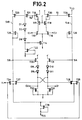
- the invention relates to a side differential differential comparator operating at very high frequencies, comprising a differential amplifier on the inputs of which the signals to be compared are applied, and a voltage level translator whose outputs deliver the output signals of the comparator and comprising between the input amplifier and the output translator, a divergence circuit in two branches symmetrical with respect to the outputs the amplifier, this divergence circuit comprising for each branch at least two transistors connected in series: a load transistor coupled by its gate to an output of the differential amplifier, and a loopback transistor coupled by its gate to an output of the level translator, characterized in that an isolation transistor is connected in series between the transistor load and the loopback transistor in each branch of the divergence circuit, the width of the grill e of the isolation transistor being intermediate between that of the load transistor and that of the single transistor current source for the two branches of the divergence circuit, so that the two isolation transistors cannot be saturated simultaneously, one of the two operating in resistive mode.
- the output O1 of the comparator is taken from the drain of transistor 33 of the level translator, and is simultaneously looped back onto the gate of the loop-back transistor T27, and the output O2, taken out of the drain of transistor T32 is looped back through the gate of T28 .
- the assembly is supplied between two analog voltages V DD and V SS , these voltages not all being shown in FIG. 2 for the sole purpose of not overloading it.
- the number of diodes, six in the self-locking loop, two in each level translator, is not limitative of the invention: it corresponds to a technology for making GaAs, but may differ depending on the technology implemented. These diodes can be replaced by resistors or transistors in technologies without diodes.
- SIA and SIB the intermediate outputs, between the coupling and isolation transistors, T23 and T25, T24 and T26, and SA and SB the intermediate outputs, applied to the level translators T31 and T31.
- All the transistors used in this assembly are of the normally conducting type, that is to say that they are conductive if no voltage is applied to their gate.
- the preamplification circuit amplifies the voltage difference between the two inputs E1 and E2.
- the signals present at outputs S1 and S2 of the differential preamplification stage are sent to the divergence stage thanks to an original coupling mode by the charge transistors T23 and T24 of the divergence stage. If the clock H is at low logic level, T27 and T28 are conductive, T34 and T35, are blocked, the divergence begins since the output signals are sent to the inputs of the divergence stage (grids of T27 and T28). After the divergence of SA and SB the circuit is brought back to equilibrium by placing the clock H at the high logic level, after which we can resume a divergence cycle.
- V (E1) - V (E2) G. (V (E1) - V (E2)).
- the gate-source voltage of T34 is equal to that of T35 and the current in the left branch is equal to that in the right branch.
- the gate-source voltages of T23 and T24 are therefore equal, so the difference VS1-VS2 is transferred between the points SIA and SIB.
- the self-control loop T21, D1 to D6, T22 has the role of stabilizing the resting voltages in S1 and S2 by enslavement of the current in T14, and thanks to the mode of coupling used between the preamplification circuit and the divergence state, and since it has been shown that in the measurement phase (clock in high state), the elements T23, T25, T34 as well as T24, T26 and T35 form two voltage followers, the rest voltages in SA and SB are imposed.
- the elements T30, D8, D9, T32 and T31, D10, D11, T33 also constitute tension followers, the rest levels of 01 and 02 are also imposed.
- the self-servo loop described above stabilizes all the resting voltages of the circuit.
- the input signals can no longer cause the system to reverse its decision before returning to the measurement phase.
Landscapes
- Manipulation Of Pulses (AREA)
- Amplifiers (AREA)
- Analogue/Digital Conversion (AREA)
Claims (6)
Applications Claiming Priority (2)
| Application Number | Priority Date | Filing Date | Title |
|---|---|---|---|
| FR8716465 | 1987-11-27 | ||
| FR8716465A FR2623952B1 (fr) | 1987-11-27 | 1987-11-27 | Comparateur differentiel a bascule autostabilise a horloge unique |
Publications (2)
| Publication Number | Publication Date |
|---|---|
| EP0318378A1 EP0318378A1 (de) | 1989-05-31 |
| EP0318378B1 true EP0318378B1 (de) | 1992-04-29 |
Family
ID=9357240
Family Applications (1)
| Application Number | Title | Priority Date | Filing Date |
|---|---|---|---|
| EP88402948A Expired - Lifetime EP0318378B1 (de) | 1987-11-27 | 1988-11-24 | Selbststabilisierter verriegelter Differentialkomparator mit nur einem Taktsignal |
Country Status (6)
| Country | Link |
|---|---|
| US (1) | US4975596A (de) |
| EP (1) | EP0318378B1 (de) |
| JP (1) | JPH01188121A (de) |
| CA (1) | CA1324641C (de) |
| DE (1) | DE3870588D1 (de) |
| FR (1) | FR2623952B1 (de) |
Families Citing this family (9)
| Publication number | Priority date | Publication date | Assignee | Title |
|---|---|---|---|---|
| US5041740A (en) * | 1990-04-30 | 1991-08-20 | Motorola, Inc. | Parallel clocked latch |
| US5121035A (en) * | 1991-02-27 | 1992-06-09 | Rockwell International Corporation | High speed gallium arsenide latch using depletion mode logic |
| US5184028A (en) * | 1992-06-15 | 1993-02-02 | Motorola, Inc. | Current compensating charge pump circuit |
| US5428307A (en) * | 1993-10-20 | 1995-06-27 | Silicon Systems, Inc. | Closed-loop peak detector topology |
| GB9417138D0 (en) | 1994-08-23 | 1994-10-12 | Discovision Ass | Data rate conversion |
| EP0834116B1 (de) * | 1995-06-09 | 2001-11-14 | Infineon Technologies AG | Schaltungsanordnung zum vergleich zweier elektrischer grössen |
| US8037371B1 (en) * | 2007-05-14 | 2011-10-11 | National Semiconductor Corporation | Apparatus and method for testing high-speed serial transmitters and other devices |
| US7809517B1 (en) | 2007-09-07 | 2010-10-05 | National Semiconductor Corporation | Apparatus and method for measuring phase noise/jitter in devices under test |
| US10686431B1 (en) * | 2019-10-18 | 2020-06-16 | Realtek Semiconductor Corp. | High-sensitivity clocked comparator and method thereof |
Family Cites Families (9)
| Publication number | Priority date | Publication date | Assignee | Title |
|---|---|---|---|---|
| US3540007A (en) * | 1967-10-19 | 1970-11-10 | Bell Telephone Labor Inc | Field effect transistor memory cell |
| DE2460146C3 (de) * | 1974-12-19 | 1981-11-05 | Ibm Deutschland Gmbh, 7000 Stuttgart | Bipolare Leseschaltung für integrierte Speichermatrix |
| JPS5938670B2 (ja) * | 1976-10-15 | 1984-09-18 | 日本電気株式会社 | 差信号増巾回路 |
| JPS5840918A (ja) * | 1981-09-03 | 1983-03-10 | Nec Corp | 電圧比較回路 |
| US4439694A (en) * | 1981-12-21 | 1984-03-27 | Gte Laboratories Incorporated | Comparator circuit |
| DE3442649A1 (de) * | 1984-11-22 | 1986-05-22 | Siemens AG, 1000 Berlin und 8000 München | Getakteter komparator fuer binaere signale sehr hoher bitrate |
| US4629911A (en) * | 1985-03-15 | 1986-12-16 | Tektronix, Inc. | Latching comparator |
| US4717838A (en) * | 1986-11-14 | 1988-01-05 | National Semiconductor Corporation | High input impedance, high gain CMOS strobed comparator |
| US4814648A (en) * | 1987-09-24 | 1989-03-21 | Texas Instruments Incorporated | Low 1/f noise amplifier for CCD imagers |
-
1987
- 1987-11-27 FR FR8716465A patent/FR2623952B1/fr not_active Expired - Fee Related
-
1988
- 1988-11-23 US US07/275,514 patent/US4975596A/en not_active Expired - Fee Related
- 1988-11-24 EP EP88402948A patent/EP0318378B1/de not_active Expired - Lifetime
- 1988-11-24 DE DE8888402948T patent/DE3870588D1/de not_active Expired - Fee Related
- 1988-11-25 CA CA000584236A patent/CA1324641C/en not_active Expired - Fee Related
- 1988-11-28 JP JP63298424A patent/JPH01188121A/ja active Pending
Also Published As
| Publication number | Publication date |
|---|---|
| CA1324641C (en) | 1993-11-23 |
| JPH01188121A (ja) | 1989-07-27 |
| EP0318378A1 (de) | 1989-05-31 |
| FR2623952A1 (fr) | 1989-06-02 |
| FR2623952B1 (fr) | 1991-11-29 |
| DE3870588D1 (de) | 1992-06-04 |
| US4975596A (en) | 1990-12-04 |
Similar Documents
| Publication | Publication Date | Title |
|---|---|---|
| FR2606954A1 (fr) | Amplificateur de puissance operationnel cmos entierement differentiel | |
| EP0581701B1 (de) | CMOS-Differenzverstärker mit Gleichtaktgegenkopplung | |
| EP0318378B1 (de) | Selbststabilisierter verriegelter Differentialkomparator mit nur einem Taktsignal | |
| FR2573211A1 (fr) | Comparateur synchronise | |
| FR2485829A1 (de) | ||
| EP0414328B1 (de) | Differenzverstärker mit Kondensatorkopplung | |
| EP0740425A1 (de) | Genauigkeits-Digital-Analog-Wandler | |
| FR2470485A1 (fr) | Amplificateurs equilibres de classe ab | |
| JPH07202668A (ja) | 光受信器装置 | |
| FR2573210A1 (fr) | Comparateur synchronise | |
| FR2493069A1 (fr) | Amplificateur integre en classe ab en technologie cmos | |
| FR2551555A1 (fr) | Detecteur de l'intensite d'un signal, notamment radioelectrique, et circuit le comprenant | |
| EP0271938B1 (de) | Automatische Verstärkungsregelung einer Verstärkerschaltung | |
| FR2684252A1 (fr) | Amplificateur differentiel ultra-rapide. | |
| EP0613241A1 (de) | Ausgangsgleichtaktspannungssteuerungseinrichtung für ausbalancierter Verstärker | |
| FR2562356A1 (fr) | Circuit d'interface attenuateur de bruit pour generateurs de signaux d'horloge a deux phases non superposees | |
| EP0055320A1 (de) | Spannungskomparator mit weitem Gleichtakt-Eingangsspannungsbereich | |
| FR2527404A1 (fr) | Joncteur d'abonne electronique | |
| EP0249287A1 (de) | Differenzverstärkerschaltung und Regenerator für komplementäre Signale kleiner Amplitude | |
| EP0655176B1 (de) | Verstärkerstufe mit geringer thermischer verzerrung | |
| EP0480815B1 (de) | Integrierte Verstärkerschaltung mit einziger Eingangssignalverbindung | |
| FR2485847A1 (fr) | Amplificateur a frequence intermediaire avec stabilisation par contre-reaction, pour television | |
| FR2680614A1 (fr) | Amplificateur differentiel et melangeur oscillateur l'incorporant. | |
| EP4012924A1 (de) | Dynamischer komparator | |
| EP0722217B1 (de) | Vorrichtung zur Einstellung der Dämpfung eines Signals |
Legal Events
| Date | Code | Title | Description |
|---|---|---|---|
| PUAI | Public reference made under article 153(3) epc to a published international application that has entered the european phase |
Free format text: ORIGINAL CODE: 0009012 |
|
| AK | Designated contracting states |
Kind code of ref document: A1 Designated state(s): CH DE GB LI NL |
|
| 17P | Request for examination filed |
Effective date: 19890623 |
|
| 17Q | First examination report despatched |
Effective date: 19900620 |
|
| RAP1 | Party data changed (applicant data changed or rights of an application transferred) |
Owner name: THOMSON COMPOSANTS MICROONDES |
|
| GRAA | (expected) grant |
Free format text: ORIGINAL CODE: 0009210 |
|
| AK | Designated contracting states |
Kind code of ref document: B1 Designated state(s): CH DE GB LI NL |
|
| REF | Corresponds to: |
Ref document number: 3870588 Country of ref document: DE Date of ref document: 19920604 |
|
| GBT | Gb: translation of ep patent filed (gb section 77(6)(a)/1977) | ||
| PLBE | No opposition filed within time limit |
Free format text: ORIGINAL CODE: 0009261 |
|
| STAA | Information on the status of an ep patent application or granted ep patent |
Free format text: STATUS: NO OPPOSITION FILED WITHIN TIME LIMIT |
|
| 26N | No opposition filed | ||
| PGFP | Annual fee paid to national office [announced via postgrant information from national office to epo] |
Ref country code: NL Payment date: 19961014 Year of fee payment: 9 Ref country code: CH Payment date: 19961014 Year of fee payment: 9 |
|
| PGFP | Annual fee paid to national office [announced via postgrant information from national office to epo] |
Ref country code: DE Payment date: 19961019 Year of fee payment: 9 |
|
| PGFP | Annual fee paid to national office [announced via postgrant information from national office to epo] |
Ref country code: GB Payment date: 19961021 Year of fee payment: 9 |
|
| PG25 | Lapsed in a contracting state [announced via postgrant information from national office to epo] |
Ref country code: GB Free format text: LAPSE BECAUSE OF NON-PAYMENT OF DUE FEES Effective date: 19971124 |
|
| PG25 | Lapsed in a contracting state [announced via postgrant information from national office to epo] |
Ref country code: LI Free format text: LAPSE BECAUSE OF NON-PAYMENT OF DUE FEES Effective date: 19971130 Ref country code: CH Free format text: LAPSE BECAUSE OF NON-PAYMENT OF DUE FEES Effective date: 19971130 |
|
| PG25 | Lapsed in a contracting state [announced via postgrant information from national office to epo] |
Ref country code: NL Free format text: LAPSE BECAUSE OF NON-PAYMENT OF DUE FEES Effective date: 19980601 |
|
| GBPC | Gb: european patent ceased through non-payment of renewal fee |
Effective date: 19971124 |
|
| REG | Reference to a national code |
Ref country code: CH Ref legal event code: PL |
|
| PG25 | Lapsed in a contracting state [announced via postgrant information from national office to epo] |
Ref country code: DE Free format text: LAPSE BECAUSE OF NON-PAYMENT OF DUE FEES Effective date: 19980801 |
|
| NLV4 | Nl: lapsed or anulled due to non-payment of the annual fee |
Effective date: 19980601 |