EP0318807A1 - Système de mesure de distribution de charge sur une surface photoréceptrice - Google Patents
Système de mesure de distribution de charge sur une surface photoréceptrice Download PDFInfo
- Publication number
- EP0318807A1 EP0318807A1 EP88119432A EP88119432A EP0318807A1 EP 0318807 A1 EP0318807 A1 EP 0318807A1 EP 88119432 A EP88119432 A EP 88119432A EP 88119432 A EP88119432 A EP 88119432A EP 0318807 A1 EP0318807 A1 EP 0318807A1
- Authority
- EP
- European Patent Office
- Prior art keywords
- sensor electrode
- photoreceptor
- plate
- laser beam
- capacitance
- Prior art date
- Legal status (The legal status is an assumption and is not a legal conclusion. Google has not performed a legal analysis and makes no representation as to the accuracy of the status listed.)
- Granted
Links
Images


Classifications
-
- H—ELECTRICITY
- H04—ELECTRIC COMMUNICATION TECHNIQUE
- H04N—PICTORIAL COMMUNICATION, e.g. TELEVISION
- H04N1/00—Scanning, transmission or reproduction of documents or the like, e.g. facsimile transmission; Details thereof
- H04N1/024—Details of scanning heads ; Means for illuminating the original
- H04N1/028—Details of scanning heads ; Means for illuminating the original for picture information pick-up
-
- G—PHYSICS
- G01—MEASURING; TESTING
- G01R—MEASURING ELECTRIC VARIABLES; MEASURING MAGNETIC VARIABLES
- G01R29/00—Arrangements for measuring or indicating electric quantities not covered by groups G01R19/00 - G01R27/00
- G01R29/12—Measuring electrostatic fields or voltage-potential
- G01R29/14—Measuring field distribution
-
- G—PHYSICS
- G01—MEASURING; TESTING
- G01R—MEASURING ELECTRIC VARIABLES; MEASURING MAGNETIC VARIABLES
- G01R29/00—Arrangements for measuring or indicating electric quantities not covered by groups G01R19/00 - G01R27/00
- G01R29/24—Arrangements for measuring quantities of charge
Definitions
- This invention relates to a system for measuring the charge distribution on a photoreceptor surface and, in particular, to its application to digital radiography.
- xeroradiography Another method for producing X-ray images has also found widespread acceptance, particularly for mammography.
- This technique termed xeroradiography, utilizes a charged selenium photoreceptor as the X-ray receptor and the image is developed by exposing the partially discharged plate, as caused by the X-ray flux falling on the plate during X-ray exposure, to a toner development method.
- This technique produces an image similar to that obtained with film, but with a better sensitivity and an enhanced ability to image small, low-contrast objects.
- This xeroradiographic technique is described in more detail in texts such as "Electrophotography" by R.M. Schaffert (Focal Press 1975).
- a system using a laser read-out method has been disclosed in Canadian Patent No. 1,155,562 granted October 18, 1983.
- the surface charge distribution is read-out by scanning each pixel with a pulsed laser beam.
- the laser beam causes the remaining charge for each pixel to be neutralized and a signal corresponding to its magnitude is generated in an external measuring circuit.
- the analog current signal is then digitized and processed.
- the detector system consists of a transparent dielectric layer, with a transparent conductive coating, which is placed in close contact (glued) with a photoconductive insulative layer (e.g., selenium).
- a charging regime is then used to cause a charge to be generated at the interface of the selenium which is in contact with the dielectric layer.
- This charged structure is exposed to X-rays and the remaining charge at the interface represents the latent X-ray image.
- the charge distribution is read out by monitoring the current flow to the upper conductive layer as the charge on each pixel is neutralized.
- a basic problem with this approach is that the dielectric sheet with the transparent conductive coating has to be of large area, covering the whole surface of the X-ray plate, and consequently when the laser discharges a single pixel, measurement of the small induced charge has to be made in the presence of a large capacitor.
- This capacitor is necessarily connected across the input of the signal preamplifier, which creates an unacceptable level of noise, (unless pixels are made huge) reducing the sensitivity of the method.
- the charging method of this invention is somewhat cumbersome and could give rise to imaging defects. Indeed, since the selenium layer is physically inaccessible, to place a charge on its surface, the structure has to be illuminated during the charging process, prior to the X-ray radiation. This charging method enhances the dark conductivity of the selenium and generates a non-uniform charge distribution on its surface.
- the system in accordance with the present invention, comprises a transparent sensor electrode adapted to be positioned over the photoreceptor plate, means for scanning the photoreceptor surface with a pulsed laser beam through the transparent sensor electrode to discharge the photoreceptor surface charge pixel-by-pixel and so induce a corresponding voltage on the sensor electrode to be read by a suitable read-out device, and means for moving the sensor electrode or the photoreceptor plate step by step, or continuously, transversely of the laser scanning direction for reading out the image impressed on the photoreceptor surface.
- the sensor electrode is of sufficient width so as to achieve good capacitive coupling with the region around the area to be discharged by the laser.
- the width of the sensor electrode preferably is more than two times the laser beam diameter.
- the sensor electrode is preferably separated from the photoreceptor plate by a distance, such that the capacitance per unit area of the air gap between the sensor electrode and the photoreceptor plate is nearly equal to the capacitance per unit area of the photoreceptor plate.
- a fluid dielecric may be used instead of air in the gap between the sensor electrode and the photoreceptor plate to operate at larger separation while maintaining optimum capacitive coupling.
- the system in accordance with the present invention preferably further comprises means for maintaining constant separation of the sensor electrode from the photoreceptor surface along the full length of the sensor electrode.
- Such means may include a capacitance structure at each end of the sensor, a capacitance meter associated with each capacitance structure for measuring such capacitance as an indication of the sensor electrode to photoreceptor plate separation and means responsive to such capacitance meter for adjusting the electrode/plate separation so as to maintain constant separation all along the sensor electrode.
- the system in accordance with the present invention preferably further comprises means for aligning the laser beam along the length of the sensor electrode.
- Such means may consist of an opaque block located on each end of the sensor electrode and having a transparent slit transversing therethrough at a 45 degree angle, means for scanning the laser beam along the axis of the sensor electrode and through the slit in such opaque structure, and means for measuring the time the beam is obscured from the centre of each slit to the edges of each block as an indication of laser beam offset.
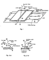
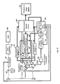
- a moving table 10 which is mounted on sliding bearings 12 secured to an optical bench 14.
- the moving table supports a photoreceptor plate l6 which may be made of any suitable material such as selenium coated onto an aluminum substrate l7.
- a sensor electrode or probe 18 is mounted over the photoreceptor plate on a supporting structure 20 secured to the optical bench 14.
- the sensor electrode or probe shown in Figure 1 is a metal strip having a longitudinal slit therein of a sufficient width to allow the passage of a laser beam 22 which is scanned across the plate through the slit in the electrode.
- the table 10 is moved on sliding bearings 12 using any suitable drive capable of advancing the photoreceptor plate step by step transversely of the laser beam scanning direction.
- an electrostatically charged photoreceptor plate which has been exposed to X-ray radiations to form a latent X-ray image of an object on the photoreceptor surface, is placed on the moving table and is scanned transversely by a pulsed laser beam 22.
- the laser beam causes the photoreceptor charge for each pixel to be neutralized and a signal corresponding to its magnitude is induced in the sensor electrode 18.
- this signal is fed to a preamplifier 24 which is connected to an external measuring circuit to be disclosed later.
- a full scan across the photoreceptor plate has been completed pixel-by-pixel, the photoreceptor plate is moved longitudinally by one pixel diameter and a new transverse scan is made.
- the photoreceptor plate could be fixed and the sensor electrode movable.
- a scanning system has also been envisaged where the photoreceptor plate is continuously moving (as opposed to step by step) with respect to the sensor electrode, during the laser scanning speed has to be adjusted in concert with the laser pixel size and the width of the plate so as to produce contiguous scans across the plate.
- the image resolution (defined by the MTF) of the system in accordance with the present invention is almost independent of the above geometrical factors.
- the width of the probe, in the present system has to be large enough with regard to the laser beam dimension in order to achieve good capacitive coupling with the region around the area to be discharged by the laser.
- the advantage of having a relatively large probe, instead of a narrow probe of about the pixel size of the laser beam, is that the charge induced in the probe in the particular area to be discharged by the laser beam is linearly proportional to the surface charge of the selenium plate. In this situation, the horizontal component of the electric field created by a high spatial modulation of surface charge or a discharged area is averaged to zero. Thus, in such a configuration, the MTF of the system is only limited by the laser spot size and the spatial sampling rate.
- the width of the sensor electrode should be more than two times the size of the laser beam. There is no advantage however in increasing the width of the sensor electrode to more than 30 mm as it would unduly increase the capaticance across the read-out device.
- the amount of charge still coupled to the conductive substrate of the selenium x-ray detector decreases as: Under the action of a pulse of light of short duration compared to the transit time of charges across the selenium thickness of the selenium plate, those neutralized charges which are free to move are only those coupled to the substrate. Thus, one would expect the signal flowing to the probe to increase at closer probe to selenium separations, due to the benefit of a better capacitive coupling.
- Fig 3 shows the agreement between the expected theoretical and experimental measured signal induced in the probe as a function of the ratio of the air gap capacitance between the probe and the selenium plate to the selenium capacitance for two different selenium thicknesses.
- the probe to surface of selenium separation has to be such as to prevent self discharge of the photoreceptor charge onto the probe.
- a dielectric liquid or gas may be used to overcome field breakdown problems.
- the utilization of a dielectric fluid of the same or larger dielectric constant as selenium allows to operate at larger separations while maintaining the same optimum capacitive coupling.
- the microphonic noise due to random vibration of the probe is also reduced by a factor substantially equal to the ratio of the dielectric constant to air.
- a slit-electrode having a width of 25 mm and positioned about 1 mm for the surface of a 150 um thick selenium plate was able to provide a sufficient signal to enable a good reproduction of the latent image on the selenium photoreceptor plate to be obtained. This image could be accurately reproduced even when the image was strongly modulated in the direction of travel of the slit-electrode.
- FIGs 4(a) and 4(b) are examples of one such improved structure, which is representative, but not restrictive as to the nature of the features which can be incorporated into the probe structure in order to improve its operation.
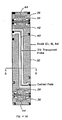
- the read-out probe shown in Figures 4(a) and 4(b) is a solid state device prepared by photolithographic processes on a common semi-cylindrical glass lens substrate. In order to achieve accurate alignment and positioning of the sensor electrode or probe over the photoreceptor plate, several components have been integrated to the probe.
- the read-out probe is thus composed of four components: a transparent sensor electrode designated generally by reference numral 32, an electromagnetic interference shield 34, laser alignment components 36 and capacitance structures 38 for probe micropositioning.
- a transparent sensor electrode designated generally by reference numral 32
- an electromagnetic interference shield 34 laser alignment components 36
- capacitance structures 38 for probe micropositioning.
- the number of devices integrated to the sensor electrode is not necessarily limited to these four.
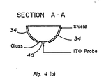
- the transpatent sensor electrode 32 consists of a sputteredum tin oxide (ITO) transparent conductive layer 40, centered with respect to a semi-cylindrical glass lens 42.
- the layer has a typical sheet resistance of 30 ohms/square and over 75% transmission for the visible spectrum.
- the width of the probe has been chosen in order to optimize the characteristic performance of the read-out system. As mentioned previously, a very narrow probe of about the pixel size of the laser would be desirable in order to reduce the microphonic noise associated with the random vibration of the probe with respect to the plate. However, a very narrow probe has a substantial limitation in terms of image resolution. A probe dimension of 1 mm in width has proven to be very satisfactory.
- the transparent sensor electrode is shielded from external electromagnetic interference by a nickel, chromium and gold multilayer shield 34 that effectively surrounds it.
- each slit 44 transversing, at a 45 degree angle, an opaque rectangle at the top of the probe.
- the centre of each slit coincides (lengthwise) with the central axis of the transparent electrode.
- a photodiode detector 46 is placed behind each of the slits 44 and the detector output is connected to an oscilloscope 47.
- the scanning laser beam is then shone along the axis of the probe.
- the probe structure is positioned in such a way that the time the laser beam is obscured from the top edge of each rectangle to the centre of each slit (T1 and T3) and the time the beam is obscured from the centre of each slit to the bottom edge of each rectangle (T2 and T4) are equal.
- T1 and T3 the time the laser beam is obscured from the centre of each slit to the bottom edge of each rectangle
- Figure 5(d) shows the inverse light intensity diagram seen on the oscilloscope when the laser beam is offset and Figure 5(e) the inverse light intensity diagram when the laser beam is centered. When all the times are equal, the laser beam is centrally traversing the transparent probe.
- capacitance structures 38 at the top and bottom of the probe. These structures consist of flat conducting pads. When the probe is positioned near the photoreceptor plate to be read out, a capacitance is formed between the pads and the plate. The capacitance of the pads with respect to selenium surface of the plates is inversely proportional to the separation of the pads from the plate.
- the capacitance of the top and bottom structures are very precisely measured using conventional bridge-type capacitane meters 48.
- the capacitance is measured directly whilst a phase signal from the bridge indicates whether or not the probe/plate separation is greater or less than a predetermined separation.
- the output of each capacitance meter is fed to a microprocessor system control 50.
- piezoelectric micropositioners 52 one at both the top and bottom of the probe structure
- a piezoelectric positioner controller 54 which is responsive to microprocessor 50, it is possible to precisely move the probe in such a way that the capacitance structures are equal.
- the probe/plate separation is constant from top to bottom of the probe. This is essential for maintaining signal uniformity along a scan.
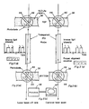
- the selenium plate scanning system consists of a conventional optical assembly and a conventional processing and digital control.
- a galvanometer 56 is used to scan a blue laser beam (440 nm) through a F-Theta lens 58 and onto the selenium plate 16.
- the laser beam itself is generated by a laser 60 and modulated into properly timed pulses by the use of an acousto-optic modulator 62 responsive to a programmable high speed scan control 64 under the control of microprocessor 50.
- the laser itself is stabilized by an electro-optic stabilizer 66.
- the laser beam passes through a neutral density filter 68 and is deflected by mirrors 70 onto galvanometer 56.
- a translation stage controller 72 is provided for moving the photoreceptor support table 10 transversely to the scanning laser beam at the end of each scan.
- the translation stage controller is under the control of the microprocessor system control.
- the analog signal at the output of the preamplifier 24 is then processed through an analog processing unit 74 and digitized by an A/D converter 75 and stored in digital form in microprocessor 50 and can be viewed and disseminated at command using a processor and image display 76.
- the synchronization and coordination of scanning activities plus data storage may be managed by a Motorola 68000 microprocessor system and associated real-time scan logic. The details and timing of the scan process and data acquisition need not be discussed here.
- the overall results are very encouraging.
- MTF modulation transfer function
- the MTFs shown in Figure 7 are for a selenium coated plate with a selenium thickness of l50um, measured with a lmm wide transparent conductive ITO electrode on glass.
- the MTF curves are for two different laser spot sizes and spatial sampling rates. For a l00 um laser spot diameter and 10 samples/mm, a resolution of 5 1p/mm has been easily attained. Also, as expected from theory, by increasing the sampling rate to 20 samples/mm and using a 50 um laser spot size a resolution of 10 1p/mm has been achieved.
Landscapes
- Physics & Mathematics (AREA)
- General Physics & Mathematics (AREA)
- Engineering & Computer Science (AREA)
- Multimedia (AREA)
- Signal Processing (AREA)
- Measurement Of Radiation (AREA)
- Transforming Light Signals Into Electric Signals (AREA)
Applications Claiming Priority (2)
| Application Number | Priority Date | Filing Date | Title |
|---|---|---|---|
| CA553214 | 1987-12-01 | ||
| CA000553214A CA1276320C (fr) | 1987-12-01 | 1987-12-01 | Systeme pour mesurer la repartition de la charge en surface d'un photorecepteur |
Publications (2)
| Publication Number | Publication Date |
|---|---|
| EP0318807A1 true EP0318807A1 (fr) | 1989-06-07 |
| EP0318807B1 EP0318807B1 (fr) | 1994-02-23 |
Family
ID=4136979
Family Applications (1)
| Application Number | Title | Priority Date | Filing Date |
|---|---|---|---|
| EP88119432A Expired - Lifetime EP0318807B1 (fr) | 1987-12-01 | 1988-11-22 | Système de mesure de distribution de charge sur une surface photoréceptrice |
Country Status (5)
| Country | Link |
|---|---|
| US (1) | US4961209A (fr) |
| EP (1) | EP0318807B1 (fr) |
| CA (1) | CA1276320C (fr) |
| DE (1) | DE3887968T2 (fr) |
| ES (1) | ES2050141T3 (fr) |
Cited By (4)
| Publication number | Priority date | Publication date | Assignee | Title |
|---|---|---|---|---|
| EP0573199A3 (fr) * | 1992-06-01 | 1994-02-23 | Xerox Corp | |
| WO1994004963A1 (fr) * | 1992-08-14 | 1994-03-03 | E.I. Du Pont De Nemours And Company | Element, dispositif et procede associe de prise d'une image radiographique latente |
| WO1994017423A1 (fr) * | 1993-01-29 | 1994-08-04 | Minnesota Mining And Manufacturing Company | Systeme et procede assurant l'ecartement uniforme d'une electrode sur la surface d'une plaque a rayons x |
| EP0798018A3 (fr) * | 1996-03-29 | 2000-11-15 | McGILL UNIVERSITY | Imagerie mégatension utilisant la combinaison d'un photorécepteur et d'un convertisseur, intensificateur de photons de grande énergie |
Families Citing this family (30)
| Publication number | Priority date | Publication date | Assignee | Title |
|---|---|---|---|---|
| US5168160A (en) * | 1991-06-28 | 1992-12-01 | E. I. Du Pont De Nemours And Company | Method and apparatus for acquiring an electrical signal representing a radiographic image |
| US5127038A (en) * | 1991-06-28 | 1992-06-30 | E. I. Du Pont De Nemours And Company | Method for capturing and displaying a latent radiographic image |
| US5166524A (en) * | 1991-06-28 | 1992-11-24 | E. I. Du Pont De Nemours & Company | Element, device and associated method for capturing a latent radiographic image |
| US5331179A (en) * | 1993-04-07 | 1994-07-19 | E. I. Du Pont De Nemours And Company | Method and apparatus for acquiring an X-ray image using a thin film transistor array |
| US5313066A (en) * | 1992-05-20 | 1994-05-17 | E. I. Du Pont De Nemours And Company | Electronic method and apparatus for acquiring an X-ray image |
| US5268569A (en) * | 1992-07-22 | 1993-12-07 | Minnesota Mining And Manufacturing Company | Imaging system having optimized electrode geometry and processing |
| US5332893A (en) * | 1992-07-22 | 1994-07-26 | Minnesota Mining And Manufacturing Company | Imaging system and device having a simplified electrode design |
| US5319206A (en) * | 1992-12-16 | 1994-06-07 | E. I. Du Pont De Nemours And Company | Method and apparatus for acquiring an X-ray image using a solid state device |
| US5661309A (en) * | 1992-12-23 | 1997-08-26 | Sterling Diagnostic Imaging, Inc. | Electronic cassette for recording X-ray images |
| US5311033A (en) * | 1993-04-01 | 1994-05-10 | Minnesota Mining And Manufacturing Company | Layered imaging stack for minimizing interference fringes in an imaging device |
| US5381014B1 (en) * | 1993-12-29 | 1997-06-10 | Du Pont | Large area x-ray imager and method of fabrication |
| EP0753232A1 (fr) * | 1994-03-31 | 1997-01-15 | Imation Corp. | Systeme d'imagerie mettant en uvre des electrodes a geometrie variable, et traitement |
| US5440146A (en) * | 1994-03-31 | 1995-08-08 | Minnesota Mining And Manufacturing Company | Radiographic image reader |
| US5498880A (en) * | 1995-01-12 | 1996-03-12 | E. I. Du Pont De Nemours And Company | Image capture panel using a solid state device |
| FR2751095B1 (fr) * | 1996-07-09 | 1998-10-30 | Thomson Csf | Dispositif de controle d'impulsions lumineuses par un dispositif programmable acousto-optique |
| US5994713A (en) * | 1997-06-25 | 1999-11-30 | Quantum Imaging Corp. | Filmless photon imaging apparatus |
| EP0898421A3 (fr) | 1997-08-19 | 2001-12-05 | Fuji Photo Film Co., Ltd. | Elément d'enregistrement électrostatique, appareil d'enregistrement/reproduction d'images électrostatiques latentes |
| IL123006A (en) | 1998-01-20 | 2005-12-18 | Edge Medical Devices Ltd | X-ray imaging system |
| JP2000029612A (ja) * | 1998-07-15 | 2000-01-28 | Smk Corp | タッチパネル入力装置 |
| IL126018A0 (en) | 1998-09-01 | 1999-05-09 | Edge Medical Devices Ltd | X-ray imaging system |
| US6326625B1 (en) | 1999-01-20 | 2001-12-04 | Edge Medical Devices Ltd. | X-ray imaging system |
| US6178225B1 (en) | 1999-06-04 | 2001-01-23 | Edge Medical Devices Ltd. | System and method for management of X-ray imaging facilities |
| US6717173B2 (en) * | 2000-02-08 | 2004-04-06 | Fuji Photo Film Co., Ltd. | Radio-conductive material, method of manufacturing the same, solid sensor using the same, method of manufacturing radio-conductive film, and radiation image read-out apparatus |
| US6195272B1 (en) | 2000-03-16 | 2001-02-27 | Joseph E. Pascente | Pulsed high voltage power supply radiography system having a one to one correspondence between low voltage input pulses and high voltage output pulses |
| JP2001264442A (ja) | 2000-03-22 | 2001-09-26 | Fuji Photo Film Co Ltd | 画像記録媒体 |
| US6590224B2 (en) | 2000-03-22 | 2003-07-08 | Fuji Photo Film Co., Ltd. | Image storage medium and method of manufacturing the same |
| US6774385B2 (en) | 2000-03-22 | 2004-08-10 | Fuji Photo Film Co., Ltd. | Image recording medium and method of manufacturing the same |
| JP2001281345A (ja) | 2000-03-31 | 2001-10-10 | Fuji Photo Film Co Ltd | エネルギー線検出装置およびその温度調整方法 |
| JP4361538B2 (ja) * | 2006-02-16 | 2009-11-11 | 株式会社フューチャービジョン | ガラス基板の除電方法 |
| JP6989852B2 (ja) * | 2019-01-22 | 2022-02-03 | 横河電機株式会社 | 電界センサ |
Citations (3)
| Publication number | Priority date | Publication date | Assignee | Title |
|---|---|---|---|---|
| EP0020030A1 (fr) * | 1979-05-11 | 1980-12-10 | Vacuumatic Limited | Unité de pesage |
| CA1155562A (fr) * | 1981-02-11 | 1983-10-18 | Ronald W. Cowart | Appareil de surveillance et de controle en temps reel de l'exposition aux radiations |
| EP0219897A1 (fr) * | 1985-09-30 | 1987-04-29 | Philips Patentverwaltung GmbH | Dispositif d'acquisition d'image rayons X par photoconducteur |
Family Cites Families (3)
| Publication number | Priority date | Publication date | Assignee | Title |
|---|---|---|---|---|
| US4085327A (en) * | 1977-01-14 | 1978-04-18 | General Electric Company | Direct charge readout electron radiography apparatus with improved signal-to-noise ratio |
| US4204725A (en) * | 1977-11-17 | 1980-05-27 | International Business Machines Corporation | Apparatus for detecting information stored on photocopying media, transmitting and storing the same |
| US4663526A (en) * | 1984-12-26 | 1987-05-05 | Emil Kamieniecki | Nondestructive readout of a latent electrostatic image formed on an insulating material |
-
1987
- 1987-12-01 CA CA000553214A patent/CA1276320C/fr not_active Expired - Lifetime
-
1988
- 1988-11-22 ES ES88119432T patent/ES2050141T3/es not_active Expired - Lifetime
- 1988-11-22 EP EP88119432A patent/EP0318807B1/fr not_active Expired - Lifetime
- 1988-11-22 DE DE3887968T patent/DE3887968T2/de not_active Expired - Fee Related
- 1988-11-30 US US07/278,274 patent/US4961209A/en not_active Expired - Fee Related
Patent Citations (3)
| Publication number | Priority date | Publication date | Assignee | Title |
|---|---|---|---|---|
| EP0020030A1 (fr) * | 1979-05-11 | 1980-12-10 | Vacuumatic Limited | Unité de pesage |
| CA1155562A (fr) * | 1981-02-11 | 1983-10-18 | Ronald W. Cowart | Appareil de surveillance et de controle en temps reel de l'exposition aux radiations |
| EP0219897A1 (fr) * | 1985-09-30 | 1987-04-29 | Philips Patentverwaltung GmbH | Dispositif d'acquisition d'image rayons X par photoconducteur |
Cited By (4)
| Publication number | Priority date | Publication date | Assignee | Title |
|---|---|---|---|---|
| EP0573199A3 (fr) * | 1992-06-01 | 1994-02-23 | Xerox Corp | |
| WO1994004963A1 (fr) * | 1992-08-14 | 1994-03-03 | E.I. Du Pont De Nemours And Company | Element, dispositif et procede associe de prise d'une image radiographique latente |
| WO1994017423A1 (fr) * | 1993-01-29 | 1994-08-04 | Minnesota Mining And Manufacturing Company | Systeme et procede assurant l'ecartement uniforme d'une electrode sur la surface d'une plaque a rayons x |
| EP0798018A3 (fr) * | 1996-03-29 | 2000-11-15 | McGILL UNIVERSITY | Imagerie mégatension utilisant la combinaison d'un photorécepteur et d'un convertisseur, intensificateur de photons de grande énergie |
Also Published As
| Publication number | Publication date |
|---|---|
| DE3887968T2 (de) | 1994-10-06 |
| CA1276320C (fr) | 1990-11-13 |
| EP0318807B1 (fr) | 1994-02-23 |
| DE3887968D1 (de) | 1994-03-31 |
| US4961209A (en) | 1990-10-02 |
| ES2050141T3 (es) | 1994-05-16 |
Similar Documents
| Publication | Publication Date | Title |
|---|---|---|
| EP0318807B1 (fr) | Système de mesure de distribution de charge sur une surface photoréceptrice | |
| EP0002102B1 (fr) | Dispositif de reproduction / d'impression xérographique avec conversion de l'information d'une image latente d'un original en signaux electriques | |
| US4816863A (en) | Exposure control system for continuous tone electrophotographic film | |
| US6008653A (en) | Contactless system for detecting microdefects on electrostatographic members | |
| US5268569A (en) | Imaging system having optimized electrode geometry and processing | |
| US4134137A (en) | Single wire microelectrometer imaging system | |
| JPS6252981B2 (fr) | ||
| CA2288261C (fr) | Appareil d'imagerie photonique sans film | |
| US5168160A (en) | Method and apparatus for acquiring an electrical signal representing a radiographic image | |
| JPH05210287A (ja) | 電子写真画像形成におけるコントラスト強調方法及び装置 | |
| US5508507A (en) | Imaging system employing effective electrode geometry and processing | |
| US3752572A (en) | Apparatus for making electrographs | |
| EP0573199A2 (fr) | Elément de reproduction d'images à rayons X, à base d'un alliage de sélénium déposé sur un substrat transparant | |
| US5332893A (en) | Imaging system and device having a simplified electrode design | |
| US4296478A (en) | Readout of electrostatically stored information | |
| KR20010090708A (ko) | 시간상수가 조정된 유전층을 구비한 직동식 방사선 투과사진용 영상 패널 | |
| US4636069A (en) | Method for reading deformation images on electrophotographic media | |
| Yarmchuk et al. | High‐resolution surface charge measurements on an organic photoconductor | |
| US3638110A (en) | Device for measuring charge on a material by converting into electrical signals the frictional forces caused by the charge | |
| US7271593B2 (en) | Contactless system and method for detecting defective points on a chargeable surface | |
| JPH02143778A (ja) | 電荷潜像の読取り方式 | |
| US6756603B2 (en) | Imaging apparatus | |
| US3742374A (en) | Transducer device | |
| US6737667B1 (en) | Image recording medium, image retrieving method and image retrieving apparatus | |
| US20020150203A1 (en) | X-ray image converter, device and method for recording, processing and illustrating images using X-rays and other rays |
Legal Events
| Date | Code | Title | Description |
|---|---|---|---|
| PUAI | Public reference made under article 153(3) epc to a published international application that has entered the european phase |
Free format text: ORIGINAL CODE: 0009012 |
|
| AK | Designated contracting states |
Kind code of ref document: A1 Designated state(s): BE CH DE ES FR GB IT LI NL SE |
|
| 17P | Request for examination filed |
Effective date: 19891027 |
|
| 17Q | First examination report despatched |
Effective date: 19920128 |
|
| RAP1 | Party data changed (applicant data changed or rights of an application transferred) |
Owner name: NORANDA INC. |
|
| GRAA | (expected) grant |
Free format text: ORIGINAL CODE: 0009210 |
|
| AK | Designated contracting states |
Kind code of ref document: B1 Designated state(s): BE CH DE ES FR GB IT LI NL SE |
|
| PG25 | Lapsed in a contracting state [announced via postgrant information from national office to epo] |
Ref country code: SE Effective date: 19940223 Ref country code: LI Effective date: 19940223 Ref country code: CH Effective date: 19940223 |
|
| REF | Corresponds to: |
Ref document number: 3887968 Country of ref document: DE Date of ref document: 19940331 |
|
| REG | Reference to a national code |
Ref country code: ES Ref legal event code: FG2A Ref document number: 2050141 Country of ref document: ES Kind code of ref document: T3 |
|
| ITF | It: translation for a ep patent filed | ||
| REG | Reference to a national code |
Ref country code: CH Ref legal event code: PL |
|
| ET | Fr: translation filed | ||
| PLBE | No opposition filed within time limit |
Free format text: ORIGINAL CODE: 0009261 |
|
| STAA | Information on the status of an ep patent application or granted ep patent |
Free format text: STATUS: NO OPPOSITION FILED WITHIN TIME LIMIT |
|
| 26N | No opposition filed | ||
| PGFP | Annual fee paid to national office [announced via postgrant information from national office to epo] |
Ref country code: BE Payment date: 19961031 Year of fee payment: 9 |
|
| PGFP | Annual fee paid to national office [announced via postgrant information from national office to epo] |
Ref country code: ES Payment date: 19961107 Year of fee payment: 9 |
|
| PGFP | Annual fee paid to national office [announced via postgrant information from national office to epo] |
Ref country code: GB Payment date: 19961113 Year of fee payment: 9 |
|
| PGFP | Annual fee paid to national office [announced via postgrant information from national office to epo] |
Ref country code: FR Payment date: 19961126 Year of fee payment: 9 |
|
| PGFP | Annual fee paid to national office [announced via postgrant information from national office to epo] |
Ref country code: NL Payment date: 19961129 Year of fee payment: 9 |
|
| PGFP | Annual fee paid to national office [announced via postgrant information from national office to epo] |
Ref country code: DE Payment date: 19970130 Year of fee payment: 9 |
|
| PG25 | Lapsed in a contracting state [announced via postgrant information from national office to epo] |
Ref country code: GB Free format text: LAPSE BECAUSE OF NON-PAYMENT OF DUE FEES Effective date: 19971122 |
|
| PG25 | Lapsed in a contracting state [announced via postgrant information from national office to epo] |
Ref country code: ES Free format text: LAPSE BECAUSE OF NON-PAYMENT OF DUE FEES Effective date: 19971123 |
|
| PG25 | Lapsed in a contracting state [announced via postgrant information from national office to epo] |
Ref country code: FR Free format text: THE PATENT HAS BEEN ANNULLED BY A DECISION OF A NATIONAL AUTHORITY Effective date: 19971130 Ref country code: BE Free format text: LAPSE BECAUSE OF NON-PAYMENT OF DUE FEES Effective date: 19971130 |
|
| BERE | Be: lapsed |
Owner name: NORANDA INC. Effective date: 19971130 |
|
| PG25 | Lapsed in a contracting state [announced via postgrant information from national office to epo] |
Ref country code: NL Free format text: LAPSE BECAUSE OF NON-PAYMENT OF DUE FEES Effective date: 19980601 |
|
| GBPC | Gb: european patent ceased through non-payment of renewal fee |
Effective date: 19971122 |
|
| PG25 | Lapsed in a contracting state [announced via postgrant information from national office to epo] |
Ref country code: DE Free format text: LAPSE BECAUSE OF NON-PAYMENT OF DUE FEES Effective date: 19980801 |
|
| NLV4 | Nl: lapsed or anulled due to non-payment of the annual fee |
Effective date: 19980601 |
|
| REG | Reference to a national code |
Ref country code: FR Ref legal event code: ST |
|
| REG | Reference to a national code |
Ref country code: ES Ref legal event code: FD2A Effective date: 19981212 |
|
| PG25 | Lapsed in a contracting state [announced via postgrant information from national office to epo] |
Ref country code: IT Free format text: LAPSE BECAUSE OF NON-PAYMENT OF DUE FEES;WARNING: LAPSES OF ITALIAN PATENTS WITH EFFECTIVE DATE BEFORE 2007 MAY HAVE OCCURRED AT ANY TIME BEFORE 2007. THE CORRECT EFFECTIVE DATE MAY BE DIFFERENT FROM THE ONE RECORDED. Effective date: 20051122 |