EP0319063A2 - Spannungsvervielfacher und Gleichrichterelement - Google Patents
Spannungsvervielfacher und Gleichrichterelement Download PDFInfo
- Publication number
- EP0319063A2 EP0319063A2 EP88202531A EP88202531A EP0319063A2 EP 0319063 A2 EP0319063 A2 EP 0319063A2 EP 88202531 A EP88202531 A EP 88202531A EP 88202531 A EP88202531 A EP 88202531A EP 0319063 A2 EP0319063 A2 EP 0319063A2
- Authority
- EP
- European Patent Office
- Prior art keywords
- field effect
- effect transistor
- multiplier circuit
- voltage multiplier
- voltage
- Prior art date
- Legal status (The legal status is an assumption and is not a legal conclusion. Google has not performed a legal analysis and makes no representation as to the accuracy of the status listed.)
- Granted
Links
Images
Classifications
-
- H—ELECTRICITY
- H03—ELECTRONIC CIRCUITRY
- H03K—PULSE TECHNIQUE
- H03K17/00—Electronic switching or gating, i.e. not by contact-making and –breaking
-
- H—ELECTRICITY
- H02—GENERATION; CONVERSION OR DISTRIBUTION OF ELECTRIC POWER
- H02M—APPARATUS FOR CONVERSION BETWEEN AC AND AC, BETWEEN AC AND DC, OR BETWEEN DC AND DC, AND FOR USE WITH MAINS OR SIMILAR POWER SUPPLY SYSTEMS; CONVERSION OF DC OR AC INPUT POWER INTO SURGE OUTPUT POWER; CONTROL OR REGULATION THEREOF
- H02M3/00—Conversion of DC power input into DC power output
- H02M3/02—Conversion of DC power input into DC power output without intermediate conversion into AC
- H02M3/04—Conversion of DC power input into DC power output without intermediate conversion into AC by static converters
- H02M3/06—Conversion of DC power input into DC power output without intermediate conversion into AC by static converters using resistors or capacitors, e.g. potential divider
- H02M3/07—Conversion of DC power input into DC power output without intermediate conversion into AC by static converters using resistors or capacitors, e.g. potential divider using capacitors charged and discharged alternately by semiconductor devices with control electrode, e.g. charge pumps
- H02M3/073—Charge pumps of the Schenkel-type
-
- G—PHYSICS
- G11—INFORMATION STORAGE
- G11C—STATIC STORES
- G11C5/00—Details of stores covered by group G11C11/00
- G11C5/14—Power supply arrangements, e.g. power down, chip selection or deselection, layout of wirings or power grids, or multiple supply levels
- G11C5/145—Applications of charge pumps; Boosted voltage circuits; Clamp circuits therefor
Definitions
- the invention relates to an integrated voltage multiplier circuit, comprising a high-voltage output connected to a series connection of rectifier elements, each of which comprises a first field effect transistor, a buffer capacitance for charge storage being connected between the high-voltage output and a power supply terminal, a junction point of every pair of neighbouring elements being connected to one side of a booster capacitance whereto clock signals are applied on the other side so that two booster capacitances connected to a respective side of one rectifier element receive clock signals of mutually opposed polarity.
- the invention also relates to a rectifier element suitable for use in such a voltage multiplier circuit.
- Voltage multiplier circuits of this kind are known, for example from IEEE Solid State Circuits, SC-11(3), June 1976, page 375, and are used inter alia in non-volatile electrically programmable and erasable memories.
- a conventional voltage multiplier circuit for generating a negative output voltage comprises a series connection of PMOS transistors which are connected as diodes and which are realized in a P-well proces, said series connection being connected at a cathode side to a point carrying a low supply voltage V SS (ground) and comprising at an anode side an output with a buffer capacitance for supplying a high programming voltage.
- the buffer capacitance is connected between the output and a high supply voltage V DD .
- the substrate in which these transistors are embedded is of the N-type and, in order to avoid the injection of charge carriers from the transistors to the substrate, it is coupled to the high supply voltage (V DD ).
- a junction point of each pair of neighbouring diodes is connected, via a respective booster capacitance, to either a first clock line or a second clock line, which clock lines carry logically complementary clock signals.
- the various booster capacitances alternately receive clock signals of opposed sign. Because the sign of the clock signals periodically changes, the diodes are alternately conductive and blocked and charge is transferred from one booster capacitance to the other via a conductive diode.
- the level of the output voltage of the voltage multiplier circuit is limited by this effect.
- the transfer of charge from the buffer capacitance, via the diode, to the next booster capacitance stops when the voltage swing between the clock lines is too small to raise the voltage on the anode of the diode one threshold voltage beyond the voltage on the cathode of the diode. In order to obtain a higher negative output voltage, a larger voltage swing and hence a higher supply voltage would be required.
- a voltage multiplier circuit in accordance with the invention is characterized in that the field effect transistors of the elements on a substrate are realized in separate regions of a conductivity type other than that of the substrate, at least the rectifier elements which are situated at a high-voltage side of the circuit comprising respective switching means which connect internal diodes, formed in the field effect transistor by a p-n junctions between a source and a drain, respectively, of the field effect transistor on the one side and the region on the other side, to either the source in the conductive state or to the drain in the blocked state of the field effect transistor, so that the internal diodes remain blocked.
- the back-gate bias voltage remains zero.
- the parasitic bipolar transistor whose collector, base and emitter are formed by the substrate, the well and the drain, respectively, will not become conductive.
- An embodiment of a voltage multiplier circuit in accordance with the invention is characterized in that the switching means of the first field effect transistor comprise a second and a third field effect transistor which are of the same conductivity type as the first field effect transistor and which are realized in respective regions which are coupled to the region of the first field effect transistor, a source of the second and the third field effect transistor being connected to a source and a drain, respectively, of the first field effect transistor, a control electrode of the second and the third field effect transistor being coupled to the drain and the source, respectively, of the first field effect transistor, the drains of the second and the third transistor being connected to the interconnected regions.
- the switching means in the form of a second and third transistor have a compact construction and need not be driven by additional control signals. Such a construction comprising NMOS transistors in a P-well is suitable for generating high negative voltages.
- a voltage multiplier constructed by means of PMOS transistors is suitable for generating high positive voltages.
- a further embodiment of a voltage multiplier circuit in accordance with the invention is characterized in that the voltage multiplier circuit comprises a multi-phase clock signal generator for applying respective, mutually phase-shifted clock signals to respective booster capacitances, the clock signal applied to the source of the first field effect transistor via the relevant booster capacitance changing sooner than the complementary clock signal applied to the drain of the first field effect transistor via the next booster capacitance.
- the voltage multiplier circuit comprises a multi-phase clock signal generator for applying respective, mutually phase-shifted clock signals to respective booster capacitances, the clock signal applied to the source of the first field effect transistor via the relevant booster capacitance changing sooner than the complementary clock signal applied to the drain of the first field effect transistor via the next booster capacitance.
- the bipolar parasitic transistor When the voltage on the source is made to rise or decrease before the voltage on the drain of the first transistor decreases or increases, respectively, by applying phase-shifted, complementary clock signals to said main electrodes via the relevant booster capacitances, the bipolar parasitic transistor whose collector, base and emitter are formed by the substrate, the well and the source of the first transistor, respectively, will not become conductive.
- a further embodiment of a voltage multiplier circuit in accordance with the invention is characterized in that the multi-phase clock signal generator comprises a series connection of a number of inverter circuits, respective outputs of two neighbouring inverter circuits being connected to respective electrodes of two neighbouring booster capacitances.
- the clock signal generator then comprises a series connection of inverter circuits for applying clock signals to the neighbouring booster capacitances in phase opposition, a gate delay of an inverter circuit causing the above-mentioned phase shift.
- a preferred embodiment of a voltage multiplier circuit in accordance with the invention is characterized in that in the element between a connection point of the control electrode of the first and the second field effect transistor on the one side and the drain of the first field effect transistor on the other side there is provided a switchable charging or discharging path for charging or discharging the latter control electrodes, there being provided control means which are connected to the latter connection point via a coupling capacitance in order to increase or decrease a voltage on the latter control electrodes after they have been charged or discharged, respectively, via the switchable charging or discharging path.
- the voltage across the first field effect transistor is thus reduced to substantially zero in the forward direction because no threshold loss occurs. This threshold loss is avoided by adding to the control voltage already present on the control electrode of the first transistor, via the coupling capacitance, a control voltage originating from the control means.
- a voltage multiplier circuit in accordance with the invention in which the series connection of inverter circuits forms a part of a ring oscillator, is characterized in that the ring oscillator comprises a flipflop, a flipflop output of which is fed back, via the inverters, to a first flipflop input, a second flipflop input receiving an enable signal. Because a flipflop is included in the ring oscillator, the ring oscillator can be switched off after a complete last clock pulse.
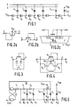
- Fig. 1 shows a conventional voltage multiplier circuit of the type generating a negative output voltage.
- a series connection of rectifier elements D1, D2, ... D n Between the output V EE and the power supply terminal V DD there is connected a buffer capacitance C EE .
- the respective junctions K1, K2, ..., K n-1 are alternately connected, via an associated booster capacitance C1, C2, ..., C n-1, to clock lines Q and Q which carry complementary clock signals.
- the rectifier elements having an even index, D2, D4, ..., and the elements having an odd index, D1, D3, ..., will periodically be blocked or conductive and conductive or blocked, respectively.
- Charge is then pumped, via a conductive element, from one booster capacitance to the next booster capacitance having a lower index. Charge is thus step-wise fetched from the buffer capacitance C EE and ultimately drained on the V SS terminal.
- Figs. 2a and b show conventional rectifier elements for a voltage multiplier circuit as shown in Fig. 1 which is constructed by means of field effect transistors.
- the element shown in Fig. 2a is a PMOS transistor which is connected as a diode and a substrate connection SU of which is connected to the positive supply terminal V DD in order to avoid charge injection to the substrate.
- the threshold voltage at which the element becomes conductive is also higher. This is because the threshold voltage increases as the substrate-source voltage increases.
- the threshold voltage of the rectifier element becomes so high that the voltage swing on the clock lines Q and Q is no longer sufficient to raise the voltage difference across the element D n in the forward direction beyond the threshold voltage of the transistor.
- the element shown in the Figs. 2b and 2c is an NMOS transistor which is connected as a diode and which is realized in a P-well.
- the well connection W is connected to the anode A in order to prevent charge injection to the well. If the voltage on the side of the cathode K is lower than that on the anode side, a parasitic bipolar transistor PB is set to the conductive state.
- Fig. 3 shows a circuit diagram of a rectifier element in accordance with the invention.
- the invention is based on the recognition of the fact that the element shown in the Figs. 2b and 2c is suitable as a rectifier element for the voltage multiplier circuit shown in Fig. 1 only if the voltage on the cathode terminal K cannot drop below that of the well and hence below that on the anode terminal A, so that the parasitic transistor PB becomes conductive. If the well connection according to the invention is always switched to the main electrode of the NMOS transistor which carries the lowest voltage, the problem described with reference to Fig. 2c is solved. This is shown in Fig. 3.
- the diodes between the N diffusions for the main electrodes on the one side and the P-well on the other side are connected, depending on the voltage on the cathode K and the anode A, to either the cathode terminal K or to the anode terminal A, so that the diodes are always blocked.
- Fig. 4 shows a first embodiment of a rectifier element for a voltage multiplier circuit in accordance with the invention.
- a P-well terminal W of a first NMOS transistor N1 which is connected as a diode is coupled to the cathode K of the transistor N1 across a second transistor N2 and to the anode A of the transistor N1 across a third transistor N3.
- the coupling of the control electrodes of the transistor N2 and of the transistor N3 to the anode A and the cathode K, respectively, of the transistor N1 ensures that the P-well is always connected to the lowest voltage occurring on one of the main electrodes of the transistor N1, except when the voltage across the transistor N1 is lower than a threshold voltage of the transistors N2 and N3.
- the P-well is uncoupled from the anode A as well as from the cathode K.
- the P-well maintains its voltage on the junction capacitance between the P-well and the substrate.
- the voltage on the source of the transistor N1 junction K
- the voltage on the source of the transistor N1 junction K
- the drain junction A
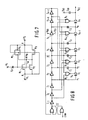
- Fig. 5 shows a first embodiment of a voltage multiplier circuit in accordance with the invention.
- This voltage multiplier circuit generates a negative output voltage V EE .
- the series connection of the rectifier elements of the type described with reference to Fig. 4, R1, R2, ..., R n is connected to a power supply terminal V DD at an anode side, via a buffer capacitance C EE .
- Each of the junctions between two elements is connected, via booster capacitances, to a junction point between two inverters I2, I3, ..., I n .
- the series connection of the inverters forms part of a ring oscillator RT which also includes a flipflop FF.
- the successive booster capacitances C1, C2, ..., C n-1 receive clock signals in phase opposition, as has already been described with reference to. Fig. 1. Moreover, the clock signals applied to the successive booster capacitances are delayed with respect to one another by a time interval which equals one inverter delay.
- This inverter delay ensures that the voltage on the source (for example, the junction V2) of the first transistor in an element (for example, R2) changes before the voltage on the drain (for example, junction point V3) of said first transistor changes.
- this serves to prevent parasitic bipolar transistors from becoming conductive in blocked rectifier elements, thus disturbing the potential built up at said rectifier element.
- Flipflop FF is included in the ring oscillator RT in order to ensure that, when the ring oscillator is switched off by means of the enable signal EVM, the last clock pulse is still fully passed on, resulting in better defined states in the oscillator.
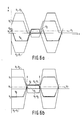
- Fig. 6a shows the variation of the voltages denoted by the references V1 and V2 in Fig. 5 and the references V1, V2 and V B in Fig. 4.
- Fig. 6b shows the variation of these signals if the signals on the source of the first transistor in an element were to change simultaneously with the signals on its drain.
- Signal V1 is the signal on the source of the transistor N1 of Fig. 4 and V2 is the signal on the drain of the transistor N1.
- the signal V2 has a lower mean value than V1 because charge is step-wise drained from the buffer capacitance C EE , having a high negative voltage, across the various stage capacitances C1, C2, ..., C n , to V SS .
- Fig. 7 shows a preferred embodiment of a rectifier element for an integrated voltage multiplier circuit in accordance with the invention. Parts which correspond to those shown in Fig. 4 are denoted by corresponding reference numerals.
- the rectifier transistor N1 and the second transistor N2 are no longer controlled by the forward voltage on the junction point A, as was the case in the circuit shown in Fig. 4.
- the connection between the drain of N1 and the control electrode of N1 is now formed by a current path which can be switched on and off and which comprises a gate transistor N5 which is connected as a diode and a gate transistor N4 which is connected thereto in anti-parallel and which is controlled by a voltage on the junction point K.
- Fig. 8 shows a second embodiment of a voltage multiplier circuit in accordance with the invention. Parts which correspond to those shown in Fig. 5 are denoted by corresponding reference numerals.
- the series connection of rectifier elements G1, G2, ..., G n now comprises rectifier elements of the type shown in Fig. 7.
- Each of these elements G1, G2, ..., G n comprises an additional control input coupled to an associated NOR-gate B1, B2, ..., B n .
- An output of such a NOR-gate supplies the pulse signal V G , described with reference to Fig. 7, on the coupling capacitance C p .
- the operation will be described with reference to the element G1 of Fig. 8 which is explicitly shown in Fig. 7.
- the transistor N4 When the voltage V2 exceeds the voltage V1, the transistor N4 is blocked.
- the NOR-gate B1 initially supplies an output signal equal to V SS .
- the control electrode of the transistor N1 When the voltage V2 increases, the control electrode of the transistor N1 is raised to a higher voltage via the source follower N5.
- the NOR-gate B1 changes over from V DD to V SS , after which the reverse voltage V1 - V2 is built up across the transistor N1.
- the correct phase for driving the elements via the NOR-gate is derived from the voltages on the inputs and outputs of the inverters I ⁇ 1, I0, I1, ..., I n+2 of the ring oscillator.
Landscapes
- Engineering & Computer Science (AREA)
- Power Engineering (AREA)
- Dc-Dc Converters (AREA)
- Semiconductor Integrated Circuits (AREA)
Applications Claiming Priority (2)
| Application Number | Priority Date | Filing Date | Title |
|---|---|---|---|
| NL8702734 | 1987-11-17 | ||
| NL8702734A NL8702734A (nl) | 1987-11-17 | 1987-11-17 | Spanningsvermenigvuldigschakeling en gelijkrichtelement. |
Publications (3)
| Publication Number | Publication Date |
|---|---|
| EP0319063A2 true EP0319063A2 (de) | 1989-06-07 |
| EP0319063A3 EP0319063A3 (en) | 1989-06-21 |
| EP0319063B1 EP0319063B1 (de) | 1992-04-29 |
Family
ID=19850923
Family Applications (1)
| Application Number | Title | Priority Date | Filing Date |
|---|---|---|---|
| EP88202531A Expired - Lifetime EP0319063B1 (de) | 1987-11-17 | 1988-11-14 | Spannungsvervielfacher und Gleichrichterelement |
Country Status (6)
| Country | Link |
|---|---|
| US (1) | US4922403A (de) |
| EP (1) | EP0319063B1 (de) |
| JP (1) | JP2628724B2 (de) |
| KR (1) | KR0136664B1 (de) |
| DE (1) | DE3870592D1 (de) |
| NL (1) | NL8702734A (de) |
Cited By (16)
| Publication number | Priority date | Publication date | Assignee | Title |
|---|---|---|---|---|
| EP0572066A3 (en) * | 1992-05-26 | 1994-06-15 | Philips Patentverwaltung | Circuit to generate a supply voltage |
| EP0678970A3 (de) * | 1994-04-20 | 1998-03-04 | Nippon Steel Corporation | Halbleiter-Spannungserhöhungsschaltung |
| WO1998033264A1 (de) * | 1997-01-24 | 1998-07-30 | Siemens Aktiengesellschaft | Schaltungsanordnung zum erzeugen negativer spannungen |
| FR2759507A1 (fr) * | 1997-02-12 | 1998-08-14 | Sgs Thomson Microelectronics | Pompe de charge dans une technologie a double caisson |
| FR2773012A1 (fr) * | 1997-12-24 | 1999-06-25 | Sgs Thomson Microelectronics | Dispositif a pompe de charges negatives |
| EP0902525A3 (de) * | 1997-09-12 | 1999-07-21 | Information Storage Devices, Inc. | Verfahren und Vorrichtung zur Verminderung der Stromversorgungsstromspitzen in einer Ladungspumpe durch die Anwendung eines verzögerten Taktsignals |
| EP0813290A3 (de) * | 1996-06-12 | 1999-08-11 | Oki Electric Industry Co., Ltd. | Mehrstufige Spannungserhöhungsschaltung mit erhöhter Substratvorspannung |
| EP0856935A3 (de) * | 1997-02-03 | 1999-11-24 | Denso Corporation | Ladungspumpenschaltung |
| EP0931379A4 (de) * | 1996-10-10 | 2000-01-19 | Macronix Int Co Ltd | Dreifachwannen-ladungspumpe |
| US6100557A (en) * | 1996-10-10 | 2000-08-08 | Macronix International Co., Ltd. | Triple well charge pump |
| US6130574A (en) * | 1997-01-24 | 2000-10-10 | Siemens Aktiengesellschaft | Circuit configuration for producing negative voltages, charge pump having at least two circuit configurations and method of operating a charge pump |
| WO2001035518A1 (de) * | 1999-11-09 | 2001-05-17 | Infineon Technologies Ag | Ladungspumpe zum erzeugen von hohen spannungen für halbleiterschaltungen |
| WO2002061930A1 (en) * | 2001-02-01 | 2002-08-08 | Koninklijke Philips Electronics N.V. | Programmable charge pump device |
| WO2002084462A3 (en) * | 2001-04-12 | 2003-02-20 | Sun Microsystems Inc | Voltage multiplier for low voltage microprocessor |
| WO2004047274A1 (ja) * | 2002-11-18 | 2004-06-03 | Renesas Technology Corp. | 昇圧回路 |
| JP2006060995A (ja) * | 2004-08-23 | 2006-03-02 | Samsung Electronics Co Ltd | チャージポンプ回路 |
Families Citing this family (13)
| Publication number | Priority date | Publication date | Assignee | Title |
|---|---|---|---|---|
| JPH05244766A (ja) * | 1992-02-27 | 1993-09-21 | Texas Instr Japan Ltd | チャージポンプ回路 |
| JP2830593B2 (ja) * | 1992-03-23 | 1998-12-02 | 日本電気株式会社 | 昇圧回路 |
| USH1423H (en) * | 1992-12-10 | 1995-04-04 | The United States Of America As Represented By The Secretary Of The Navy | Method for fabricating a silicon-on-insulator voltage multiplier |
| US5438504A (en) * | 1993-10-08 | 1995-08-01 | Sgs-Thomson Microelectronics, Inc. | Voltage multiplier circuits or the like |
| US5537072A (en) * | 1994-06-30 | 1996-07-16 | Sgs-Thomson Microelectronics, Inc. | Charge pump switch circuits |
| EP0691729A3 (de) * | 1994-06-30 | 1996-08-14 | Sgs Thomson Microelectronics | Ladungspumpenschaltung mit Rückkopplungssteuerung |
| SE504371C2 (sv) * | 1995-02-28 | 1997-01-20 | Ericsson Telefon Ab L M | Anordning och förfarande i telekommunikationssystem för optisk spänningsmultiplicering i integrerad krets |
| JP2845206B2 (ja) * | 1996-08-15 | 1999-01-13 | 日本電気株式会社 | 高電圧発生回路 |
| US6448841B1 (en) * | 1998-05-01 | 2002-09-10 | Texas Instruments Incorporated | Efficiency charge pump circuit |
| DE10045693A1 (de) * | 2000-09-15 | 2002-04-04 | Infineon Technologies Ag | Ladungspumpenschaltung |
| DE10351050A1 (de) * | 2003-10-31 | 2005-06-09 | Infineon Technologies Ag | Integrierter Ladungspumpen-Spannungswandler |
| WO2007026289A1 (en) * | 2005-09-02 | 2007-03-08 | Nxp B.V. | Charge pump circuit for rfid integrated circuits |
| US8456225B1 (en) * | 2011-12-27 | 2013-06-04 | Fairchild Semiconductor Corporation | Negative charge pump |
Family Cites Families (13)
| Publication number | Priority date | Publication date | Assignee | Title |
|---|---|---|---|---|
| DE2111979A1 (de) * | 1970-03-13 | 1971-10-21 | Hitachi Ltd | Feldeffekt-Halbleitereinrichtung |
| JPS5922471B2 (ja) * | 1975-08-25 | 1984-05-26 | 日本電気株式会社 | 直流昇圧回路 |
| IT1073440B (it) * | 1975-09-22 | 1985-04-17 | Seiko Instr & Electronics | Circuito elevatore di tensione realizzato in mos-fet |
| US4539490A (en) * | 1979-12-08 | 1985-09-03 | Tokyo Shibaura Denki Kabushiki Kaisha | Charge pump substrate bias with antiparasitic guard ring |
| US4559548A (en) * | 1981-04-07 | 1985-12-17 | Tokyo Shibaura Denki Kabushiki Kaisha | CMOS Charge pump free of parasitic injection |
| US4403158A (en) * | 1981-05-15 | 1983-09-06 | Inmos Corporation | Two-way regulated substrate bias generator |
| JPS5914359A (ja) * | 1982-07-16 | 1984-01-25 | Toshiba Corp | 昇圧回路 |
| US4485433A (en) * | 1982-12-22 | 1984-11-27 | Ncr Corporation | Integrated circuit dual polarity high voltage multiplier for extended operating temperature range |
| US4481566A (en) * | 1983-04-04 | 1984-11-06 | International Business Machines Corporation | On chip charge trap compensated high voltage converter |
| JPS61268053A (ja) * | 1985-05-22 | 1986-11-27 | Mitsubishi Electric Corp | 昇圧回路 |
| US4621315A (en) * | 1985-09-03 | 1986-11-04 | Motorola, Inc. | Recirculating MOS charge pump |
| JPS6266656A (ja) * | 1985-09-19 | 1987-03-26 | Toshiba Corp | 基板電位生成回路 |
| JPS62196861A (ja) * | 1986-02-24 | 1987-08-31 | Mitsubishi Electric Corp | 内部電位発生回路 |
-
1987
- 1987-11-17 NL NL8702734A patent/NL8702734A/nl not_active Application Discontinuation
-
1988
- 1988-11-07 US US07/268,108 patent/US4922403A/en not_active Expired - Lifetime
- 1988-11-14 DE DE8888202531T patent/DE3870592D1/de not_active Expired - Lifetime
- 1988-11-14 JP JP63285924A patent/JP2628724B2/ja not_active Expired - Lifetime
- 1988-11-14 EP EP88202531A patent/EP0319063B1/de not_active Expired - Lifetime
- 1988-11-15 KR KR1019880014993A patent/KR0136664B1/ko not_active Expired - Fee Related
Cited By (22)
| Publication number | Priority date | Publication date | Assignee | Title |
|---|---|---|---|---|
| EP0572066A3 (en) * | 1992-05-26 | 1994-06-15 | Philips Patentverwaltung | Circuit to generate a supply voltage |
| US6603346B2 (en) | 1994-04-20 | 2003-08-05 | Nippon Steel Corporation | Semiconductor booster circuit having cascaded MOS transistors |
| EP0678970A3 (de) * | 1994-04-20 | 1998-03-04 | Nippon Steel Corporation | Halbleiter-Spannungserhöhungsschaltung |
| US7102422B1 (en) | 1994-04-20 | 2006-09-05 | Nippon Steel Corporation | Semiconductor booster circuit having cascaded MOS transistors |
| EP0813290A3 (de) * | 1996-06-12 | 1999-08-11 | Oki Electric Industry Co., Ltd. | Mehrstufige Spannungserhöhungsschaltung mit erhöhter Substratvorspannung |
| EP0931379A4 (de) * | 1996-10-10 | 2000-01-19 | Macronix Int Co Ltd | Dreifachwannen-ladungspumpe |
| US6100557A (en) * | 1996-10-10 | 2000-08-08 | Macronix International Co., Ltd. | Triple well charge pump |
| WO1998033264A1 (de) * | 1997-01-24 | 1998-07-30 | Siemens Aktiengesellschaft | Schaltungsanordnung zum erzeugen negativer spannungen |
| US6130574A (en) * | 1997-01-24 | 2000-10-10 | Siemens Aktiengesellschaft | Circuit configuration for producing negative voltages, charge pump having at least two circuit configurations and method of operating a charge pump |
| EP0856935A3 (de) * | 1997-02-03 | 1999-11-24 | Denso Corporation | Ladungspumpenschaltung |
| US6075403A (en) * | 1997-02-03 | 2000-06-13 | Denso Corporation | Charge pump circuit |
| FR2759507A1 (fr) * | 1997-02-12 | 1998-08-14 | Sgs Thomson Microelectronics | Pompe de charge dans une technologie a double caisson |
| EP0902525A3 (de) * | 1997-09-12 | 1999-07-21 | Information Storage Devices, Inc. | Verfahren und Vorrichtung zur Verminderung der Stromversorgungsstromspitzen in einer Ladungspumpe durch die Anwendung eines verzögerten Taktsignals |
| US6239651B1 (en) | 1997-12-24 | 2001-05-29 | Stmicroelectronics S.A. | Negative load pump device |
| FR2773012A1 (fr) * | 1997-12-24 | 1999-06-25 | Sgs Thomson Microelectronics | Dispositif a pompe de charges negatives |
| WO2001035518A1 (de) * | 1999-11-09 | 2001-05-17 | Infineon Technologies Ag | Ladungspumpe zum erzeugen von hohen spannungen für halbleiterschaltungen |
| US6677806B2 (en) | 1999-11-09 | 2004-01-13 | Infineon Technologies Ag | Charge pump for generating high voltages for semiconductor circuits |
| WO2002061930A1 (en) * | 2001-02-01 | 2002-08-08 | Koninklijke Philips Electronics N.V. | Programmable charge pump device |
| US6801077B2 (en) | 2001-02-01 | 2004-10-05 | Koninklijke Philips Electronics N.V. | Programmable charge pump device |
| WO2002084462A3 (en) * | 2001-04-12 | 2003-02-20 | Sun Microsystems Inc | Voltage multiplier for low voltage microprocessor |
| WO2004047274A1 (ja) * | 2002-11-18 | 2004-06-03 | Renesas Technology Corp. | 昇圧回路 |
| JP2006060995A (ja) * | 2004-08-23 | 2006-03-02 | Samsung Electronics Co Ltd | チャージポンプ回路 |
Also Published As
| Publication number | Publication date |
|---|---|
| EP0319063B1 (de) | 1992-04-29 |
| JP2628724B2 (ja) | 1997-07-09 |
| DE3870592D1 (de) | 1992-06-04 |
| US4922403A (en) | 1990-05-01 |
| JPH01164264A (ja) | 1989-06-28 |
| EP0319063A3 (en) | 1989-06-21 |
| KR890009090A (ko) | 1989-07-15 |
| NL8702734A (nl) | 1989-06-16 |
| KR0136664B1 (ko) | 1998-05-15 |
Similar Documents
| Publication | Publication Date | Title |
|---|---|---|
| EP0319063B1 (de) | Spannungsvervielfacher und Gleichrichterelement | |
| US4621315A (en) | Recirculating MOS charge pump | |
| US6603346B2 (en) | Semiconductor booster circuit having cascaded MOS transistors | |
| US4807104A (en) | Voltage multiplying and inverting charge pump | |
| USRE41217E1 (en) | Method and apparatus for reducing stress across capacitors used in integrated circuits | |
| US6130572A (en) | NMOS negative charge pump | |
| US6184741B1 (en) | Bidirectional charge pump generating either a positive or negative voltage | |
| US5907484A (en) | Charge pump | |
| US5625544A (en) | Charge pump | |
| EP0485016B1 (de) | Integrierte Ladungspumpenschaltung mit reduzierter Substratvorspannung | |
| US6677806B2 (en) | Charge pump for generating high voltages for semiconductor circuits | |
| US6016073A (en) | BiCMOS negative charge pump | |
| JPH0757462A (ja) | 電荷ポンプ | |
| US4705966A (en) | Circuit for generating a substrate bias | |
| US4845670A (en) | Memory device using shift-register | |
| US5412257A (en) | High efficiency N-channel charge pump having a primary pump and a non-cascaded secondary pump | |
| US20030184360A1 (en) | Charge pump for flash memory with serially connected capacitors for preventing breakdown | |
| JPH04249359A (ja) | 基板バイアス発生装置 | |
| US7002399B2 (en) | Basic stage for a charge pump circuit | |
| US4656574A (en) | Logic signal multiplier circuit | |
| KR19990077291A (ko) | 전압 증배기 | |
| EP0109004B1 (de) | Taktgenerator niedriger Leistung | |
| EP0034465B1 (de) | Adressenpufferschaltung | |
| HK106293A (en) | Generator circuit | |
| JP3354713B2 (ja) | 半導体昇圧回路 |
Legal Events
| Date | Code | Title | Description |
|---|---|---|---|
| PUAI | Public reference made under article 153(3) epc to a published international application that has entered the european phase |
Free format text: ORIGINAL CODE: 0009012 |
|
| PUAL | Search report despatched |
Free format text: ORIGINAL CODE: 0009013 |
|
| AK | Designated contracting states |
Kind code of ref document: A2 Designated state(s): CH DE FR GB IT LI |
|
| AK | Designated contracting states |
Kind code of ref document: A3 Designated state(s): CH DE FR GB IT LI |
|
| 17P | Request for examination filed |
Effective date: 19891213 |
|
| 17Q | First examination report despatched |
Effective date: 19910619 |
|
| GRAA | (expected) grant |
Free format text: ORIGINAL CODE: 0009210 |
|
| AK | Designated contracting states |
Kind code of ref document: B1 Designated state(s): CH DE FR GB IT LI |
|
| REF | Corresponds to: |
Ref document number: 3870592 Country of ref document: DE Date of ref document: 19920604 |
|
| ITF | It: translation for a ep patent filed | ||
| ET | Fr: translation filed | ||
| PLBE | No opposition filed within time limit |
Free format text: ORIGINAL CODE: 0009261 |
|
| STAA | Information on the status of an ep patent application or granted ep patent |
Free format text: STATUS: NO OPPOSITION FILED WITHIN TIME LIMIT |
|
| 26N | No opposition filed | ||
| ITPR | It: changes in ownership of a european patent |
Owner name: CAMBIO RAGIONE SOCIALE;PHILIPS ELECTRONICS N.V. |
|
| REG | Reference to a national code |
Ref country code: CH Ref legal event code: PFA Free format text: PHILIPS ELECTRONICS N.V. |
|
| REG | Reference to a national code |
Ref country code: FR Ref legal event code: CD |
|
| PGFP | Annual fee paid to national office [announced via postgrant information from national office to epo] |
Ref country code: CH Payment date: 19970217 Year of fee payment: 9 |
|
| PGFP | Annual fee paid to national office [announced via postgrant information from national office to epo] |
Ref country code: GB Payment date: 19971103 Year of fee payment: 10 |
|
| PGFP | Annual fee paid to national office [announced via postgrant information from national office to epo] |
Ref country code: FR Payment date: 19971118 Year of fee payment: 10 |
|
| PG25 | Lapsed in a contracting state [announced via postgrant information from national office to epo] |
Ref country code: LI Free format text: LAPSE BECAUSE OF THE APPLICANT RENOUNCES Effective date: 19971130 Ref country code: CH Free format text: LAPSE BECAUSE OF THE APPLICANT RENOUNCES Effective date: 19971130 |
|
| PGFP | Annual fee paid to national office [announced via postgrant information from national office to epo] |
Ref country code: DE Payment date: 19980123 Year of fee payment: 10 |
|
| REG | Reference to a national code |
Ref country code: CH Ref legal event code: PL |
|
| REG | Reference to a national code |
Ref country code: FR Ref legal event code: CD |
|
| PG25 | Lapsed in a contracting state [announced via postgrant information from national office to epo] |
Ref country code: GB Free format text: LAPSE BECAUSE OF NON-PAYMENT OF DUE FEES Effective date: 19981114 |
|
| GBPC | Gb: european patent ceased through non-payment of renewal fee |
Effective date: 19981114 |
|
| PG25 | Lapsed in a contracting state [announced via postgrant information from national office to epo] |
Ref country code: FR Free format text: LAPSE BECAUSE OF NON-PAYMENT OF DUE FEES Effective date: 19990730 |
|
| REG | Reference to a national code |
Ref country code: FR Ref legal event code: ST |
|
| PG25 | Lapsed in a contracting state [announced via postgrant information from national office to epo] |
Ref country code: DE Free format text: LAPSE BECAUSE OF NON-PAYMENT OF DUE FEES Effective date: 19990901 |
|
| PG25 | Lapsed in a contracting state [announced via postgrant information from national office to epo] |
Ref country code: IT Free format text: LAPSE BECAUSE OF NON-PAYMENT OF DUE FEES;WARNING: LAPSES OF ITALIAN PATENTS WITH EFFECTIVE DATE BEFORE 2007 MAY HAVE OCCURRED AT ANY TIME BEFORE 2007. THE CORRECT EFFECTIVE DATE MAY BE DIFFERENT FROM THE ONE RECORDED. Effective date: 20051114 |