EP0319292A2 - Anzeigegerät - Google Patents
Anzeigegerät Download PDFInfo
- Publication number
- EP0319292A2 EP0319292A2 EP88311386A EP88311386A EP0319292A2 EP 0319292 A2 EP0319292 A2 EP 0319292A2 EP 88311386 A EP88311386 A EP 88311386A EP 88311386 A EP88311386 A EP 88311386A EP 0319292 A2 EP0319292 A2 EP 0319292A2
- Authority
- EP
- European Patent Office
- Prior art keywords
- register means
- addressing
- stage
- shift register
- pixel elements
- Prior art date
- Legal status (The legal status is an assumption and is not a legal conclusion. Google has not performed a legal analysis and makes no representation as to the accuracy of the status listed.)
- Granted
Links
Images


Classifications
-
- G—PHYSICS
- G09—EDUCATION; CRYPTOGRAPHY; DISPLAY; ADVERTISING; SEALS
- G09G—ARRANGEMENTS OR CIRCUITS FOR CONTROL OF INDICATING DEVICES USING STATIC MEANS TO PRESENT VARIABLE INFORMATION
- G09G3/00—Control arrangements or circuits, of interest only in connection with visual indicators other than cathode-ray tubes
- G09G3/20—Control arrangements or circuits, of interest only in connection with visual indicators other than cathode-ray tubes for presentation of an assembly of a number of characters, e.g. a page, by composing the assembly by combination of individual elements arranged in a matrix no fixed position being assigned to or needed to be assigned to the individual characters or partial characters
- G09G3/34—Control arrangements or circuits, of interest only in connection with visual indicators other than cathode-ray tubes for presentation of an assembly of a number of characters, e.g. a page, by composing the assembly by combination of individual elements arranged in a matrix no fixed position being assigned to or needed to be assigned to the individual characters or partial characters by control of light from an independent source
- G09G3/36—Control arrangements or circuits, of interest only in connection with visual indicators other than cathode-ray tubes for presentation of an assembly of a number of characters, e.g. a page, by composing the assembly by combination of individual elements arranged in a matrix no fixed position being assigned to or needed to be assigned to the individual characters or partial characters by control of light from an independent source using liquid crystals
- G09G3/3611—Control of matrices with row and column drivers
- G09G3/3685—Details of drivers for data electrodes
-
- G—PHYSICS
- G09—EDUCATION; CRYPTOGRAPHY; DISPLAY; ADVERTISING; SEALS
- G09G—ARRANGEMENTS OR CIRCUITS FOR CONTROL OF INDICATING DEVICES USING STATIC MEANS TO PRESENT VARIABLE INFORMATION
- G09G3/00—Control arrangements or circuits, of interest only in connection with visual indicators other than cathode-ray tubes
- G09G3/20—Control arrangements or circuits, of interest only in connection with visual indicators other than cathode-ray tubes for presentation of an assembly of a number of characters, e.g. a page, by composing the assembly by combination of individual elements arranged in a matrix no fixed position being assigned to or needed to be assigned to the individual characters or partial characters
- G09G3/34—Control arrangements or circuits, of interest only in connection with visual indicators other than cathode-ray tubes for presentation of an assembly of a number of characters, e.g. a page, by composing the assembly by combination of individual elements arranged in a matrix no fixed position being assigned to or needed to be assigned to the individual characters or partial characters by control of light from an independent source
- G09G3/36—Control arrangements or circuits, of interest only in connection with visual indicators other than cathode-ray tubes for presentation of an assembly of a number of characters, e.g. a page, by composing the assembly by combination of individual elements arranged in a matrix no fixed position being assigned to or needed to be assigned to the individual characters or partial characters by control of light from an independent source using liquid crystals
- G09G3/3611—Control of matrices with row and column drivers
- G09G3/3674—Details of drivers for scan electrodes
-
- G—PHYSICS
- G09—EDUCATION; CRYPTOGRAPHY; DISPLAY; ADVERTISING; SEALS
- G09G—ARRANGEMENTS OR CIRCUITS FOR CONTROL OF INDICATING DEVICES USING STATIC MEANS TO PRESENT VARIABLE INFORMATION
- G09G2310/00—Command of the display device
- G09G2310/02—Addressing, scanning or driving the display screen or processing steps related thereto
-
- G—PHYSICS
- G09—EDUCATION; CRYPTOGRAPHY; DISPLAY; ADVERTISING; SEALS
- G09G—ARRANGEMENTS OR CIRCUITS FOR CONTROL OF INDICATING DEVICES USING STATIC MEANS TO PRESENT VARIABLE INFORMATION
- G09G3/00—Control arrangements or circuits, of interest only in connection with visual indicators other than cathode-ray tubes
- G09G3/20—Control arrangements or circuits, of interest only in connection with visual indicators other than cathode-ray tubes for presentation of an assembly of a number of characters, e.g. a page, by composing the assembly by combination of individual elements arranged in a matrix no fixed position being assigned to or needed to be assigned to the individual characters or partial characters
- G09G3/2007—Display of intermediate tones
- G09G3/2018—Display of intermediate tones by time modulation using two or more time intervals
Definitions
- the present invention relates to a display device and especially but not solely to a liquid crystal display device.
- Row drivers on sequentially-addressed displays can be implemented using a simple shift register to control the outputs.
- the register can be loaded with all zeros and a single one such that each time the register is clocked a new row is stimulated (i.e. strobed).
- This can be combined with a drive circuit to apply a complex strobe waveform to each row of the display in turn.
- a suitable drive circuit e.g. as disclosed in our copending European Patent Application No. 88306637.5, for use with the simple shift register comprises means to generate a first waveform A at a first supply rail, means to generate a second waveform at a second supply rail and a display driver chip with a plurality of outputs.
- Each output includes a switch for switching the output either to waveform A at the first supply rail or to waveform B at the second supply rail.
- the selective switching of each output to either waveform A or to waveform B is controlled by control and output latch data from a control circuit, the order of switching determining whether or not the complex waveform produced is a strobe waveform.
- the outputs of the simple shift register determine whether or not the order of switching is to produce the strobe waveform - a '1' selects the strobe waveform and a '0' selects the non-strobe waveform.
- a method of operating a display comprising a lattice of pixel elements, the method comprising time-multiplex addressing collections of pixel elements wherein the addressing step includes using a first shift register means to designate operation of a second shift register means to select a function to be performed.
- a display device comprising a lattice of pixel elements and means for effecting time-multiplex addressing collections of pixel elements, the addressing means including a first shift register means to designate operation of a second shift register means to select a function to be performed.
- the present invention is applicable to colour displays and to monochrome displays.
- Another aspect of the present invention provides equipment suited and/or designed for the generation of signals of a format for a display device embodying the present invention, for example of a format as described and shown herein. Further aspects of the present invention provide equipment suited and/or designed for the transmission of such signals, equipment suited and/or designed for the reception of such signals, and equipment for the processing of such signals. Thus, for example, the present invention embodies a driver integrated circuit which is suited and/or designed for the addressing of a display device in the manner herein described.
- Figure 1 shows a versatile shift register arrangement 2 comprising a first register means 4 and a second register means 6, each register means 4, 6 being a bank of one or more registers.
- Each register means has a plurality of stages, an output of a first stage 8 in the first register means 4 being connected to an input 10 of a corresponding stage in the second register means 6 so as to designate operation of the corresponding stage.
- Each of the registers that makes up the second register means 6 has a control input 11 that selects the function that the stages in that register are to perform. If this control input is held low then the register stages are cleared and the output of each register stage follows its input, i.e. the stages of the second register means are effective as transparent latches allowing information present in a stage of the first register means 4 to be present at an output 12 of a corresponding stage in the second register means 6. If this control input 11 is held high, then that register is caused to be in bypass mode, i.e. information present in a stage of the first register means 4 determines whether or not the corresponding stage in the second register means 6 is bypassed or can be enabled.
- Figure 2 shows how a non-sequential group addressing scheme can be implemented readily using this arrangement when the second register means 6 is in the bypass mode.
- the first column indicates the position of collections of pixel elements and the associated register stages of the first register means 4 and second register means 6.
- the second set of columns indicates the information present in the register stages of the first register means 4 at times t1 and t5.
- the third set of columns indicates the output of the corresponding stages of the second register means at times t1 to t8.
- the group of collections to be addressed in any addressing step consists of four members.
- the position of each member of the group for time t1 is loaded into the appropriate stages of the first register means as bits '1', the other stages in the first register means being loaded with bits '0'.
- the strobe select bit is clocked along the second register means. If the input to a stage of a second register means from the respective stage of the first register means is low, i.e. contains a bit '0', then that stage is bypassed. If the input to a stage of a second register means from the respective stage of the first register means is high, i.e.
- the first register means is effective as a mask to specify which of the stages in the second register means should be bypassed.
- the first register contains 4 bits, in stages 281, 441, 521 and 561, all the other stages containing an O, each stage which contains an O causing the corresponding stage of the second register to be by-passed.
- the output of the latter causes collection 281 to be strobed and written.
- the next clock pulse shifts the bit to stage 441 since all the intervening stages are by-passed.
- After collection 441 has been written the bit is shifted in the same way to stages 521 then 561. After all four collections of the group have been written (within 1 line period) the next clock pulse shifts the bit out of stage 561.
- the first register is clocked to shift its bits to stages 282, 442, 522 and 562 respectively. This takes place while the bit in the second register is propagating and it will therefore be shifted into stage 282.
- the by-passed register acts as though it has zero on its input, so any delay is not critical.
- the register is not connected in a loop so stage 282 gets data originating externally.
- control input to the integrated circuit incorporating these shift registers can be used to select the function of the second bank of registers between that of the bypass mode and that of a set of parallel loading transparent latches.
- the integrated circuits When configured as transparent latches the integrated circuits would be ideal for use as column drivers, loading image data in serially and applying it to the columns in parallel.
- the outputs of the stages in the second register means are connected to the inputs of exclusive-or (XOR) gates, which is particularly advantageous for arrangements 2 used as column drivers.
- XOR exclusive-or
- the truth table for an XOR gate is shown below. Input 1 Input 2 Output 0 0 0 0 0 1 1 1 0 1 1 1 0
- each waveform 14, 16 can be divided into subwaveforms 14a, 14b; 16a, 16b of the same shape but a different polarity.
- a negative polarity subwaveform 14a, 16b is produced by a stage with a '0' output and a positive polarity subwaveform 14b, 16a is produced by a stage with a '1' output
- 16a is produced by a stage with a '1' output
- the output of the register stage is connected to the input of an XOR gate whose other input is held at 0 and so the output of the XOR gate follows the input.
- the other subwaveform can then simply be generated by changing the other input of the XOR gate to '1'.
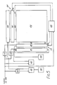
- FIG. 5 shows a display device with a lattice of pixel elements (indicated generally at 20) and a first versatile shift arrangement 22 for selecting the addressing of the rows via a plurality 23 of drivers and XOR gates and a second versatile shift arrangement 24 for selecting the addressing of the columns via a plurality 25 of drivers and XOR gates.
- Each versatile shift arrangement 22, 24 comprises first register means 26, 28 and second register means 30, 32.
- a control input 34 to the second register means 30 for addressing the rows is held high so that this register means 30 is in bypass mode.
- a control input 36 to the second register means 32 for addressing the columns is held low so that this register means 32 is effective as a set of transparent latches.
- a signal is received from a video source 38 corresponding to one picture in length and stored in a column data RAM 40.
- the order in which the pixels are to be written is determined by an address ROM 41.
- a mask data ROM 42 determines the position of the members of a group to be addressed in a non-sequential group addressing scheme. This information is loaded serially into the first shift register means 26 of the row versatile shift arrangement 22.
- a strobe bit from a scan data ROM 44 is loaded into the second shift register means, its position determining which of the rows or collections of rows is to be strobed as outlined hereinbefore.
- a multiplex controller 48 controls the waveforms to be produced by the column drivers and XOR gates 23, 25 in response to the data loaded into the versatile shift arrangements 22, 24.
- Such a display device as shown in Figure 5 can be addressed by the non-sequential group addressing schemes disclosed in our copending published European Patent Application No. 0261901A and our copending European Patent Applications claiming priority from GB 8728433 and from GB 8728434.
Landscapes
- Engineering & Computer Science (AREA)
- Theoretical Computer Science (AREA)
- Physics & Mathematics (AREA)
- Computer Hardware Design (AREA)
- General Physics & Mathematics (AREA)
- Crystallography & Structural Chemistry (AREA)
- Chemical & Material Sciences (AREA)
- Control Of Indicators Other Than Cathode Ray Tubes (AREA)
- Liquid Crystal Display Device Control (AREA)
- Control Of El Displays (AREA)
- Control Of Gas Discharge Display Tubes (AREA)
- Liquid Crystal (AREA)
- Vehicle Body Suspensions (AREA)
- Diaphragms For Electromechanical Transducers (AREA)
- Measuring Pulse, Heart Rate, Blood Pressure Or Blood Flow (AREA)
Priority Applications (1)
| Application Number | Priority Date | Filing Date | Title |
|---|---|---|---|
| AT88311386T ATE96566T1 (de) | 1987-12-04 | 1988-12-01 | Anzeigegeraet. |
Applications Claiming Priority (2)
| Application Number | Priority Date | Filing Date | Title |
|---|---|---|---|
| GB878728435A GB8728435D0 (en) | 1987-12-04 | 1987-12-04 | Display device |
| GB8728435 | 1987-12-04 |
Publications (3)
| Publication Number | Publication Date |
|---|---|
| EP0319292A2 true EP0319292A2 (de) | 1989-06-07 |
| EP0319292A3 EP0319292A3 (de) | 1991-02-06 |
| EP0319292B1 EP0319292B1 (de) | 1993-10-27 |
Family
ID=10628026
Family Applications (1)
| Application Number | Title | Priority Date | Filing Date |
|---|---|---|---|
| EP88311386A Expired - Lifetime EP0319292B1 (de) | 1987-12-04 | 1988-12-01 | Anzeigegerät |
Country Status (7)
| Country | Link |
|---|---|
| US (1) | US5132678A (de) |
| EP (1) | EP0319292B1 (de) |
| JP (1) | JP2726070B2 (de) |
| AT (1) | ATE96566T1 (de) |
| DE (1) | DE3885245T2 (de) |
| ES (1) | ES2045147T3 (de) |
| GB (1) | GB8728435D0 (de) |
Cited By (5)
| Publication number | Priority date | Publication date | Assignee | Title |
|---|---|---|---|---|
| FR2667412A1 (fr) * | 1990-09-28 | 1992-04-03 | Alsthom Gec | Dispositif d'exploitation de donnees issues d'un systeme de traitement de donnees protege contre les erreurs. |
| WO1999026226A1 (en) * | 1997-11-14 | 1999-05-27 | Aurora Systems, Inc. | System and method for reducing peak current and bandwidth requirements in a display driver circuit |
| FR2784489A1 (fr) * | 1998-10-13 | 2000-04-14 | Thomson Multimedia Sa | Procede d'affichage de donnees sur un afficheur matriciel |
| US20100156858A1 (en) * | 2008-12-19 | 2010-06-24 | Su Hwan Moon | Gate driver |
| FR3019366A1 (de) * | 2014-03-26 | 2015-10-02 | Commissariat Energie Atomique |
Families Citing this family (8)
| Publication number | Priority date | Publication date | Assignee | Title |
|---|---|---|---|---|
| JP2734465B2 (ja) * | 1991-04-10 | 1998-03-30 | 三菱電機株式会社 | ネットワーク用入出力装置 |
| US5812148A (en) * | 1993-11-11 | 1998-09-22 | Oki Electric Industry Co., Ltd. | Serial access memory |
| GB2314664A (en) * | 1996-06-27 | 1998-01-07 | Sharp Kk | Address generator,display and spatial light modulator |
| JP3881477B2 (ja) | 1999-09-06 | 2007-02-14 | 沖電気工業株式会社 | シリアルアクセスメモリ |
| CN100360732C (zh) * | 2002-06-11 | 2008-01-09 | 乐金电子(天津)电器有限公司 | 具有烘干功能的家电产品以及其控制方法 |
| JP3901048B2 (ja) * | 2002-07-24 | 2007-04-04 | 日本ビクター株式会社 | アクティブマトリクス型液晶表示装置 |
| JP2010164830A (ja) * | 2009-01-16 | 2010-07-29 | Renesas Electronics Corp | 表示ドライバのデータ線駆動装置 |
| US10652456B2 (en) * | 2017-05-31 | 2020-05-12 | Intel IP Corporation | Image sensor operation |
Family Cites Families (11)
| Publication number | Priority date | Publication date | Assignee | Title |
|---|---|---|---|---|
| JPS5345654B2 (de) * | 1971-08-26 | 1978-12-08 | ||
| US3949391A (en) * | 1974-05-21 | 1976-04-06 | Bell Telephone Laboratories, Incorporated | Plasma panel light pen tracking using adaptive tracking scan |
| JPS53105317A (en) * | 1977-02-25 | 1978-09-13 | Hitachi Ltd | Luminance adjusting circuit |
| US4277783A (en) * | 1979-07-02 | 1981-07-07 | Bell Telephone Laboratories, Incorporated | Light pen tracking method and apparatus |
| JPS57114190A (en) * | 1981-01-07 | 1982-07-15 | Hitachi Ltd | Matrix display device |
| JPS57200091A (en) * | 1981-06-03 | 1982-12-08 | Hitachi Ltd | Matrix display unit |
| JPH0654416B2 (ja) * | 1983-12-23 | 1994-07-20 | 株式会社日立製作所 | 液晶駆動装置とそれを用いた液晶表示装置 |
| JPS60257497A (ja) * | 1984-06-01 | 1985-12-19 | シャープ株式会社 | 液晶表示装置の駆動方法 |
| US4691200A (en) * | 1984-10-01 | 1987-09-01 | Xerox Corporation | Matrix display with a fast cursor |
| JPS62251795A (ja) * | 1986-04-25 | 1987-11-02 | セイコーインスツルメンツ株式会社 | カラ−液晶表示装置のインタ−フエ−ス回路 |
| GB8622717D0 (en) * | 1986-09-20 | 1986-10-29 | Emi Plc Thorn | Display device |
-
1987
- 1987-12-04 GB GB878728435A patent/GB8728435D0/en active Pending
-
1988
- 1988-12-01 EP EP88311386A patent/EP0319292B1/de not_active Expired - Lifetime
- 1988-12-01 DE DE88311386T patent/DE3885245T2/de not_active Expired - Lifetime
- 1988-12-01 ES ES88311386T patent/ES2045147T3/es not_active Expired - Lifetime
- 1988-12-01 AT AT88311386T patent/ATE96566T1/de not_active IP Right Cessation
- 1988-12-05 JP JP63306207A patent/JP2726070B2/ja not_active Expired - Lifetime
-
1991
- 1991-11-12 US US07/789,811 patent/US5132678A/en not_active Expired - Lifetime
Cited By (8)
| Publication number | Priority date | Publication date | Assignee | Title |
|---|---|---|---|---|
| FR2667412A1 (fr) * | 1990-09-28 | 1992-04-03 | Alsthom Gec | Dispositif d'exploitation de donnees issues d'un systeme de traitement de donnees protege contre les erreurs. |
| WO1999026226A1 (en) * | 1997-11-14 | 1999-05-27 | Aurora Systems, Inc. | System and method for reducing peak current and bandwidth requirements in a display driver circuit |
| FR2784489A1 (fr) * | 1998-10-13 | 2000-04-14 | Thomson Multimedia Sa | Procede d'affichage de donnees sur un afficheur matriciel |
| EP0994459A1 (de) * | 1998-10-13 | 2000-04-19 | THOMSON multimedia | Verfahren zur Datenanzeige auf einer Matrixanzeigevorrichtung |
| US6392631B1 (en) | 1998-10-13 | 2002-05-21 | Thomson Licensing S.A. | Process for displaying data on a matrix display |
| US20100156858A1 (en) * | 2008-12-19 | 2010-06-24 | Su Hwan Moon | Gate driver |
| US8368634B2 (en) * | 2008-12-19 | 2013-02-05 | Lg Display Co., Ltd. | Gate driver for partially driving a screen |
| FR3019366A1 (de) * | 2014-03-26 | 2015-10-02 | Commissariat Energie Atomique |
Also Published As
| Publication number | Publication date |
|---|---|
| DE3885245T2 (de) | 1994-04-28 |
| US5132678A (en) | 1992-07-21 |
| JP2726070B2 (ja) | 1998-03-11 |
| JPH02894A (ja) | 1990-01-05 |
| GB8728435D0 (en) | 1988-01-13 |
| EP0319292A3 (de) | 1991-02-06 |
| ES2045147T3 (es) | 1994-01-16 |
| EP0319292B1 (de) | 1993-10-27 |
| DE3885245D1 (de) | 1993-12-02 |
| ATE96566T1 (de) | 1993-11-15 |
Similar Documents
| Publication | Publication Date | Title |
|---|---|---|
| US5307085A (en) | Display apparatus having shift register of reduced operating frequency | |
| EP0319293B1 (de) | Anzeigegerät | |
| US5170158A (en) | Display apparatus | |
| US6040815A (en) | LCD drive IC with pixel inversion operation | |
| EP0496532B1 (de) | Flüssigkristallanzeigegerät | |
| US5103218A (en) | Source electrode driving circuit for matrix type liquid crystal display apparatus | |
| EP0319292B1 (de) | Anzeigegerät | |
| JP3325780B2 (ja) | シフトレジスタ回路および画像表示装置 | |
| US4149151A (en) | Display data synthesizer circuit | |
| US5010325A (en) | Driving network for TFEL panel employing a video frame buffer | |
| US6307531B1 (en) | Liquid crystal display having driving integrated circuits in a single bank | |
| EP0435661A2 (de) | Spaltenelektrodetreiberschaltung für ein Anzeigegerät | |
| EP0319291B1 (de) | Anzeigegerät | |
| JPH07311564A (ja) | 液晶表示パネルの階調駆動装置 | |
| US6188377B1 (en) | Internal row sequencer for reducing bandwidth and peak current requirements in a display driver circuit | |
| JP2747583B2 (ja) | 液晶パネルの駆動回路及び液晶装置 | |
| US6232940B1 (en) | Picture data transfer control apparatus and display apparatus | |
| KR960008102B1 (ko) | 표시장치의 행전극 구동회로 | |
| EP0544427B1 (de) | Steuerschaltung für eine Anzeigeeinheit mit digitaler Sourcesteuerung zur Erzeugung von Mehrfachpegelsteuerspannungen aus einer einzelnen externen Energiequelle | |
| EP0700027B1 (de) | Anzeigeeinheit | |
| JPH07140439A (ja) | 表示装置 | |
| US20020036634A1 (en) | Internal row sequencer for reducing bandwidth and peak current requirements in a display driver circuit | |
| KR100304867B1 (ko) | 주사방식의가변이가능한액정표시장치 | |
| KR100212282B1 (ko) | 도트 반전 방식의 액정 표시 장치의 계조 전압 선택 및 반전 회로 | |
| JP2570259B2 (ja) | 多出力ドライバ |
Legal Events
| Date | Code | Title | Description |
|---|---|---|---|
| PUAI | Public reference made under article 153(3) epc to a published international application that has entered the european phase |
Free format text: ORIGINAL CODE: 0009012 |
|
| AK | Designated contracting states |
Kind code of ref document: A2 Designated state(s): AT BE CH DE ES FR GB GR IT LI LU NL SE |
|
| PUAL | Search report despatched |
Free format text: ORIGINAL CODE: 0009013 |
|
| AK | Designated contracting states |
Kind code of ref document: A3 Designated state(s): AT BE CH DE ES FR GB GR IT LI LU NL SE |
|
| 17P | Request for examination filed |
Effective date: 19910617 |
|
| 17Q | First examination report despatched |
Effective date: 19920904 |
|
| GRAA | (expected) grant |
Free format text: ORIGINAL CODE: 0009210 |
|
| AK | Designated contracting states |
Kind code of ref document: B1 Designated state(s): AT BE CH DE ES FR GB GR IT LI LU NL SE |
|
| PG25 | Lapsed in a contracting state [announced via postgrant information from national office to epo] |
Ref country code: AT Effective date: 19931027 Ref country code: GR Free format text: LAPSE BECAUSE OF FAILURE TO SUBMIT A TRANSLATION OF THE DESCRIPTION OR TO PAY THE FEE WITHIN THE PRESCRIBED TIME-LIMIT Effective date: 19931027 |
|
| REF | Corresponds to: |
Ref document number: 96566 Country of ref document: AT Date of ref document: 19931115 Kind code of ref document: T |
|
| ITF | It: translation for a ep patent filed | ||
| PG25 | Lapsed in a contracting state [announced via postgrant information from national office to epo] |
Ref country code: SE Effective date: 19931202 |
|
| REF | Corresponds to: |
Ref document number: 3885245 Country of ref document: DE Date of ref document: 19931202 |
|
| PGFP | Annual fee paid to national office [announced via postgrant information from national office to epo] |
Ref country code: ES Payment date: 19931230 Year of fee payment: 6 |
|
| ET | Fr: translation filed | ||
| PG25 | Lapsed in a contracting state [announced via postgrant information from national office to epo] |
Ref country code: LU Free format text: LAPSE BECAUSE OF NON-PAYMENT OF DUE FEES Effective date: 19931231 Ref country code: LI Effective date: 19931231 Ref country code: CH Effective date: 19931231 |
|
| PGFP | Annual fee paid to national office [announced via postgrant information from national office to epo] |
Ref country code: BE Payment date: 19940112 Year of fee payment: 6 |
|
| REG | Reference to a national code |
Ref country code: ES Ref legal event code: FG2A Ref document number: 2045147 Country of ref document: ES Kind code of ref document: T3 |
|
| PLBE | No opposition filed within time limit |
Free format text: ORIGINAL CODE: 0009261 |
|
| STAA | Information on the status of an ep patent application or granted ep patent |
Free format text: STATUS: NO OPPOSITION FILED WITHIN TIME LIMIT |
|
| REG | Reference to a national code |
Ref country code: CH Ref legal event code: PL |
|
| 26N | No opposition filed | ||
| PG25 | Lapsed in a contracting state [announced via postgrant information from national office to epo] |
Ref country code: BE Effective date: 19941231 |
|
| EUG | Se: european patent has lapsed |
Ref document number: 88311386.2 Effective date: 19940710 |
|
| BERE | Be: lapsed |
Owner name: THORN EMI P.L.C. Effective date: 19941231 |
|
| PG25 | Lapsed in a contracting state [announced via postgrant information from national office to epo] |
Ref country code: ES Free format text: LAPSE BECAUSE OF NON-PAYMENT OF DUE FEES Effective date: 19951202 |
|
| REG | Reference to a national code |
Ref country code: GB Ref legal event code: 732E |
|
| NLS | Nl: assignments of ep-patents |
Owner name: CENTRAL RESEARCH LABORATORIES LIMITED |
|
| REG | Reference to a national code |
Ref country code: FR Ref legal event code: TP Free format text: CORRECTION |
|
| REG | Reference to a national code |
Ref country code: GB Ref legal event code: IF02 |
|
| REG | Reference to a national code |
Ref country code: ES Ref legal event code: FD2A Effective date: 19960113 |
|
| PGFP | Annual fee paid to national office [announced via postgrant information from national office to epo] |
Ref country code: NL Payment date: 20071127 Year of fee payment: 20 |
|
| PGFP | Annual fee paid to national office [announced via postgrant information from national office to epo] |
Ref country code: IT Payment date: 20071121 Year of fee payment: 20 |
|
| PGFP | Annual fee paid to national office [announced via postgrant information from national office to epo] |
Ref country code: GB Payment date: 20071026 Year of fee payment: 20 Ref country code: FR Payment date: 20071114 Year of fee payment: 20 |
|
| PGFP | Annual fee paid to national office [announced via postgrant information from national office to epo] |
Ref country code: DE Payment date: 20071128 Year of fee payment: 20 |
|
| REG | Reference to a national code |
Ref country code: GB Ref legal event code: PE20 Expiry date: 20081130 |
|
| PG25 | Lapsed in a contracting state [announced via postgrant information from national office to epo] |
Ref country code: NL Free format text: LAPSE BECAUSE OF EXPIRATION OF PROTECTION Effective date: 20081201 |
|
| PG25 | Lapsed in a contracting state [announced via postgrant information from national office to epo] |
Ref country code: GB Free format text: LAPSE BECAUSE OF EXPIRATION OF PROTECTION Effective date: 20081130 |