EP0319668A2 - Prioritätsnetzwerk zur Auflösung von internen und externen Anforderungen für ein asynchrones Bussystem - Google Patents
Prioritätsnetzwerk zur Auflösung von internen und externen Anforderungen für ein asynchrones Bussystem Download PDFInfo
- Publication number
- EP0319668A2 EP0319668A2 EP88116766A EP88116766A EP0319668A2 EP 0319668 A2 EP0319668 A2 EP 0319668A2 EP 88116766 A EP88116766 A EP 88116766A EP 88116766 A EP88116766 A EP 88116766A EP 0319668 A2 EP0319668 A2 EP 0319668A2
- Authority
- EP
- European Patent Office
- Prior art keywords
- bus
- priority
- local
- request
- units
- Prior art date
- Legal status (The legal status is an assumption and is not a legal conclusion. Google has not performed a legal analysis and makes no representation as to the accuracy of the status listed.)
- Withdrawn
Links
Images


Classifications
-
- G—PHYSICS
- G06—COMPUTING OR CALCULATING; COUNTING
- G06F—ELECTRIC DIGITAL DATA PROCESSING
- G06F13/00—Interconnection of, or transfer of information or other signals between, memories, input/output devices or central processing units
- G06F13/14—Handling requests for interconnection or transfer
- G06F13/36—Handling requests for interconnection or transfer for access to common bus or bus system
- G06F13/368—Handling requests for interconnection or transfer for access to common bus or bus system with decentralised access control
- G06F13/37—Handling requests for interconnection or transfer for access to common bus or bus system with decentralised access control using a physical-position-dependent priority, e.g. daisy chain, round robin or token passing
Definitions
- This invention pertains to apparatus for resolving access to an asynchronous bus on a priority basis. More particularly, it pertains to resolving priorities between a plurality of intra or local requestors for access to the asynchronous bus shared by a plurality of inter or external requestors.
- U.S. Patent No. 4,096,569 the priority logic circuits of the distributed tie-breaking newtork grants bus cycles and resolves simultaneous requests to use the bus on the basis of a unit's physical position on the bus with the lowest priority being given to the last unit on the bus located at the opposite end of the bus.
- U.S. Patent No. 4,559,595 discloses an improvement to the priority logic circuits of U.S. Patent No. 4,096,569.
- the priority logic circuits are modified to allow the lowest priority (i.e., the last unit) to be physically at other than its lowest priority position.
- priority resolver logic circuits are provided within a main memory to resolve possible conflicts between competing requests for access to memory.
- the patent discloses priority resolver logic in which the lowest priority requestor has the shortest logical path through the resolver logic.
- the patent teaches that in a priority resolver, it is also desirable, particularly when resolving competing requests for access to main memory to be able to initiate a cycle as early as possible even before the final resolution as to which one of the completing requests will be granted access to the shared resource. This is accomplished by ORing together all of the outputs of the requestors grant flip-flops, each of which is set at the beginning of each priority resolution cycle when the associated requestor has requested use of the shared resource.
- the signal resulting from such ORing provides an early shared resource initiate signal that indicates that at least one priority level has requested use of the shared resource even though the final winner has not yet been determined. This signal is used to initiate a cycle within the shared resource even before the final priority winner is determined.
- U.S. Patent No. 4,493,036 discloses a priority resolver which is similar to that of U.S. Patent No. 4,600,992. Additionally, the disclosed priority resolver provides for the dynamic adjustment of the priority level among competing requests as conditions require.
- the priority logic circuits for resolving the allocation of the shared memory resource on a priority basis are used in addition to the priority network which is used to resolve completing requests for use of the system's common bus. What this has meant is that the priority resolution of competing requests for access to the common bus which can be viewed as a resource external to the system and the priority resolution of competing requests by internal to the system have proceeded in tandem or in series.
- the above referenced Lemay copending patent application discloses an arrangement for reducing the amount of time for resolving competing requests performed in priority resolution circuits in a serial fashion. This is accomplished by including means in a first priority resolver circuit associated with an adapter which generates an initial access request signal as an input to a second priority resolver circuit associated with a memory before the first circuit has decided which source has been granted access.
- the patent application discloses that the arrangement of Lemay can also be used in resolving competing requests for access to the system bus via an adapter.
- a priority resolver circuit similar to the second priority resolver circuit is used to combine the requests received from the local requestors into a single request signal.
- This request signal is forwarded to the system bus while the resolver circuit decides which local requestor was to be granted priority when it was established by the bus priority resolver circuit that the adapter has been granted access to the system bus.
- the above objects are achieved in a preferred embodiment of a bus priority resolver constructed according to the teachings of the present invention.
- the bus priority resolver is used in a data processing system which has a plurality of units, including a bus interface unit (BIU), each of which couple to different physical positions along an asynchronous common system bus.
- BIU bus interface unit
- the BIU couples to a plurality of local units which in turn connect in common to a high speed local bus.
- the asynchronous system bus includes a distributed tie-breaking priority network which consists of a plurality of like priority network sections.
- the bus priority resolver of the present invention incorporates the priority network section which has the highest positional priority access to the asynchronous system bus.
- the priority network section is constructed so as to be easily expandable for accommodating requests from a maximum number of local units.
- the bus priority resolver includes a local priority resolution circuit for generating an output signal for indicating when the highest priority local unit has been granted access to the common bus.
- the local priority resolution circuit is constructed to resolve priority between competing local or internal requests within a minimum amount of time. This minimum time is selected to be just long enough to permit any related operations to be performed, such as parity generation, to filter out any spikes and to resolve the competing local requests.
- the invention utilizes the same request signal generated by the bus priority resolver to request the use of the asynchronous bus. This permits the priority resolution of competing external requests by the bus priority resolver and by the local priority resolution circuit to proceed in parallel. This ensures that access to the system bus will always occur within a single system bus resolution cycle of operation. Following the minimum resolution time of the local priority resolution circuit, the generated output signal is used to set a common grant flip-flop denoting that one of the local units has been granted use of the bus. The identity of the local unit is obtained directly from the bus priority network section request flip-flops.
- the preferred embodiment permits certain types of local units (e.g. CPU) to specify how its request is to be processed. That is, the local unit can specify whether the request has a high or low priority. This facilitates the processing of requests as well as enabling the BIU to exploit fully its high priority positioning on the asynchronous common bus. Also, as in some prior art systems, BIU can service both high and low priority requests from memory and CPU local units.
- local units e.g. CPU
- the arrangement of the present invention minimizes the time required for resolving priorities heretofore resolved in series or partially in series in prior art systems.
- the present invention ensures that a local unit is granted use of the bus within a single system bus resolution cycle of operation. It also includes the expansion capability of prior systems and maximizes the use of existing bus tie-breaking priority networks.
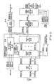
- FIG. 1 shows a data processing system 10 which includes a plurality of identical central processing units (CPUs) 14 through 16, a cache memory 18 and a plurality of memory controllers 20 and 28, each of which controls the operation of a number of memory modules included therein. All of these units couple in common to a high speed local bus 12 as shown.
- CPUs central processing units
- cache memory a cache memory
- memory controllers 20 and 28 each of which controls the operation of a number of memory modules included therein. All of these units couple in common to a high speed local bus 12 as shown.
- the high speed local bus 12 couples through a bus interface unit (BIU) 30 to a system bus 11.
- BIU bus interface unit
- a plurality of different subsystems also couple in common to system bus 11.
- the illustrative different subsystems include a disk controller 32 and a local area network controller 34.
- Each of the subsystems and BIU 30 includes an interface area which enables the unit or units associated therewith to transmit or receive requests in the form of commands, interrupts, data or responses/status to another unit or system bus 11 in an asynchronous manner.
- the system bus 11 further includes a termination network, not shown, located at the left end of bus 11. This network defines the high priority end of bus 11.
- BIU 30, which is positioned next to the termination network, has the highest priority.
- bus priority decreases as a function of each unit's distance from the left end (i.e., termination network).
- the memory is given the highest priority and the central processing unit is given the lowest priority, since it has the lowest real time constraints in contrast with the other units positioned on the system bus as a function of their performance requirements.
- the CPU is the heaviest user of the bus, it is desirable that it be positioned as close to memory as possible.
- the CPU interface circuits are modified to allow a lowest priority CPU to be physically positioned on the system bus next to the system's memory subsystem. This type of arrangement is described in the above referenced patents such as U.S. Patent No. 4,559,595.
- the BIU 30 has a modified interface which also allows it from the point of use of system bus 11 to be viewed logically as if it were connected to the other end of the bus 11. Thus, it includes the same type of functionality as mentioned above while applying it in a different fashion in terms of being able to service requests applied to local bus 12 from the n plurality of CPUs 14 through 16 and the different memory units 18 through 28.
- the BIU 30, includes a system bus priority network 30-10, a local priority network 30-20, a plurality of user flip-flops 30-15 and common user grant flip-flops. Additionally, BIU 30 includes a plurality of blocks 30-40, each having a mailbox register and decoder circuit. Each block 30-40 further includes at least one user flip-flop 30-15. Each mailbox register is connected to receive and store at least one request in the form of a command or data applied to local bus 12 by a CPU or memory unit.
- the left most block 30-40 is used exclusively as a CPU mailbox for both high and low priority requests received from any one of the n CPU'S. As such, it includes both high priority and low priority requests flip-flops 30-15 and low priority request flip-flops which are connected to receive the request signals CPHASK+00 and CPLASK+00 from any one of the CPUs 14 through 16 which enables the accompanying request applied to local bus 12 to be loaded into the corresponding mailbox register 30-40.
- the right most block 30-40 is used as a memory mailbox for high priority memory requests. It includes a user flip-flop which is connected to receive request signal MEMASK+00 from any one of the memory controllers 20 through 28 which enables the accompanying request to be loaded into the corresponding mailbox register 30-40.
- each mailbox register 30-40 are connected to be applied to system bus 11 via a common set of driver circuits included in block 30-50. While the outputs of each mailbox register connect in common, only one of the mailbox registers, which is designated by the system priority network 30-10 to have been granted access to system bus 12, will be enabled to apply signals to the driver circuits of block 30-50.
- signals received directly from the system priority network 30-10, together with any other required signals, are decoded by the decoder circuits included as part of the mailbox register.
- the output from the decoder circuit of the designated requestor is used to enable the requestor's mailbox register for applying the request to system bus 12 upon the setting of grant flip-flop 30-30.
- the remaining mailbox registers are disabled from applying output signals. This can be implemented through the use of tristate registers as is well known in the art. However, no further details as to the specific implementation of the mailbox registers are deemed necessary for an understanding of the present invention.
- FIG. 2 shows in block diagram form, the organization of the system priority network 30-10 of Figure 1.
- the network 30-10 serves as the interface between system bus 11 and the local bus user requestor units.
- the priority network 30-10 includes a request input section 30-100, a logical OR section 30-200 and a priority network section 30-300.
- the request input section 30-100 serves as the primary user interface. As such, it receives request signals from any one of user ask flip-flops which are included within the blocks 30-15.
- section 30-100 there are three users or requestors which can apply request signals MEMASK+00, MPHASK+00 and MPLASK+00 as inputs to section 30-100, in response to local bus request signals MYIACK+00, CPHASK+00 and CPLASK+00.
- section 30-100 In response to user requests, section 30-100 generates a corresponding number of output request signals MMREQT-00 and MPREQT-00 which are applied as inputs to logical OR section 30-200. The same signals are also applied as inputs to priority network section 20-300.
- section 30-100 applies output signals designating which user or requestor has been granted access to system bus 11. These signals are derived directly from the states of the request flip-flops included in section 30-100 as explained herein in greater detail. In the system of Figure 1, these signals correspond to signals MMREQT+ and MPREQT+ which are applied to decoder circuits of blocks 30-40. As explained herein, since there are signals which uniquely designating memory and CPU requestors, these signals can be used directly to identify the requestor which has been granted access to system bus 11.
- the request input section 30-100 also receives bus and priority network signals from priority network section 30-300. These include signals bus data cycle now signal BSDCNN-20, bus idle signal BSIDLE+00, priority network busy signal PRIBSY-00 and bus master clear signal BSMCLR-20.
- Priority network section 30-300 forms a part of the distributed priority network of system bus 11 and operates as the other sections to resolve conflicts between competing external requests received in the form of signals BSREQL+10 and BSREQH+10 for access to system bus 11.
- priority network section 30-300 Based upon any conflict, priority network section 30-300 generates signals PRIBSY-00 and BSMYOK+10.
- the signal BSMYOK+10 when forced to a binary ONE signals that BIU 30 is granting permission to use system bus 11 to any other unit of lower priority.
- This signal is applied as one of the physically skewed or diagonal lines corresponding to the set of priority network signals used by each unit connected to system bus 11.
- priority network section 20-300 in response to bus data cycle now signal BSDCNN+10, generates a bus delayed signal BSDCNB-20 which is applied as an input to logical OR section 30-200.
- the logical OR section 30-200 generates an output request signal MYREQT+00 by logically ORing together the input signals MMREQT-00 and MPREQT-00.
- the signal MYREQT+00 is generated at the earliest possible time and is simultaneously applied to system bus 11 and to local priority resolution network 30-20. As explained herein, this allows the resolution of both external and internal or local requests to proceed in parallel. This ensures that access to system bus 11 by the highest priority local unit takes place within a single system bus resolution cycle of operation.
- local priority bus resolution network 30-20 in response to signals MYREQT+00 and BSDCNB-20, generates as an output, my data cycle now set signal MYDCNS-00. As explained herein, this signal is generated within a minimum of time which also permits the requesting local unit to carry out and complete whatever operations it requires, so that it can immediately access the system bus 11 at the end of the system bus resolution cycle.
- the signal MYDCNS-00 is used to set the shared or common user grant flip-flop of block 30-30. This results in the generation of my data cycle now grant signal MYDCNN+10 which is in turn applied to system bus 11 via one of the driver circuits of block 30-50.
- the grant signal MYDCNN+10 is also applied to an enabling input of the appropriate bus address and data driver circuits for applying the local request from the mailbox register of the highest priority local unit.
- grant flip-flop 30-30 also receives bus acknowledgement, negative acknowledgement and wait response signals BSACKR+10, BSNAKR+10 and BSWAIT+10 as inputs, in addition to bus master clear signal BSMCLR-20. These signals are used to reset the user grant flip-flops 30-30 in a conventional manner following the receipt of a response to the transmitted request by the unit designated in the request.
- the system bus 11 communication proceeds on a master-slave basis. That is, any unit desiring to communicate requests a bus cycle which is granted on a priority basis. When the bus cycle is granted, that unit becomes the master and may address any other unit on system bus 11 as the slave.
- the addressed or slave unit can make any one of the above three possible responses (i.e., ACK, NACK or WAIT). Any one of these responses causes the grant flip-flop 30-30 to be reset.
- ACK acknowledge
- NACK NACK
- WAIT grant flip-flop
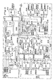
- FIG. 3 shows in greater detail, each of the blocks of Figure 2.
- block 30-15 includes the user flip-flops for the plurality of local CPUs 14 through 16 and memory controllers 20 through 28. More specifically, a first memory user flip-flop 30-150a is connected to be set to a binary ONE state in response to a memory ask signal MMASKH+00 generated by any one of the memory controllers 20 through 28. Similarly, it is reset to a binary ZERO state when signal MMASKR-00 is forced to a binary ZERO upon the completion of the memory request.
- the second user flip-flop 30-150b is connected to be set to a binary ONE state in response to a CPU user high priority system bus request signal CPHASK+00 received via bus 10 from any one of the local CPUs 14 through 16.
- the third user flip-flop 30-150c is connected to be set to a binary ONE state in response to a CPU user request low priority system bus request signal CPLASK+00 received from any local CPUs 14 through 16.
- Both flip-flops 30-150b and 30-150c are reset to binary ZEROS in response to signal MPASKR-00 being forced to a binary ZERO state.
- Signal MPASKR-00 is forced to a binary ZERO when processing of the request has been completed.
- the priority network section 30-300 includes a sixty (60) nanosecond delay circuit 30-302 which is connected to delay bus data cycle now signal, BSDCNN+10, received from system bus 11 prior to being applied as one input an OR gate 30-304.
- the sixty (60) nanosecond period enables the highest priority requesting unit to utilize the next bus cycle without interference.
- the receiving unit or slave uses this signal as a synchronizing signal.
- the OR gate 30-304 combines signal BSDCNN+10 and the output of delay circuit 30-302 to produce a strobe signal BSDCNB+00. This signal is used to clear the priority network section 20-300 between system bus cycles. This strobe signal delayed 60 nanoseconds from the positive edge of bus data cycle now signal, BSDCNN+10.
- an inverter circuit 30-306 inverts signal BSDCNN+10 to generate signal BSDCNN-20 which is used to prevent the setting of the memory and CPU request flip-flops 30-102 and 30-104 of section 30-100 during a current system bus cycle of operation preventing any interference.
- a NOR gate 30-308 combines bus high priority and low priority request signals BSREQH+10 and BSREQL+10 to generate bus request signal BSREQT-00.
- signal BSREQT-00 switches from a binary ONE to a binary ZERO, it causes inverting AND gate 30-310 to force priority network request signal PRIREQ+00 to a binary ONE in the absence of signal BSDCNB+00.
- Signal PRIREQ+00 remains a binary ONE until signal BSDCNB+00 is forced to a binary ONE.
- the signal PRIREQ+00 defines when the distributed system priority network of bus 11 switches from an idle state to a busy state. That is, signal PRIREQ+00 is applied to a twenty (20) nanosecond delay circuit 30-314 which generates signal PRIREQ+20 which causes a NOR gate 30-316 to hold prinet busy signal PRIBSY-00 at a binary ZERO indicative of a busy state. Signal PRIBUSY-00 prevents storage of any requests by section 30-100 generated by the local units user during a priority network resolution cycle.
- the 20 nanosecond delay 20-314 includes sufficient delay to compensate for the propagation delays of circuits 30-316, 30-112/30-106 and 30-104/30-102.
- Signal PRIREQ+20 also causes an AND gate 20-318 to force bus my OK signal BSMYOK+00 to a binary ONE in the absence of a system bus request having been received by BIU 30 (i.e., signals MMREQT-00 and MPREQT-00 are binary ONES).
- Signal BSMYOK+00 is applied via a diode and inductor filter/slope control circuit included in driver circuit 30-50 to system bus 11.
- Signal BSMYOK+00 allows the other I/0 units (i.e., controllers 32 and 34) to win access to system bus 11 if BIU 30 has not received a request after a 20 nanosecond delay established by delay circuit 30-314.
- signal BSMYOK+00 is applied to line BSMYOK of the nine skewed lower priority network lines to indicate to the next lower priority unit (i.e., controller 32) and succeeding lower priority units (i.e., controller 34) that there is no higher priority unit which is requesting use of the next bus cycle thereby allowing all such lower priority units to use the next bus cycle.
- signal BSMYOK+10 is one of the priority signals which are applied as input to the grant flip-flop of each lower priority unit.
- signal BSDCNB+00 is applied via an inverter circuit 20-322 as an input to local priority network 30-20.
- Signal BSDCNB-20 prevents the setting of the grant flip-flop 30-30 during the period of time that each of the priority network sections are being cleared.
- Signal BSDCNB+00 is also applied as one input of an inverting AND gate 30-312.
- Gate 30-312 forces bus idle signal BSIDLE+00 to a binary ONE in the absence of a request from any unit coupled to system bus 11 (i.e., signals BSREQL+10 and BSREQH+10 are binary ZEROS) during the time interval when the priority network sections are not being cleared (i.e., signal BSDCNB+00 is a binary ZERO).
- Signal BSIDLE+00 as explained herein allows BIU 30 to have the lowest priority on the system bus 11 while being positioned at the highest priority end of system bus 11.
- Request Input Section 30-100 includes a main memory (MM) request flip-flop 20-104 and a microprocessor (MP) request flip-flop 20-102. Both flip-flops 30-102 and 30-104 are implemented by 74F type flip-flop elements so as to reduce any possibility of oscillation produced by the occurrence of an asynchronously applied input signal having a minimum width. Memory request flip-flop 30-104 is set to a binary ONE state when a NAND gate 30-112 forces signal MMREQS-00 to a binary ZERO.
- Memory request flip-flop 30-104 is reset to a binary ZERO state in response to signal MMASKR-00 being forced to a binary ZERO by the corresponding local unit.
- the main memory request signal MMREQT+00 has the highest priority on system bus 11 by the positioning of BIU 30 within the highest bus socket location.
- the microprocessor flip-flop 30-102 has its data input terminal connected to ground so as to be reset to a binary ZERO on the trailing edge of signal MYDCNN-00 in the absence of any high priority or low priority microprocessor request (i.e., signal MPREQS-00 is a binary ZERO).
- the output signals MMREQT-00 and MPREQT-00 from request input section 30-100 are applied as inputs to the CPU and memory mailbox register circuits 30-40 for designating which local unit has been granted access as explained herein. Additionally, signals MMREQT-00 and MPREQT-00 are applied to the inverting inputs of an OR gate of logical OR section 30-200. Gate 30-200 logically OR'S both request signals to produce a resulting my request output signal MYREQT+00. The signal MYREQT+00 is simultaneously applied as an input to local priority network 30-20 and to system bus 11 via an inverter driver circuit of block 30-50 and line BSREQH-.
- my request signal MYREQT+00 is applied to a 30 nanosecond local priority resolver delay circuit 30-22.
- the delay circuit 30-22 defines the minimum time required for resolving any conflicts between memory and CPU requests on a priority basis.
- the delay circuit 30-22 also filters out any spikes produced by request signals MMREQT-00 and MPREQT-00 and permits sufficient time for checking and multiplexing of request data, address and commands received from the main memory and CPU local bus requestors.
- Signal MYDCNS-00 is used to set to a binary ONE, a pair of flip-flops 30-300 and 30-302 which make up grant flip-flop 30-30.
- the negation output signals MYDCNN-00 and MYDCNN-01 are applied to the inverting inputs of an AND gate 30-304 which generates my data cycle now, signal MYDCNN+10.
- the negation outputs of flip-flops 30-300 and 30-302 are used to avoid spikes or signal glitches.
- the clock (c) and data (d) inputs of both flip-flops are tied to a voltage +V to reduce spikes or signal glitches. Both flip-flops are reset to binary ZEROS when reset signal MYDCNR-00 is forced to a binary ZERO.
- Signal MYDCNR-00 when a binary ZERO, also inhibits flip-flops 30-300 and 30-302 from being set.
- Signal MYDCNR-00 is forced to a binary ZERO when either bus master clear signal BSMCLR-20 or bus response signal BSRESP-20 applied to one of the inverting inputs of NOR gate 30-306 is a binary ZERO.
- each unit's priority network Associated with each unit's priority network is a grant flip-flop. At any point in time, only one specified grant flip-flop may be set and the unit is deemed the "master" for that specific bus cycle. Each unit may make a user request to use the system bus 11 resulting in the setting of its user or ask flip-flop. Therefore, at any time, many user flip-flops may be set, each representing a request for a future bus cycle. Additionally, each unit connected to system bus 11 has a request flip-flop. The request flip-flops of all units collectively may be viewed as a request register. And, it is the outputs of this request register that supply the distributed bus priority network sections of system bus 11 and establish that only one grant flip-flop will be set no matter how many requests are pending at the time. If there are no requests pending, then no request flip-flops will be set.
- the first unit to set its user or ask flip-flop causes its request flip-flop to set. This, in turn, inhibits the other units from setting their request flip-flops after a period of delay. Thus, a number of request flip-flops may be set during this delay period depending upon the arrival of such requests.
- a particular grant flip-flop is set when the unit associated therewith had set its request flip-flop, and there is no higher priority unit which has requested use of the system bus during the bus cycle.
- the first interval is the period of time required to determine the highest priority unit which is to be granted the bus cycle (i.e., the unit which has won the system bus). This interval corresponds to the priority network resolution cycle which starts at the negative going edge of bus request signal BSREQT-00. The interval ends following the amount of asynchronous delay allowed within the system for priority to settle and for the selection of the highest priority unit requesting use of system bus 11.
- the next interval is the period during which the master unit calls the slave unit or stated differently transfers the request to system bus 11.
- This interval starts at the negative going edge of bus data cycle, now signal BSDCNN-00.
- the transition indicates that the use of system bus 11 has been granted to a master unit.
- the master unit is free to transfer a request to another or slave unit in the form of information applied to the address, data and control lines of system bus 11.
- the last interval is the period of time allocated for the response by the slave or receiving unit. This interval begins at the negative going edge of the strobe signal BSDCNB-20 which corresponds to bus signal BSDCND-00. During this interval, the slave unit determines if the address designates such slave unit and stores the address, data and command information applied to the system bus 11. It then begins the process of determining the type of response to be made to the request. The end of the third interval, which is also the end of the bus cycle, corresponds to the point at which the bus data cycle, now signal BSDCNN-00, switches to a binary ONE.
- the above described intervals are illustrated in Figure 4.
- the first interval is the one which is pertinent to the present invention.
- the other intervals are shown to illustrate the overall timing of a bus cycle and the reason that any delay in gaining access to system bus 11 by the local bus units could result in less frequent system bus cycles being granted to such units.
- the priority resolution apparatus of the present invention permits all local unit requests to be resolved within a single system bus resolution cycle thereby eliminating the possibility of any delay which would result in the loss of system bus cycles by such local units. Additionally, the priority resolution apparatus of the present invention is organized to service requests from any number of user local units which share a common grant flip-flop section.
- CPU 14 Normally, CPU 14 only generates a bus request when it is ready to transmit or receive data to or from one of the I/O units connected to system bus 11. When CPU 14 wants to access data stored on disk controller 32, it generates a bus request on local bus 12. At the same time, CPU 14 forces signal CPHASK+00 to a binary ONE. This causes the request to be loaded into CPU mailbox register 30-40 and high priority request user ask flip-flop 30-150b of Figure 3 to be set to a binary ONE. As seen from Figure 4, ASK flip-flop 30-150b forces signal MPASKH+00 to a binary ONE. This results in NAND gate 20-106 of Figure 3 forcing signal MPREQS-00 to a binary ZERO.
- the request input section 30-100 stores the local user request in the corresponding request flip-flop.
- signal MPREQT-00 is forced to a binary ZERO as shown in Figure 4.
- the setting of one of the request flip-flops in request input section 20-100 causes the OR gate 30-200 of the logical OR section to force my request signal MYREQT+00 to a binary ONE.
- Signal MYREQT+00 is simultaneously applied to system bus 11 via driver circuit 30-50 and to local priority network 30-20.
- system bus request signal BSREQH-00 from a binary ONE to a binary ZERO which signals the start of a system bus priority network resolution cycle of operation.
- the priority network sections comprising the distributed priority bus network of system bus 11 then operate to resolve the relative positional priorities of those units requesting simultaneous access to bus 11.
- BIU 30 Since BIU 30 has the highest priority by being positioned at the highest location on system bus 11, it will be granted access to system bus 11 under the control of network 30-10 following the completion of the system bus resolution cycle. It will also be noted that the setting of MP request flip-flop 20-102 causes AND gate 30-318 of Priority Network Section 30-300 to force signal BSMYOK+10 to a binary ZERO. This indicates to controlle.r units 32 and 34 that BIU 30 will be using the next system bus cycle thereby inhibiting such units from using system bus 11 during this time.
- AND gate 20-304 forces signal MYDCNN+10 to a binary ONE.
- the output MYDCNN+10 from the grant flip-flops is applied to the mailbox decode circuits together with the output request signals MMREQT+00 and MPREQT+00. Since these are only two types of local units competing for access, signal MMREQT+00 is only needed to indicate whether or not the local requestor granted the system bus cycle is main memory or a CPU local unit.
- the signal MMREQT+00 is used to select the appropriate mailbox register containing the request to be transferred to bus 10.
- signal MYDCNN+10 applied to system bus 11 results in bus data cycle now signal, BSDCNN00 being forced to a binary ZERO signalling the end of the system bus priority resolution cycle. This, in turn, forces BIU bus signal BSDCNN+10 to a binary ONE. After a delay of 60 nanoseconds, OR gate 30-304 forces signal BSDCNB+00 to a binary ONE which clears the priority network circuits for the next system bus resolution cycle.
- the request input section will accept the low priority request from one of the local CPUs by setting MP request flip-flop 30-102 to a binary ONE state.
- signal MYDCNN-00 causes request flip-flop 30-102 to be reset to a binary ZERO.
- the apparatus of the present invention provides a most efficient system for ensuring that the requests for access to system bus 11 received from the local requestors are all resolved within the priority resolution cycle of system bus 11.
- the apparatus maximizes its use of existing circuits of the system bus interface network 30-10. Further, it permits a local CPU to designate how its request is to be processed. This exploits the dual priority bus positioning afforded to BIU 30 and enables important CPU operations to be carried out on a high priority basis thereby eliminating delays.
- Request Input Section 30-100 the number of request flip-flops included in Request Input Section 30-100 would be expanded to include a request flip-flop for each local CPU or memory user. Also, for accommodating multilevels of simultaneity, each CPU would have its own mailbox addressable by such CPU. The outputs from all of the request flip-flops would be again ORed together by logical OR section 30-200 in the same manner as described above. Additionally, the request flip-flop outputs would be decoded by the mailbox register circuits of each local unit to identify the local unit which was granted access.
- the grant flip-flops of block 30-30 could be implemented as a single shared flip-flop, different types of circuits could be employed, etc.
Landscapes
- Engineering & Computer Science (AREA)
- Theoretical Computer Science (AREA)
- Physics & Mathematics (AREA)
- General Engineering & Computer Science (AREA)
- General Physics & Mathematics (AREA)
- Multi Processors (AREA)
- Bus Control (AREA)
Applications Claiming Priority (2)
| Application Number | Priority Date | Filing Date | Title |
|---|---|---|---|
| US07/129,277 US4901226A (en) | 1987-12-07 | 1987-12-07 | Inter and intra priority resolution network for an asynchronous bus system |
| US129277 | 1987-12-07 |
Publications (2)
| Publication Number | Publication Date |
|---|---|
| EP0319668A2 true EP0319668A2 (de) | 1989-06-14 |
| EP0319668A3 EP0319668A3 (de) | 1991-09-25 |
Family
ID=22439257
Family Applications (1)
| Application Number | Title | Priority Date | Filing Date |
|---|---|---|---|
| EP19880116766 Withdrawn EP0319668A3 (de) | 1987-12-07 | 1988-10-10 | Prioritätsnetzwerk zur Auflösung von internen und externen Anforderungen für ein asynchrones Bussystem |
Country Status (4)
| Country | Link |
|---|---|
| US (1) | US4901226A (de) |
| EP (1) | EP0319668A3 (de) |
| AU (1) | AU611964B2 (de) |
| CA (1) | CA1314332C (de) |
Cited By (1)
| Publication number | Priority date | Publication date | Assignee | Title |
|---|---|---|---|---|
| EP0683459A1 (de) * | 1994-05-13 | 1995-11-22 | Hewlett-Packard Company | Kohärente Transaktionsordnung in einem vielschichtigen Bussystem |
Families Citing this family (13)
| Publication number | Priority date | Publication date | Assignee | Title |
|---|---|---|---|---|
| US5119480A (en) * | 1989-11-13 | 1992-06-02 | International Business Machines Corporation | Bus master interface circuit with transparent preemption of a data transfer operation |
| US5247671A (en) * | 1990-02-14 | 1993-09-21 | International Business Machines Corporation | Scalable schedules for serial communications controller in data processing systems |
| US5241629A (en) * | 1990-10-05 | 1993-08-31 | Bull Hn Information Systems Inc. | Method and apparatus for a high performance round robin distributed bus priority network |
| US5243702A (en) * | 1990-10-05 | 1993-09-07 | Bull Hn Information Systems Inc. | Minimum contention processor and system bus system |
| US5132967A (en) * | 1990-10-29 | 1992-07-21 | International Business Machines Corporation | Single competitor arbitration scheme for common bus |
| US5255383A (en) * | 1991-04-15 | 1993-10-19 | Seagate Technology, Inc. | Method and apparatus for skewing a memory read clock signal in a magnetic disk drive system |
| JPH07122864B2 (ja) * | 1991-07-22 | 1995-12-25 | インターナショナル・ビジネス・マシーンズ・コーポレイション | データ処理システム、データ処理システムに使用するインターフエース回路及びデータ・プロセツサ間の通信方法 |
| US5446847A (en) * | 1991-10-04 | 1995-08-29 | Bull Hn Information Systems Inc. | Programmable system bus priority network |
| US5299315A (en) * | 1992-09-17 | 1994-03-29 | International Business Machines Corp. | Personal computer with programmable threshold FIFO registers for data transfer |
| JP3647055B2 (ja) * | 1993-11-17 | 2005-05-11 | キヤノン株式会社 | 情報処理システム、管理方法および管理装置 |
| JPH1097496A (ja) * | 1996-09-20 | 1998-04-14 | Sanyo Electric Co Ltd | バス制御方法およびその方法を用いた装置 |
| US6052772A (en) * | 1998-04-13 | 2000-04-18 | International Business Machines Corporation | Memory request protocol method |
| WO2014178856A1 (en) * | 2013-04-30 | 2014-11-06 | Hewlett-Packard Development Company, L.P. | Memory network |
Family Cites Families (7)
| Publication number | Priority date | Publication date | Assignee | Title |
|---|---|---|---|---|
| US4006466A (en) * | 1975-03-26 | 1977-02-01 | Honeywell Information Systems, Inc. | Programmable interface apparatus and method |
| US4296464A (en) * | 1977-03-03 | 1981-10-20 | Honeywell Inc. | Process control system with local microprocessor control means |
| US4387425A (en) * | 1980-05-19 | 1983-06-07 | Data General Corporation | Masterless and contentionless computer network |
| US4373183A (en) * | 1980-08-20 | 1983-02-08 | Ibm Corporation | Bus interface units sharing a common bus using distributed control for allocation of the bus |
| US4604685A (en) * | 1982-02-19 | 1986-08-05 | Honeywell Information Systems Inc. | Two stage selection based on time of arrival and predetermined priority in a bus priority resolver |
| US4600992A (en) * | 1982-12-14 | 1986-07-15 | Honeywell Information Systems Inc. | Priority resolver with lowest priority level having shortest logic path |
| US4604689A (en) * | 1983-04-15 | 1986-08-05 | Convergent Technologies, Inc. | Bus repeater |
-
1987
- 1987-12-07 US US07/129,277 patent/US4901226A/en not_active Expired - Fee Related
-
1988
- 1988-10-10 EP EP19880116766 patent/EP0319668A3/de not_active Withdrawn
- 1988-10-31 AU AU24530/88A patent/AU611964B2/en not_active Ceased
- 1988-11-09 CA CA000582593A patent/CA1314332C/en not_active Expired - Fee Related
Cited By (2)
| Publication number | Priority date | Publication date | Assignee | Title |
|---|---|---|---|---|
| EP0683459A1 (de) * | 1994-05-13 | 1995-11-22 | Hewlett-Packard Company | Kohärente Transaktionsordnung in einem vielschichtigen Bussystem |
| US5524216A (en) * | 1994-05-13 | 1996-06-04 | Hewlett-Packard Company | Coherent transaction ordering in multi-tiered bus system |
Also Published As
| Publication number | Publication date |
|---|---|
| CA1314332C (en) | 1993-03-09 |
| US4901226A (en) | 1990-02-13 |
| EP0319668A3 (de) | 1991-09-25 |
| AU611964B2 (en) | 1991-06-27 |
| AU2453088A (en) | 1989-06-08 |
Similar Documents
| Publication | Publication Date | Title |
|---|---|---|
| US5301283A (en) | Dynamic arbitration for system bus control in multiprocessor data processing system | |
| US4785394A (en) | Fair arbitration technique for a split transaction bus in a multiprocessor computer system | |
| US4030075A (en) | Data processing system having distributed priority network | |
| US4320457A (en) | Communication bus acquisition circuit | |
| US5412788A (en) | Memory bank management and arbitration in multiprocessor computer system | |
| EP0383475A2 (de) | Arbitrierung von gemeinsamen Betriebsmitteln | |
| US5276887A (en) | Bus arbitration system for granting bus access to devices following two-wire bus arbitration protocol and devices following three-wire bus arbitration protocol | |
| US4096569A (en) | Data processing system having distributed priority network with logic for deactivating information transfer requests | |
| US6584523B1 (en) | Device for organizing the access to a memory bus | |
| US5842025A (en) | Arbitration methods and apparatus | |
| EP0319668A2 (de) | Prioritätsnetzwerk zur Auflösung von internen und externen Anforderungen für ein asynchrones Bussystem | |
| WO1982002440A1 (en) | Synchronous bus arbiter | |
| JPH0773137A (ja) | 多レベル・バス・アービトレーションのための方法、アダプタおよびシステム | |
| EP0564116A1 (de) | Arbitrierungssteuerung zwischen Wirtsystem und verbundenen Untersystemen | |
| CA1205567A (en) | Distributed priority network logic for allowing a low priority unit to reside in a high priority position | |
| JPH0690701B2 (ja) | 仲裁回路 | |
| US7234012B2 (en) | Peripheral component interconnect arbiter implementation with dynamic priority scheme | |
| US5150466A (en) | Flexible distributed bus priority network | |
| US4376975A (en) | Arbitration controller providing for access of a common resource by a plurality of central processing units | |
| US5983025A (en) | Computer system buffers for providing concurrency and avoid deadlock conditions between CPU accesses, local bus accesses, and memory accesses | |
| US5241629A (en) | Method and apparatus for a high performance round robin distributed bus priority network | |
| US5446847A (en) | Programmable system bus priority network | |
| KR100973419B1 (ko) | 버스 중재 방법 및 장치 | |
| KR20040051608A (ko) | 컴퓨터 시스템 및 컴퓨터 시스템의 작동 방법 | |
| EP0533429B1 (de) | Rechnerbussteuerungssystem |
Legal Events
| Date | Code | Title | Description |
|---|---|---|---|
| PUAI | Public reference made under article 153(3) epc to a published international application that has entered the european phase |
Free format text: ORIGINAL CODE: 0009012 |
|
| AK | Designated contracting states |
Kind code of ref document: A2 Designated state(s): DE FR GB |
|
| PUAL | Search report despatched |
Free format text: ORIGINAL CODE: 0009013 |
|
| AK | Designated contracting states |
Kind code of ref document: A3 Designated state(s): DE FR GB |
|
| 17P | Request for examination filed |
Effective date: 19920316 |
|
| 17Q | First examination report despatched |
Effective date: 19930630 |
|
| RAP1 | Party data changed (applicant data changed or rights of an application transferred) |
Owner name: BULL HN INFORMATION SYSTEMS INC. |
|
| RAP1 | Party data changed (applicant data changed or rights of an application transferred) |
Owner name: BULL HN INFORMATION SYSTEMS INC. |
|
| STAA | Information on the status of an ep patent application or granted ep patent |
Free format text: STATUS: THE APPLICATION IS DEEMED TO BE WITHDRAWN |
|
| 18D | Application deemed to be withdrawn |
Effective date: 19950502 |