EP0320274A2 - Urladekontrollsystem in einem Mehrprozessorsystem - Google Patents
Urladekontrollsystem in einem Mehrprozessorsystem Download PDFInfo
- Publication number
- EP0320274A2 EP0320274A2 EP88311662A EP88311662A EP0320274A2 EP 0320274 A2 EP0320274 A2 EP 0320274A2 EP 88311662 A EP88311662 A EP 88311662A EP 88311662 A EP88311662 A EP 88311662A EP 0320274 A2 EP0320274 A2 EP 0320274A2
- Authority
- EP
- European Patent Office
- Prior art keywords
- cluster
- ipl
- storage unit
- clusters
- control unit
- Prior art date
- Legal status (The legal status is an assumption and is not a legal conclusion. Google has not performed a legal analysis and makes no representation as to the accuracy of the status listed.)
- Granted
Links
Images





Classifications
-
- G—PHYSICS
- G06—COMPUTING OR CALCULATING; COUNTING
- G06F—ELECTRIC DIGITAL DATA PROCESSING
- G06F9/00—Arrangements for program control, e.g. control units
- G06F9/06—Arrangements for program control, e.g. control units using stored programs, i.e. using an internal store of processing equipment to receive or retain programs
- G06F9/44—Arrangements for executing specific programs
- G06F9/4401—Bootstrapping
- G06F9/4406—Loading of operating system
- G06F9/441—Multiboot arrangements, i.e. selecting an operating system to be loaded
-
- G—PHYSICS
- G06—COMPUTING OR CALCULATING; COUNTING
- G06F—ELECTRIC DIGITAL DATA PROCESSING
- G06F15/00—Digital computers in general; Data processing equipment in general
- G06F15/16—Combinations of two or more digital computers each having at least an arithmetic unit, a program unit and a register, e.g. for a simultaneous processing of several programs
- G06F15/177—Initialisation or configuration control
-
- G—PHYSICS
- G06—COMPUTING OR CALCULATING; COUNTING
- G06F—ELECTRIC DIGITAL DATA PROCESSING
- G06F9/00—Arrangements for program control, e.g. control units
- G06F9/06—Arrangements for program control, e.g. control units using stored programs, i.e. using an internal store of processing equipment to receive or retain programs
- G06F9/44—Arrangements for executing specific programs
- G06F9/4401—Bootstrapping
- G06F9/4405—Initialisation of multiprocessor systems
Definitions
- the present invention relates to an initial program load (IPL) control system in a multiprocessor system, and, more particularly, to a method and apparatus for executing the IPL in a multiprocessor system divided into a plurality of clusters.
- IPL initial program load
- a multiprocessor system is constituted by a plurality of processors, and for a cluster control, the plurality of processors is divided into a plurality of groups, each of which is called a "cluster", and then a control of an access between processors is performed through each cluster.
- each cluster is an elemental for processing the access control of the processors.
- the IPL is an initial setting procedure for loading a program, to start an operation of an operating system (OS) from an auxiliary storage (for example, a direct access storage device (DASD)) to a main memory or a local storage unit.
- OS operating system
- auxiliary storage for example, a direct access storage device (DASD)
- an apparatus for executing an initial program load (IPL) between processors constituting a multiprocessor system, the processors being divided into a plurality of clusters comprising: a global storage unit, a global control unit connected to each of the clusters and the global storage unit through a corresponding bus line and for processing an order between the clusters; a memory control unit provided in each of the clusters and connected between the global control unit and each of the processors belonging to each cluster, and for controlling a transmission and reception of the order between the global control unit and the processor; a local storage unit provided in each of the clusters and connected to the memory control unit, for storing data; and a service processor provided in each of the clusters and connected to the memory control unit, for processing the reset operation and an IPL operation; wherein one of the clusters further comprises a direct access storage device connected to the memory control unit, for storing the IPL information.
- IPL initial program load
- a method for executing an initial program load (IPL) control in a multiprocessor system having a global storage unit, a global control unit and a plurality of clusters, each of the clusters having at least one or more processors and a local storage unit, and one of the clusters having a direct access storage device, the method comprising: executing the IPL from the processor belonging to the cluster having the direct access storage device to the local storage unit belonging to that cluster; transferring the IPL information from the local storage unit executing the IPL to the global storage unit; and transferring the IPL information from the global storage unit to the other storage unit in another cluster not having the direct access storage device.
- IPL initial program load
- Apparatus and methods embodying the present invention can be advantageous for large scale numerical simulations in scientific and technical fields in which high speed calculations are necessary.
- FIG. 1 is a schematic block diagram of a previously-proposed multiprocessor system.
- the multiprocessor system is constituted by, for example, processors CPU0 to CPU5, and each processor is connected in parallel to another processor through a bus line BUS and a mutual control is carried out between one processor and the other.
- each processor is set to one of four states having an exclusive relationship therebetween; i.e., any one of four states (“STOP”, “OPERATION”, “LOAD” and “CHECK-STOP”) is set in each processor.
- STOP any one of four states
- OPERATION "LOAD”
- CHECK-STOP When carrying out an access, one processor outputs a sense signal to the other processor, to recognize the state of other processor, receives a response from the other processor involving one of the above four states, and carries out a mutual control in accordance with the above four states.
- FIG. 2 is a basic block diagram of an apparatus for the cluster control in the multiprocessor system.
- a plurality of processors CPU1 to CPUn are divided into “m" groups (1 to m) each having three processors, and each group is called a "cluster".
- MCU1 to MCUm are a memory control unit provided in each cluster and connected between the processor and a global control unit GCU.
- the global control unit GCU controls the access between clusters, as explained in detail hereinafter, and is contained in a global storage unit GSU.
- the state of each cluster is defined by the memory control unit MCU based on the state of the processors belonging to that cluster. Further, the global control unit GCU sets up an order for each cluster and controls the processor, based on the order for each cluster, through the memory control unit MCU.
- FIG. 3 is a schematic block diagram of each cluster according to an embodiment of the present invention.
- the multiprocessor system is constituted by sixty four processors, which are divided into sixteen clusters (CLUSTER1 to CLUSTER16) each having four processors CPU0 to CPU3. Therefore, the global control unit GCU controls only sixteen clusters 1 to 16 through the bus line BUS.
- the clusters 2 to 16 have the same structure and the cluster 1 has a structure different from that of the other clusters 2 to 16.
- the cluster 1 comprises a memory control unit MCU1, four processors CPU0 to CPU3, a local storage unit LSU1, a direct access storage device DASD, a service processor SVP1, an input/output processor IOP, and a channel element CHE connected between the IOP and the DASD.
- each of the clusters 2 to 16 comprises a memory control unit MCU, four processors CPU0 to CPU3, a local storage unit LSU, and a service processor SVP.
- the global control unit GCU is used in common for all clusters 1 to 16, and connected to each cluster through the bus line BUS.
- the processor belonging to each cluster is defined by the four states "STOP”, “OPERATION”, “LOAD” and "CHECK-STOP", and these four states are exclusive therebetween and change under the following conditions.
- the state of the cluster is based on the state of the processors belonging to that cluster, as follows.
- None of the processors in the cluster is in the OPERATION or LOAD state and at least one processor in the cluster is in the STOP state.
- None of the processors is in the STOP, OPERATION or LOAD states. These states further include the states wherein the processor are not connected to each other or none of the processor is supplied with power.
- the cluster When a channel subsystem damage is found in the cluster, the cluster is placed in the SUBSYSTEM-DAMAGE state.
- the SUBSYSTEM-DAMAGE state When the SUBSYSTEM-DAMAGE state is set, the CLUSTER-STOP and CLUSTER-CHECK-STOP states are simultaneously set in the cluster.
- Three main orders are sent to each cluster, defined as follows. Namely, the CLUSTER-SENSE order, the CLUSTER-SYNCHRONOUS-CALL order (floating interruption order), and the CLUSTER-RESET and LOAD order (RESET and IPL order). Further, for example, the CLUSTER-BROADCAST-INTERRUPTION order for accessing the same order to all clusters and the CLUSTER-ASYNCHRONOUS-INTERRUPTION order are used, and these orders are called as a whole a GSIGP order.
- the GSIGP order is mainly used for a floating interruption between the processors, as explained hereinafter.
- the global control unit GCU returns the GSIGP order including the incorrect destination to the memory control unit MCU at the transmission side in the same order as the GSIGP order sent from other cluster. In this case, a flag bit indicating the incorrect destination is added to the order.
- the memory control unit MCU at the transmission side recognizes the flag bit in the GSIGP order received, the MCU returns the same GSIGP order as above to the global control unit GCU as the status information. At that time, the content of the GSIGP order is ignored.
- the global control unit GCU sends the returned status information to the memory control unit MCU at the transmission side as the status information, and the status information received from the destination side in the case of a normal GSIGP order.
- the interface lines between the MCU and the GCU include a signal line for discriminating either the status information or the order from the transferred information.
- the GSIGP order is sent to the memory control unit MCU as the order and that order is returned to the global control unit GCU, and then that order is again returned to the memory control unit MCU as the status information. This is because these procedures make the operation procedures at the GCU and the MCU almost identical regardless of the correctness of the cluster ID.
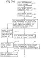
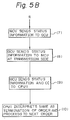
- step (1) Since the procedures from step (1) to step (5) are the same as for the steps shown in Fig. 5, an explanation thereof is omitted. The following step follows step (5).
- step (7) to step (10) are carried out after the above step (6)′. Further, when the interruption enabled processor exists in the cluster at the reception side, the interruption is made to that processor.
- a cluster can be directly re-IPL operated from the global storage unit GSU after an occurrence of errors or an activity of maintenance.
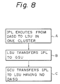
- FIG 8 is a basic flowchart of a method embodying the present invention.
- the IPL operation is executed from the DASD to the LSU in one cluster (step A)
- the IPL information is transferred from the LSU to the GSU (step B)
- the IPL information is transferred from the GCU to the LSU's in the other clusters not having the DASD (step C).
- FIG. 9A is a schematic block diagram of a global control unit GCU according to an embodiment of the present invention.
- the global control unit GCU includes means for transferring the GSIGP orders and means for controlling the access to the global storage unit GSU.
- RCV represents a receiver, PRT a priority circuit, LRCL a logical-to-real cluster translation logic circuit, LRCT a logical-to-real cluster translation table, CCNT a cluster connecting table, CPON a cluster power-ON table, MPX a multiplexer, ECD an encoder, OR an order and DRV a driver.
- the order OR1 comprises a CLUSTER-INVALID (IV), a LOGICAL-CLUSTER-ID (LCI), a command (COM), and a parameter (PRM). Further, the order OR2 comprises a LOGICAL-DRIVE-CLUSTER-ID (LDCI) instead of the LOGICAL-CLUSTER-ID (LCI). RDCI is a REAL-DRIVE-CLUSTER-ID and RRCI is a REAL-RECEIVE-CLUSTER-ID.
- the cluster connecting table CCNT indicates the state of connection of the clusters; the command COM designates the order of the GSIGP; the cluster power-ON table CPON indicates a power-ON/0FF state of the clusters; the driver DRV transfers the order to the cluster; and the encoder ECD encodes the IV bit and the RRCI bit and determines the destination of the processor transferring the order.
- the bit IV indicates the invalidity of the cluster, and is normally "0" when generating the command request and turned ON when the designated cluster does not exist or the power is not turned ON;
- the bit LCI is a logical identifier and the target of the request is designated by the logical cluster number; and the bit LDCI is a logical processor number of the processor generating the request and sets the output of the circuit LRCL.
- the circuit LRCL is a logical block converting a logical cluster number to a physical cluster number.
- the circuit LRCL inputs the bit LCI and outputs the bit RRCI by referring to the table LRCT. In the conversion, the circuit LRCL checks whether or not the designated real cluster is connected and the power of the designated real cluster is turned ON. If the designated cluster is incorrect, the bit IV is turned ON. Further, the circuit LRCL converts the bit RDCI to the bit LDCI.
- the table LRCT refers to the relationship between the logical cluster number and the physical cluster number.
- the multiplexer MPX selects the target cluster.
- the parameter PRM is an additional information to the command COM.
- the priority circuit PRT determines the cluster competition state and gives the priority right to the request.
- the receiver RCV receives the request from the cluster CLU0 to CLU3.
- the bit RDCI is a real cluster number which generated the request and is set by the output of the priority circuit PRT.
- the bit RRCI is a real cluster number indicating the destination of the transferred order and is set by the output of the circuit LRCL.
- Fig. 9B shows means for controlling the access to the GSU and having receivers RCV, a priority circuit PRT, a data access control circuit DACC, a multiplexer MPX, and drivers DRV.
- RCV priority circuit
- PRT priority circuit
- DACC data access control circuit
- MPX multiplexer
- drivers DRV drivers
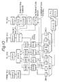
- FIG. 10 is a schematic block diagram of the memory control unit MCU according to an embodiment of the present invention.
- the MCU also includes means for transferring the GSIGP orders and means for controlling the storage access.
- GORV represents a GSIGP order receiver, SCGE a status and condition code generator, GARV a GSIGP acknowledge receiver, GRDV a GSIGP request driver, GRRV a GSIGP request receiver, COEX a command executer, ITPL a interruption pending latch, IOP a I/O processor, SGE a status generator, and GADV a GSIGP acknowledge driver.
- the GSIGP acknowledge receiver GARV is a circuit receiving the acknowledge ACK from the global control unit GCU;
- the status and condition code generator SCGE is a circuit generating the STATUS and CC based on the acknowledge ACK;
- the GSIGP request driver GRDV is a circuit generating the request of the GSIGP to the GCU;
- the priority circuit PRT is a circuit determining the priority of the request when sent from the processor CPU;
- the GSIGP order receiver GORV is a circuit receiving the GSIGP request from the processor CPU and generating the request to the global control unit GCU; and the command executer COEX executes the request sent from the GCU through the GSIGP request receiver GRRV.
- the command executer COEX requests the status generator SGE to generate the status information
- the command executer COEX requests the service processor SVP to generate the status information and to execute the IPL operation, and requests the status generator SGE to also generate the status information.
- the command execute COEX checks the state of the interruption pending latch ITPL. If the interruption pending latch ITPL is turned 0FF, the command executer COEX turns ON the interruption pending latch ITPL and informs the status generator SGE that the ITPL is turned 0FF. If the interruption pending latch ITPL is turned ON, the command executer COEX informs the status generator SGE that the ITPL is turned ON.
- the interruption pending latch ITPL is turned ON by a request from the command executer COEX. Further, the interruption pending latch ITPL supervises the interruption mask to enable the interruption from the processor CPU, detects the processor CPU for which the interrupt mask is turned ON, and interrupts that processor.
- the I/O processor IOP carries out he input/output processing. When a fault occurs at the I/O processor IOP, a SUBSYSTEM-DAMAGE signal is sent to the status generator SGE.
- the service processor SVP carries out a reset of the cluster and the IPL processing, and further, the service processor SVP processes the operator function.
- the status generator SGE generates the status information in accordance with the request from the command executer COEX, and further, takes in the information sent from the service processor SVP and the I/O processor IOP.
- the GSIGP request receiver GRRV receives the GSIGP request from the global control unit GCU, and the GSIGP acknowledge driver GADV returns the generated status information to the cluster which generated the order.
- Fig. 10 shows means for transferring the GSIGP orders and means for controlling the storage access, and having drivers DRV, receivers RCV, a multiplexer MPX, a priority circuit PRT and a data access control circuit DACC.
- the request is transferred to the GCU through the DACC in the MCU.
- the transfer of the IPL information between the LSU and the GSU is carried out by using the above-mentioned data access control circuits which are similar to those of conventional data processing system.
Landscapes
- Engineering & Computer Science (AREA)
- Software Systems (AREA)
- Theoretical Computer Science (AREA)
- Physics & Mathematics (AREA)
- General Engineering & Computer Science (AREA)
- General Physics & Mathematics (AREA)
- Computer Security & Cryptography (AREA)
- Computer Hardware Design (AREA)
- Multi Processors (AREA)
- Stored Programmes (AREA)
- Hardware Redundancy (AREA)
Applications Claiming Priority (2)
| Application Number | Priority Date | Filing Date | Title |
|---|---|---|---|
| JP309455/87 | 1987-12-09 | ||
| JP62309455A JP2753706B2 (ja) | 1987-12-09 | 1987-12-09 | 計算機におけるipl方法 |
Publications (3)
| Publication Number | Publication Date |
|---|---|
| EP0320274A2 true EP0320274A2 (de) | 1989-06-14 |
| EP0320274A3 EP0320274A3 (en) | 1990-05-02 |
| EP0320274B1 EP0320274B1 (de) | 1993-09-29 |
Family
ID=17993197
Family Applications (1)
| Application Number | Title | Priority Date | Filing Date |
|---|---|---|---|
| EP88311662A Expired - Lifetime EP0320274B1 (de) | 1987-12-09 | 1988-12-09 | Urladekontrollsystem in einem Mehrprozessorsystem |
Country Status (6)
| Country | Link |
|---|---|
| US (1) | US5349664A (de) |
| EP (1) | EP0320274B1 (de) |
| JP (1) | JP2753706B2 (de) |
| AU (1) | AU592047B2 (de) |
| CA (1) | CA1319438C (de) |
| DE (1) | DE3884579T2 (de) |
Cited By (8)
| Publication number | Priority date | Publication date | Assignee | Title |
|---|---|---|---|---|
| EP0419920A1 (de) * | 1989-09-26 | 1991-04-03 | Siemens Aktiengesellschaft | Schaltungsanordnung für eine zentralgesteuerte Fernmeldevermittlungsanlage, insbesondere PCM-Fernsprechvermittlungsanlage, mit zentralem Koordinationsprozessor und dezentralen Anschlussgruppen mit Teilsteuerwerken |
| EP0457159A3 (en) * | 1990-05-18 | 1993-06-16 | Fujitsu Limited | Control method for preventing incorrect reset of common resource and multicomputer system executing the method |
| EP0602869A3 (en) * | 1992-12-15 | 1994-08-24 | Ibm | Updating processor control code. |
| EP0683453A1 (de) * | 1994-05-13 | 1995-11-22 | Hitachi, Ltd. | Multiprozessorsystem, dieses System verwendende Plattensteuerung, und nicht unterbrechendes Wartungsverfahren dafür |
| WO1997004385A1 (de) * | 1995-07-21 | 1997-02-06 | Siemens Aktiengesellschaft | Rechnersystem |
| GB2317034A (en) * | 1996-09-09 | 1998-03-11 | Mitsubishi Electric Corp | Control of data storage and loading of an operating system |
| FR2807533A1 (fr) * | 2000-04-05 | 2001-10-12 | Inup | Ferme d'ordinateur avec systeme de transfert de fichiers entre cartes processeurs |
| EP2851807A4 (de) * | 2013-05-28 | 2015-04-22 | Huawei Tech Co Ltd | Verfahren und system zur unterstützung einer ressourcenisolierung in einer mehradrigen architektur |
Families Citing this family (20)
| Publication number | Priority date | Publication date | Assignee | Title |
|---|---|---|---|---|
| EP0532643B1 (de) * | 1990-06-04 | 1998-12-23 | 3Com Corporation | Verfahren zur software-optimierung für irgendeine einer vielfältigkeit von ändernden architekturen |
| US5758157A (en) * | 1992-12-31 | 1998-05-26 | International Business Machines Corporation | Method and system for providing service processor capability in a data processing by transmitting service processor requests between processing complexes |
| JPH07253960A (ja) * | 1994-03-16 | 1995-10-03 | Fujitsu Ltd | マルチプロセッサシステムにおけるipl方式 |
| JPH07311752A (ja) * | 1994-05-11 | 1995-11-28 | Internatl Business Mach Corp <Ibm> | 分散データ処理システム及び初期プログラムロード方法 |
| US5642506A (en) * | 1994-12-14 | 1997-06-24 | International Business Machines Corporation | Method and apparatus for initializing a multiprocessor system |
| US5784697A (en) * | 1996-03-27 | 1998-07-21 | International Business Machines Corporation | Process assignment by nodal affinity in a myultiprocessor system having non-uniform memory access storage architecture |
| US6535976B1 (en) * | 1997-03-27 | 2003-03-18 | International Business Machines Corporation | Initial program load in data processing network |
| JP3045400U (ja) * | 1997-07-17 | 1998-01-27 | 船井電機株式会社 | 電子機器の仕向地別初期設定装置 |
| US6167437A (en) * | 1997-09-02 | 2000-12-26 | Silicon Graphics, Inc. | Method, system, and computer program product for page replication in a non-uniform memory access system |
| US6289424B1 (en) * | 1997-09-19 | 2001-09-11 | Silicon Graphics, Inc. | Method, system and computer program product for managing memory in a non-uniform memory access system |
| US6249802B1 (en) | 1997-09-19 | 2001-06-19 | Silicon Graphics, Inc. | Method, system, and computer program product for allocating physical memory in a distributed shared memory network |
| US6378027B1 (en) * | 1999-03-30 | 2002-04-23 | International Business Machines Corporation | System upgrade and processor service |
| US6550019B1 (en) * | 1999-11-04 | 2003-04-15 | International Business Machines Corporation | Method and apparatus for problem identification during initial program load in a multiprocessor system |
| EP1785862A3 (de) * | 2000-02-29 | 2007-08-15 | Fujitsu Limited | Verfahren und Vorrichtung zur Pipeline-Verarbeitung |
| US6973473B1 (en) | 2000-05-31 | 2005-12-06 | International Business Machines Corporation | Method, system and program products for managing identifiers of components of a clustered environment |
| US20050033952A1 (en) * | 2003-08-07 | 2005-02-10 | International Business Machines Corporation | Dynamic scheduling of diagnostic tests to be performed during a system boot process |
| US20070265821A1 (en) * | 2006-05-12 | 2007-11-15 | Ryo Yokoyama | Simulation apparatus, simulation method, and computer-readable recording medium storing simulation program |
| US20090293072A1 (en) * | 2006-07-21 | 2009-11-26 | Sony Service Centre (Europe) N.V. | System having plurality of hardware blocks and method of operating the same |
| US7676683B2 (en) * | 2006-08-24 | 2010-03-09 | Sony Computer Entertainment Inc. | Method and system for rebooting a processor in a multi-processor system |
| US8954721B2 (en) | 2011-12-08 | 2015-02-10 | International Business Machines Corporation | Multi-chip initialization using a parallel firmware boot process |
Family Cites Families (14)
| Publication number | Priority date | Publication date | Assignee | Title |
|---|---|---|---|---|
| US3934232A (en) * | 1974-04-25 | 1976-01-20 | Honeywell Information Systems, Inc. | Interprocessor communication apparatus for a data processing system |
| JPS5363836A (en) * | 1976-11-18 | 1978-06-07 | Nippon Telegr & Teleph Corp <Ntt> | Initial program loading system of processor composition |
| JPS6022779B2 (ja) * | 1977-09-22 | 1985-06-04 | 株式会社日立製作所 | 多重処理系のプログラム・ロ−デイング方法 |
| FR2469751A1 (fr) * | 1979-11-07 | 1981-05-22 | Philips Data Syst | Processeur d'intercommunication du systeme utilise dans un systeme de traitement de donnees reparti |
| FR2471631B1 (fr) * | 1979-12-11 | 1986-02-21 | Cii Honeywell Bull | Dispositif de synchronisation et d'affectation de processus entre plusieurs processeurs dans un systeme de traitement de l'information |
| US4335426A (en) * | 1980-03-10 | 1982-06-15 | International Business Machines Corporation | Remote processor initialization in a multi-station peer-to-peer intercommunication system |
| DE3374964D1 (en) * | 1982-09-29 | 1988-01-28 | Toshiba Kk | Decentralized information processing system and initial program loading method therefor |
| US4811284A (en) * | 1984-03-08 | 1989-03-07 | International Business Machines Corporation | Computer terminal system with memory shared between remote devices |
| US5228127A (en) * | 1985-06-24 | 1993-07-13 | Fujitsu Limited | Clustered multiprocessor system with global controller connected to each cluster memory control unit for directing order from processor to different cluster processors |
| US4779189A (en) * | 1985-06-28 | 1988-10-18 | International Business Machines Corporation | Peripheral subsystem initialization method and apparatus |
| JPH06103481B2 (ja) * | 1985-11-15 | 1994-12-14 | 株式会社日立製作所 | プログラムロ−デイング方式 |
| JPS62272341A (ja) * | 1986-05-21 | 1987-11-26 | Fanuc Ltd | マルチプロセツサシステムにおけるブ−トロ−デイング方式 |
| US4803623A (en) * | 1986-10-31 | 1989-02-07 | Honeywell Bull Inc. | Universal peripheral controller self-configuring bootloadable ramware |
| US4833599A (en) * | 1987-04-20 | 1989-05-23 | Multiflow Computer, Inc. | Hierarchical priority branch handling for parallel execution in a parallel processor |
-
1987
- 1987-12-09 JP JP62309455A patent/JP2753706B2/ja not_active Expired - Fee Related
-
1988
- 1988-12-05 CA CA000584983A patent/CA1319438C/en not_active Expired - Fee Related
- 1988-12-08 AU AU26655/88A patent/AU592047B2/en not_active Ceased
- 1988-12-09 DE DE88311662T patent/DE3884579T2/de not_active Expired - Fee Related
- 1988-12-09 EP EP88311662A patent/EP0320274B1/de not_active Expired - Lifetime
-
1992
- 1992-08-03 US US07/921,994 patent/US5349664A/en not_active Expired - Fee Related
Cited By (18)
| Publication number | Priority date | Publication date | Assignee | Title |
|---|---|---|---|---|
| EP0419920A1 (de) * | 1989-09-26 | 1991-04-03 | Siemens Aktiengesellschaft | Schaltungsanordnung für eine zentralgesteuerte Fernmeldevermittlungsanlage, insbesondere PCM-Fernsprechvermittlungsanlage, mit zentralem Koordinationsprozessor und dezentralen Anschlussgruppen mit Teilsteuerwerken |
| EP0457159A3 (en) * | 1990-05-18 | 1993-06-16 | Fujitsu Limited | Control method for preventing incorrect reset of common resource and multicomputer system executing the method |
| US5301311A (en) * | 1990-05-18 | 1994-04-05 | Fujitsu Limited | Control method for preventing incorrect reset of common resource and multicomputer system executing the method |
| EP0602869A3 (en) * | 1992-12-15 | 1994-08-24 | Ibm | Updating processor control code. |
| US5729761A (en) * | 1994-05-13 | 1998-03-17 | Hitachi, Ltd. | System for selecting one cluster of processors and upgrading the version of the program to be executed by the processors belonging to the selected cluster |
| US6216179B1 (en) | 1994-05-13 | 2001-04-10 | Hitachi, Ltd. | System for processing an I/O request using an old program while loading a new program which upon completion used to process the I/O request |
| CN1037033C (zh) * | 1994-05-13 | 1998-01-14 | 株式会社日立制作所 | 多处理机系统和用多处理机系统的磁盘控制器维护方法 |
| US6505257B2 (en) | 1994-05-13 | 2003-01-07 | Hitachi, Ltd. | Multi-processor system, disk controller using the same and nondisruptive maintenance method thereof |
| EP0683453A1 (de) * | 1994-05-13 | 1995-11-22 | Hitachi, Ltd. | Multiprozessorsystem, dieses System verwendende Plattensteuerung, und nicht unterbrechendes Wartungsverfahren dafür |
| US6047384A (en) * | 1995-07-21 | 2000-04-04 | Siemens Aktiengesellschaft | Rapid recovery and start-up system for peripheral systems |
| WO1997004385A1 (de) * | 1995-07-21 | 1997-02-06 | Siemens Aktiengesellschaft | Rechnersystem |
| CN1093955C (zh) * | 1995-07-21 | 2002-11-06 | 西门子公司 | 计算机系统 |
| US5930823A (en) * | 1996-09-09 | 1999-07-27 | Mitsubishi Denki Kabushiki Kaisha | Shared data storage for two hosts with a storage manager that permits each host to exclusively read operating system |
| GB2317034B (en) * | 1996-09-09 | 1998-12-30 | Mitsubishi Electric Corp | Data storage system and data storage control method |
| GB2317034A (en) * | 1996-09-09 | 1998-03-11 | Mitsubishi Electric Corp | Control of data storage and loading of an operating system |
| FR2807533A1 (fr) * | 2000-04-05 | 2001-10-12 | Inup | Ferme d'ordinateur avec systeme de transfert de fichiers entre cartes processeurs |
| EP2851807A4 (de) * | 2013-05-28 | 2015-04-22 | Huawei Tech Co Ltd | Verfahren und system zur unterstützung einer ressourcenisolierung in einer mehradrigen architektur |
| US9411646B2 (en) | 2013-05-28 | 2016-08-09 | Huawei Technologies Co., Ltd. | Booting secondary processors in multicore system using kernel images stored in private memory segments |
Also Published As
| Publication number | Publication date |
|---|---|
| JPH01150963A (ja) | 1989-06-13 |
| AU2665588A (en) | 1989-07-06 |
| DE3884579T2 (de) | 1994-02-03 |
| US5349664A (en) | 1994-09-20 |
| AU592047B2 (en) | 1989-12-21 |
| EP0320274A3 (en) | 1990-05-02 |
| DE3884579D1 (de) | 1993-11-04 |
| EP0320274B1 (de) | 1993-09-29 |
| CA1319438C (en) | 1993-06-22 |
| JP2753706B2 (ja) | 1998-05-20 |
Similar Documents
| Publication | Publication Date | Title |
|---|---|---|
| EP0320274B1 (de) | Urladekontrollsystem in einem Mehrprozessorsystem | |
| US5228127A (en) | Clustered multiprocessor system with global controller connected to each cluster memory control unit for directing order from processor to different cluster processors | |
| US4365294A (en) | Modular terminal system using a common bus | |
| EP0099620B1 (de) | Speichersteuergerät mit Datenrotationsanordnung | |
| EP0173809B1 (de) | Arbitrierungsgerät und -verfahren mit Unterbrechungs/DMA-Anforderungen in Multiplexschaltungen | |
| US4130865A (en) | Multiprocessor computer apparatus employing distributed communications paths and a passive task register | |
| CA1176337A (en) | Distributed signal processing system | |
| EP0083422B1 (de) | Kreuzsicherung zwischen Bedienungsprozessoren in einem Multiprozessorsystem | |
| JPS6124740B2 (de) | ||
| US4144407A (en) | Multiprocessor system for automatic switching of telegraphic lines | |
| JPH0283601A (ja) | プログラマブル・コントローラ | |
| KR900018794A (ko) | 데이타 처리 시스템 및 그 처리방법 | |
| US4509115A (en) | Two-port memory controller | |
| JPH0142415B2 (de) | ||
| CN1016653B (zh) | 数字数据处理系统用的总线适配器装置 | |
| EP0318270B1 (de) | Multiprozessorsystem und zugehöriges Verfahren | |
| CN202748784U (zh) | 一种3取2或2取2控制系统中的16位多总线电路 | |
| JPS63268035A (ja) | ロ−カル端末シミユレ−タによるリモ−ト端末制御方式 | |
| JP3639321B2 (ja) | 記憶制御装置 | |
| SU525953A1 (ru) | Многопроцессорна вычислительна система с измен емой конфигурацией | |
| JPS6223895B2 (de) | ||
| JP2004038994A (ja) | 通信命令制御システム | |
| JPS584365B2 (ja) | リセツト制御システム | |
| JPH01312658A (ja) | 計算機システム | |
| JPH06175993A (ja) | データ処理装置 |
Legal Events
| Date | Code | Title | Description |
|---|---|---|---|
| PUAI | Public reference made under article 153(3) epc to a published international application that has entered the european phase |
Free format text: ORIGINAL CODE: 0009012 |
|
| AK | Designated contracting states |
Kind code of ref document: A2 Designated state(s): DE FR GB |
|
| PUAL | Search report despatched |
Free format text: ORIGINAL CODE: 0009013 |
|
| AK | Designated contracting states |
Kind code of ref document: A3 Designated state(s): DE FR GB |
|
| 17P | Request for examination filed |
Effective date: 19900626 |
|
| 17Q | First examination report despatched |
Effective date: 19920526 |
|
| GRAA | (expected) grant |
Free format text: ORIGINAL CODE: 0009210 |
|
| AK | Designated contracting states |
Kind code of ref document: B1 Designated state(s): DE FR GB |
|
| REF | Corresponds to: |
Ref document number: 3884579 Country of ref document: DE Date of ref document: 19931104 |
|
| ET | Fr: translation filed | ||
| PLBE | No opposition filed within time limit |
Free format text: ORIGINAL CODE: 0009261 |
|
| STAA | Information on the status of an ep patent application or granted ep patent |
Free format text: STATUS: NO OPPOSITION FILED WITHIN TIME LIMIT |
|
| 26N | No opposition filed | ||
| REG | Reference to a national code |
Ref country code: GB Ref legal event code: IF02 |
|
| PGFP | Annual fee paid to national office [announced via postgrant information from national office to epo] |
Ref country code: GB Payment date: 20031203 Year of fee payment: 16 |
|
| PGFP | Annual fee paid to national office [announced via postgrant information from national office to epo] |
Ref country code: FR Payment date: 20031210 Year of fee payment: 16 |
|
| PGFP | Annual fee paid to national office [announced via postgrant information from national office to epo] |
Ref country code: DE Payment date: 20031218 Year of fee payment: 16 |
|
| PG25 | Lapsed in a contracting state [announced via postgrant information from national office to epo] |
Ref country code: GB Free format text: LAPSE BECAUSE OF NON-PAYMENT OF DUE FEES Effective date: 20041209 |
|
| PG25 | Lapsed in a contracting state [announced via postgrant information from national office to epo] |
Ref country code: DE Free format text: LAPSE BECAUSE OF NON-PAYMENT OF DUE FEES Effective date: 20050701 |
|
| GBPC | Gb: european patent ceased through non-payment of renewal fee |
Effective date: 20041209 |
|
| PG25 | Lapsed in a contracting state [announced via postgrant information from national office to epo] |
Ref country code: FR Free format text: LAPSE BECAUSE OF NON-PAYMENT OF DUE FEES Effective date: 20050831 |
|
| REG | Reference to a national code |
Ref country code: FR Ref legal event code: ST |