EP0321933B1 - Steuereinrichtung für einen Nur-Lese-Speicher und damit ausgerüstete elektronische Kasse - Google Patents
Steuereinrichtung für einen Nur-Lese-Speicher und damit ausgerüstete elektronische Kasse Download PDFInfo
- Publication number
- EP0321933B1 EP0321933B1 EP19880121330 EP88121330A EP0321933B1 EP 0321933 B1 EP0321933 B1 EP 0321933B1 EP 19880121330 EP19880121330 EP 19880121330 EP 88121330 A EP88121330 A EP 88121330A EP 0321933 B1 EP0321933 B1 EP 0321933B1
- Authority
- EP
- European Patent Office
- Prior art keywords
- data
- clock
- memory
- read
- rom
- Prior art date
- Legal status (The legal status is an assumption and is not a legal conclusion. Google has not performed a legal analysis and makes no representation as to the accuracy of the status listed.)
- Expired - Lifetime
Links
Images


Classifications
-
- G—PHYSICS
- G11—INFORMATION STORAGE
- G11C—STATIC STORES
- G11C16/00—Erasable programmable read-only memories
- G11C16/02—Erasable programmable read-only memories electrically programmable
- G11C16/06—Auxiliary circuits, e.g. for writing into memory
- G11C16/10—Programming or data input circuits
-
- G—PHYSICS
- G07—CHECKING-DEVICES
- G07G—REGISTERING THE RECEIPT OF CASH, VALUABLES, OR TOKENS
- G07G1/00—Cash registers
- G07G1/12—Cash registers electronically operated
-
- G—PHYSICS
- G11—INFORMATION STORAGE
- G11C—STATIC STORES
- G11C16/00—Erasable programmable read-only memories
- G11C16/02—Erasable programmable read-only memories electrically programmable
- G11C16/06—Auxiliary circuits, e.g. for writing into memory
- G11C16/22—Safety or protection circuits preventing unauthorised or accidental access to memory cells
- G11C16/225—Preventing erasure, programming or reading when power supply voltages are outside the required ranges
-
- G—PHYSICS
- G11—INFORMATION STORAGE
- G11C—STATIC STORES
- G11C16/00—Erasable programmable read-only memories
- G11C16/02—Erasable programmable read-only memories electrically programmable
- G11C16/06—Auxiliary circuits, e.g. for writing into memory
- G11C16/32—Timing circuits
-
- G—PHYSICS
- G11—INFORMATION STORAGE
- G11C—STATIC STORES
- G11C17/00—Read-only memories programmable only once; Semi-permanent stores, e.g. manually-replaceable information cards
- G11C17/14—Read-only memories programmable only once; Semi-permanent stores, e.g. manually-replaceable information cards in which contents are determined by selectively establishing, breaking or modifying connecting links by permanently altering the state of coupling elements, e.g. PROM
- G11C17/18—Auxiliary circuits, e.g. for writing into memory
-
- G—PHYSICS
- G11—INFORMATION STORAGE
- G11C—STATIC STORES
- G11C5/00—Details of stores covered by group G11C11/00
- G11C5/14—Power supply arrangements, e.g. power down, chip selection or deselection, layout of wirings or power grids, or multiple supply levels
- G11C5/143—Detection of memory cassette insertion or removal; Continuity checks of supply or ground lines; Detection of supply variations, interruptions or levels ; Switching between alternative supplies
Definitions
- the present invention relates to an apparatus for controlling operation needed for writing data into read-only memory after activation of power-supply source when using programmable read-only memory which requires data writing operation using signals having high precision in the time for example.
- activation of power-supply source designates supply of power including resumption of power supply after the power supply is momentarily interrupted.
- P-ROM sealed programmable read-only memory
- the control circuit When writing data into P-ROM mainly composed of silicon, the control circuit delivers address signal and data signal designated for storage to P-ROM by means of parallel bit while feeding a high voltage to the P-ROM.
- the control circuit executes data-writing operation by delivering data-writing instruction signal to the P-ROM, where this signal is durable for the predetermined period of time like 1 millisecond +/-5% for example. If the period of this data-writing instruction signal were shorter than the predetermined period of time, then, the amount of electric charge becomes too short to suffice the needs of the P-ROM. This results in the loss of charge generated for allowing data to be written into the P-ROM, and as a result, it inhibits the system from securely writing logic "1" and "0" into the P-ROM.
- control circuit needs to output data-writing instruction signal in an extremely accurate durable period of time. Accordingly, synchronous with clock pulses output from crystal oscillator for example, control circuit executes data-writing operation against the P-ROM by applying data-writing instruction signal having extremely accurate time durability.
- control circuit cannot count clock pulses at all, and thus, it outputs a data-writing instruction signal durable for several seconds to the P-ROM.
- any conventional electronic apparatus incorporating a P-ROM remains in the standby mode of some while, and thus, it cannot activate any operation other than the operation for writing data into the P-ROM. Consequently, any of those conventional electronic apparatuses mentioned above is still too inconvenient for practical use.
- the document EP-A-0 124 092 describes an electronic postage meter having a device for controlling a read-only memory after activation of a power-supply source.
- This control means monitors an input power signal to provide an output enable signal when the input power signal reaches a first predetermined threshold voltage. Within the time period before the time instant at which said output enable signal is provided, the generation of a write signal is inhibited. Thereby it shall be guaranteed that write operations are always performed correctly.
- the device of the present invention is defined in claim 1.
- the electronic cash register of the present invention, using such a device, is defined in claim 5.
- the device of the invention checks whether clock pulses which are used for writing data into the read-only memory have surpassed a predetermined threshold level. Only when this condition is fulfilled, data are allowed to be written into the read-only memory. Normally, the clock pulses surpass said threshold rather soon after the power source is switched on, and therefore the delay period, during which a device may not be operated by a user, can be kept very short. As soon as the set condition is fulfilled, it is not only guaranteed that the supply voltage has reached a certain level, but it is also guaranteed that pulses are supplied with a level and therefore with a period of time, being sufficient for properly storing data into said read-only memory.
- means are provided for reading the value counted by the counting means at predetermined time intervals, to identify that the peak level of the first clock pulses is higher than said threshold level when the value counted by said counting means increases.
- FIG. 1 is the simplified block diagram of electronic cash register 1 incorporating a preferred embodiment of the P-ROM control apparatus according to the invention.
- Electronic cash register 1 is comprised of P-ROM 6 storing data related to the sales record of a commercial store like a supermarket for example, P-ROM control circuit 5, and arithmetic processing circuit 3, repectively.
- P-ROM 6 is substantially composed of silicon and provided with a plurality of cells each storing charge, while each cell also stores data to be written internally.
- data signals and address signals are respectively delivered to P-ROM 6 in the form of parallel bits.
- a data-writing instruction signal durable for the predetermined period of time like 1 millisecond +/-5% for example is delivered to P-ROM 6.
- each cell of P-ROM stores the predetermined volume of charge.
- P-ROM 6 retains the written data without using backup power supply like battery.
- durable period of the data-writing instruction signal must perfectly match the durable period specified for P-ROM in ultrahigh precision.
- the P-ROM control circuit 5 incorporates the second clock-pulse generating circuit 7 which comprises crystal oscillator for example. Second clock pulses generated by the second clock-pulse generating circuit 7 is delivered to clock circuit 18 which counts the number of the clock pulses. By referring to the number of clock pulses counted by clock circuit 18, arithmetic processing circuit 3 delivers high-precision-time-based data writing instruction signal to P-ROM 6.
- P-ROM control circuit 5 incorporates random access memory (RAM) 17 which is used as a buffer memory for delivering storable data and address data to P-ROM 6.
- RAM random access memory
- Power-supply circuit 2 electrically energizes arithmetic processing circuit 3, P-ROM control circuit 5, and data input/output control circuit 8 of the electronic cash register 1. While carrying on normal cash registration, cash data entered from keyboard 9 is delivered to arithmetic processing circuit 3 via data input/output control circuit 8, so that the entered cash data can be treated with a variety of subsequent processes before eventually being stored in RAM 12. The cash data registered in RAM 12 is then delivered from arithmetic processing circuit 3 to display panel 10 via data input/output circuit 8 before allowing the operator and client to visually confirm the displayed content. Arithmetic processing circuit 3 processes the cash data in accordance with programs stored in ROM 13.
- P-ROM control circuit 3 controls operation of printer 15 which is provided for printing cash data on receipts for delivery to clients, and opening or closing operation of drawer 14 for receipt or payment of cash.
- Arithmetic processing circuit 3 operates itself synchronous with the first clock pulse output from the first clock-pulse generating circuit 20. Likewise, time in the input and output of data to and from arithmetic processing circuit 3 is also set synchronous with the first clock-pulse.
- Sales data processed by arithmetic processing circuit 3 and stored in RAM 12 is then written into P-ROM 6 by following those steps mentioned below.
- RAM 12 stores sales data for the day together with serial numbers of sales corresponding to each data. For example, these serial numbers respectively have 2-byte data length, whereas each sales data is of 6-byte length.
- Arithmetic processing circuit 3 then delivers these data signals to data processor 16 of P-ROM control circuit 5 via interface 4 and connector 21, which then stores these 8 byte data signals in RAM 17 and then calculates addresses to be stored in P-ROM 6 by referring to those serial numbers each having 2-byte data length.
- data processor 16 generates the flag data which has 2-byte length for example, and designates whether each data has.securely been written into P-ROM 6 or not.
- P-ROM 6 and P-ROM control circuit 5 are integrally constituted into a single unit 19, which unit is removably mounted to the arithmetic circuit 3 through a connector 21.
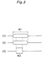
- FIG. 2(3) designates data-writing instruction signal generated by the data processor 16. While the data processor 16 retains address signal and data signal in the durable period W1, the data processor 16 generates data-writing instruction signal during a period W3 by referring to the value counted by clock circuit 18.
- the durable period W3 corresponds to 1 millisecond +/-5% for example.
- FIG. 3(1) is the waveforms of the first clock pulse output from the first clock-pulse generating circuit 20 immediately after activating power-supply source.
- the first clock-pulse reaches the threshold level value V2, and then it gradually reaches peak level V1. Accordingly, after a period W4 is past from the activation of power-supply source, arithmetic processing circuit enters into fully operative condition in which it can correctly execute normal input and output operations. This allows arithmetic processing circuit 3 to transmit and receive to and from data processor 16 of P-ROM control circuit 5 synchronous with the first clock-pulse.
- arithmetic processing circuit 3 normally outputs 8-bit data signal to data processor 16 of P-ROM control circuit 5.
- FIG. 3(2) is the waveforms of the second clock-pulse output from the second clock-pulse generating circuit 7.
- the second clock-pulse rises itself at a speed slower than that of the first clock-pulse, and thus, it reaches the threshold level value V2, after a period W5, longer than period W4, is past, and then it gradually reaches peak level V1. Accordingly, after a period W5 is past from the activation of power-supply source, data processor 16 of P-ROM control circuit 5 enters into fully operative condition in which it can correctly write data into P-ROM 6.
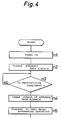
- FIG. 4 is the flowchart designating operations of the arithmetic processing circuit 3. While step n1 is underway, if power supply source were activated or power is back from interruption, then, operation mode proceeds to step n2. While step n2 is underway, if the arithmetic processing circuit 3 should write data into P-ROM 6 next for example, then, arithmetic processing circuit 3 outputs 8-bit data signal for example. While step n3 is underway, P-ROM control circuit 5 identifies whether writing of data into P-ROM 6 has already been completed, or not. If it is already completed, P-ROM control circuit 5 outputs data writing-completed signal to the arithmetic processing circuit 3.
- step n4 is which the arithmetic processing circuit 3 ceases output of all the data signals.
- step n5 is activated, in accordance with programs stored in ROM 13, the arithmetic processing circuit 3 resumes the ensuing data processing operations.
- FIG. 5 is the flowchart designating operations of the P-ROM control circuit 5 for writing data into P-ROM 6 on receipt of data from the arithmetic processing circuit 3.
- step m1 if the power-supply source turns ON or the power is again back from interruption, while step m2 is underway, then operation mode proceeds to step m2. While step m2 is underway, if data signal from the arithmetic processing circuit 3 should be written into P-ROM 6, then, operation mode enters into step m3. However, if the arithmetic processing circuit 3 outputs signals for reading data from P-ROM 6, for example, then, operation mode proceeds to step m5 in which data processing operation is executed in accordance with the output signals.
- step m3 P-ROM control circuit 5 identifies whether clock circuit 18 can count the second clock pulses, or not. If the second clock pulse were at a specific peak level higher than the threshold value level V2 (i.e., the predetermined identifying level), clock circuit 18 can count the second clock-pulse. For example, after a certain period W5 is past from the moment of activating power-supply source, clock circuit 18 can count the second clock-pulse. Data processor 16 periodically reads the value counted by clock circuit 18, and as a result, it identifies that the peak value of the second clock-pulse surpasses the threshold value level V2 by detecting variation of the value counted by clock circuit 18.
- step m4 As soon as the peak level of the second clock pulse surpasses the threshold value level V2, operation mode proceeds to step m4 to allow the data processor 16 to write data into P-ROM 6. Simultaneously, data processor 16 of P-ROM control circuit 5 outputs data-writing instruction signal based on the accurate timing W3 by calculating the value of the second clock-pulse counted by clock circuit 18. When all the needed operations designated for step m4 are terminated, operation mode returns to step m2 to cause this apparatus to repeatedly execute the same data processing operations as was done before.
- electronic cash register reflecting the preferred embodiment of the invention can freely execute all the data processing operations except for the writing of data into P-ROM 6, and thus, this electronic cash register can securely execute data-writing operation in a certain period of time shorter than the compulsory standby period needed for any conventional apparatus.
- the second clock-pulse generating circuit 7 is provided independent of the first clock-pulse generating circuit 20, which delivers the first clock pulses to other circuits, compared to the case that the second clock pulses are generated by drawing out lead wires from the first clock generating circuit 20 to write the data into P-ROM 6, it is eliminates that the fear of lowering time-basis accuracy caused by lag of time basis generated by floating capacitance. Furthermore, discretely provided second clock-pulse generating circuit 7 significantly promotes resistance against noise, thus allowing the P-ROM control circuit 5 to stably write data into P-ROM 6.
- P-ROM 6 which is substantially composed of either a bipolar P-ROM, or an EP-ROM whose content is eraseable on exposure to ultraviolet rays and whose window for receiving ultraviolet rays is molded with a beam-shielding resin, or an EEP -ROM (electrically eraseable programmable read-only memory), for example.
Landscapes
- Engineering & Computer Science (AREA)
- Computer Security & Cryptography (AREA)
- Physics & Mathematics (AREA)
- General Physics & Mathematics (AREA)
- Power Engineering (AREA)
- Read Only Memory (AREA)
- Static Random-Access Memory (AREA)
Claims (6)
- Vorrichtung (5) zum Steuern eines Festwertspeichers (6), in den Daten gemäß einem Datenschreib-Anweisungssignal hoher Genauigkeit nach dem Aktivieren einer Spannungsversorgung eingeschrieben werden, die folgendes aufweist:- eine erste Taktimpuls-Erzeugungsschaltung (7) zum Erzeugen erster Taktimpulse;- eine Einrichtung (18) zum Zählen der von der ersten Taktimpuls-Erzeugungsschaltung (7) ausgegebenen ersten Taktimpulse, wenn der Spitzenwert der ersten Taktimpulse einen vorgegebenen Schwellenwert (V₂) überschreitet, um dadurch anzuzeigen, daß der Betrieb der ersten Taktimpuls-Erzeugungsschaltung (7) stabil ist; und- eine Datenschreibeinrichtung (16) zum Erkennen, ob die erste Zähleinrichtung die ersten Taktimpulse zählen kann, und um das Datenschreib-Anweisungssignal hoher Genauigkeit an den Festwertspeicher (6) in Übereinstimmung mit den ersten Takimpulsen nur dann auszugeben, wenn der Spitzenwert der ersten Taktimpulse höher als der vorgegebene Schwellenwert (V₂) ist.
- Vorrichtung nach Anspruch 1, mit einer Einrichtung (3) zum Lesen des von der Zähleinrichtung (18) gezählten Werts in vorgegebenen Zeitintervallen, um zu erkennen, daß der Spitzenwert der ersten Takimpulse höher als der Schwellenwert ist, wenn der von der Zähleinrichtung gezählte Wert zunimmt.
- Vorrichtung nach Anspruch 1 oder Anspruch 2, bei dem der Festwertspeicher entweder einen elektrisch löschbaren, programmierbaren Festwertspeicher oder einen ultraviolettlöschbaren, programmierbaren Festwertspeicher aufweist.
- Vorrichtung nach Anspruch 3, bei der der Festwertspeicher einen ultraviolettlöschbaren, programmierbaren Festwertspeicher aufweist, dessen Fenster zum Empfangen von Ultraviolettstrahlen durch ein Strahlung abschirmendes Harz vergossen ist.
- Elektronische Registrierkasse mit:- einem Festwertspeicher (6), in den Daten abhängig von einem Datenschreib-Anweisungssignal hoher Genauigkeit eingeschrieben werden;- einer Steuervorrichtung (5) gemäß einem der vorstehenden Ansprüche, zum Steuern des Festwertspeichers;- einer Arithmetikverarbeitungseinrichtung (3) mit einer zweiten Taktimpuls-Erzeugungsschaltung (20) zum Ausführen von Arithmetikverarbeitungsvorgängen auf zweite Taktimpulse hin, wie sie von der zweiten Taktimpuls-Erzeugungsschaltung ausgegeben werden, und die die im Festwertspeicher abzuspeichernden Daten ausgibt;- wobei nach dem Aktivieren einer Spannungsversorgung (2) eine gewisse Zeitspanne verstreicht, bevor der Spitzenwert der ersten Taktimpulse den vorgegebenen Schwellenwert (V₂) übersteigt, wobei nach dem Aktivieren der Spannungsversorgung und nach der bestimmten Zeitspanne die Arithmetikverarbeitungsschaltung sicher in normale Arithmetikverarbeitungsabläufe auf die zweiten Taktimpulse hin eintritt.
- Elektronische Registrierkasse nach Anspruch 5, bei der der Festwertspeicher (6) und die Steuereinrichtung (5) zum Steuern des Festwertspeichers integral in einer einzigen Einheit ausgebildet sind, die über einen Verbinder (21) austauschbar an der Arithmetikverarbeitungseinrichtung (3) angebracht ist.
Applications Claiming Priority (2)
| Application Number | Priority Date | Filing Date | Title |
|---|---|---|---|
| JP32486087A JPH0756757B2 (ja) | 1987-12-21 | 1987-12-21 | メモリの電源投入後の制御装置 |
| JP324860/87 | 1987-12-21 |
Publications (3)
| Publication Number | Publication Date |
|---|---|
| EP0321933A2 EP0321933A2 (de) | 1989-06-28 |
| EP0321933A3 EP0321933A3 (en) | 1990-08-08 |
| EP0321933B1 true EP0321933B1 (de) | 1994-02-16 |
Family
ID=18170457
Family Applications (1)
| Application Number | Title | Priority Date | Filing Date |
|---|---|---|---|
| EP19880121330 Expired - Lifetime EP0321933B1 (de) | 1987-12-21 | 1988-12-20 | Steuereinrichtung für einen Nur-Lese-Speicher und damit ausgerüstete elektronische Kasse |
Country Status (4)
| Country | Link |
|---|---|
| EP (1) | EP0321933B1 (de) |
| JP (1) | JPH0756757B2 (de) |
| DE (1) | DE3887855T2 (de) |
| TR (1) | TR23969A (de) |
Families Citing this family (1)
| Publication number | Priority date | Publication date | Assignee | Title |
|---|---|---|---|---|
| DE102020129479B4 (de) | 2020-11-09 | 2023-11-09 | Polymath.Vision UG (haftungsbeschränkt) | Linearantrieb und Verfahren zur Linearverschiebung eines Objektes |
Family Cites Families (3)
| Publication number | Priority date | Publication date | Assignee | Title |
|---|---|---|---|---|
| JPS5840643A (ja) * | 1981-09-03 | 1983-03-09 | Toshiba Corp | 1チツプマイクロコンピユ−タの発振制御方式 |
| US4534018A (en) * | 1983-04-29 | 1985-08-06 | Pitney Bowes Inc. | Non-volatile memory protection circuit with microprocessor interaction |
| US4665328A (en) * | 1984-07-27 | 1987-05-12 | National Semiconductor Corporation | Multiple clock power down method and structure |
-
1987
- 1987-12-21 JP JP32486087A patent/JPH0756757B2/ja not_active Expired - Lifetime
-
1988
- 1988-12-20 DE DE19883887855 patent/DE3887855T2/de not_active Expired - Lifetime
- 1988-12-20 EP EP19880121330 patent/EP0321933B1/de not_active Expired - Lifetime
-
1989
- 1989-01-21 TR TR1789A patent/TR23969A/xx unknown
Also Published As
| Publication number | Publication date |
|---|---|
| EP0321933A3 (en) | 1990-08-08 |
| EP0321933A2 (de) | 1989-06-28 |
| JPH0756757B2 (ja) | 1995-06-14 |
| JPH01165094A (ja) | 1989-06-29 |
| DE3887855T2 (de) | 1994-09-01 |
| DE3887855D1 (de) | 1994-03-24 |
| TR23969A (tr) | 1991-01-11 |
Similar Documents
| Publication | Publication Date | Title |
|---|---|---|
| US5036460A (en) | Microprocessor having miswriting preventing function | |
| US6402026B1 (en) | Smart card and method for bidirectional data transfer between a terminal and a smart card | |
| EP0468454B1 (de) | Unterbrechungssteuerung | |
| US4578774A (en) | System for limiting access to non-volatile memory in electronic postage meters | |
| US5604917A (en) | IC memory card having masking function for preventing writing of data into a fixed memory area | |
| EP0092976A2 (de) | Steuergerät zur Speichereinschreibung | |
| US20010014934A1 (en) | Memory access circuit and memory access control circuit | |
| JPH05342435A (ja) | Icカード | |
| US5758121A (en) | Data storage security apparatus and method which erases memory and utilizes a power switch to cut-off electric power during unsuccessful access | |
| JPS5844823A (ja) | 電子計数回路の計数示度の記憶方法および装置 | |
| EP0173967B1 (de) | Mikroprogrammladeeinheit | |
| EP0370529A2 (de) | Mikrorechner mit EEPROM | |
| EP0197345B1 (de) | Elektronische Frankiermaschine mit Einschalt- und Ausschalt-Schutzschaltkreis | |
| EP0321933B1 (de) | Steuereinrichtung für einen Nur-Lese-Speicher und damit ausgerüstete elektronische Kasse | |
| JPH05216775A (ja) | 半導体記憶装置 | |
| EP0159530B1 (de) | Kartenleser | |
| EP0315194A2 (de) | Mikrocomputer, der fähig ist, ununterbrochen für kurze Zeit an Adressen zu gelangen | |
| CA1273713C (en) | VECTOR PROCESSING SYSTEM | |
| EP0354590A3 (de) | Befehlspufferspeicher für einen Mikrocomputer | |
| JPS58169395A (ja) | 書き替え可能なrom管理方式 | |
| US6374313B1 (en) | FIFO and method of operating same which inhibits output transitions when the last cell is read or when the FIFO is erased | |
| US5231592A (en) | Counter | |
| JPH0822422A (ja) | メモリ装置 | |
| EP0279421A2 (de) | Cachespeichersteuerungsanordnung | |
| JPH06236695A (ja) | 交換表示機能付不揮発性メモリ装置 |
Legal Events
| Date | Code | Title | Description |
|---|---|---|---|
| PUAI | Public reference made under article 153(3) epc to a published international application that has entered the european phase |
Free format text: ORIGINAL CODE: 0009012 |
|
| 17P | Request for examination filed |
Effective date: 19881220 |
|
| AK | Designated contracting states |
Kind code of ref document: A2 Designated state(s): DE GB IT |
|
| PUAL | Search report despatched |
Free format text: ORIGINAL CODE: 0009013 |
|
| AK | Designated contracting states |
Kind code of ref document: A3 Designated state(s): DE GB IT |
|
| RHK1 | Main classification (correction) |
Ipc: G11C 17/00 |
|
| 17Q | First examination report despatched |
Effective date: 19920723 |
|
| GRAA | (expected) grant |
Free format text: ORIGINAL CODE: 0009210 |
|
| AK | Designated contracting states |
Kind code of ref document: B1 Designated state(s): DE GB IT |
|
| REF | Corresponds to: |
Ref document number: 3887855 Country of ref document: DE Date of ref document: 19940324 |
|
| ITF | It: translation for a ep patent filed | ||
| PLBE | No opposition filed within time limit |
Free format text: ORIGINAL CODE: 0009261 |
|
| STAA | Information on the status of an ep patent application or granted ep patent |
Free format text: STATUS: NO OPPOSITION FILED WITHIN TIME LIMIT |
|
| 26N | No opposition filed | ||
| REG | Reference to a national code |
Ref country code: GB Ref legal event code: IF02 |
|
| PGFP | Annual fee paid to national office [announced via postgrant information from national office to epo] |
Ref country code: GB Payment date: 20071219 Year of fee payment: 20 |
|
| PGFP | Annual fee paid to national office [announced via postgrant information from national office to epo] |
Ref country code: IT Payment date: 20071228 Year of fee payment: 20 Ref country code: DE Payment date: 20071213 Year of fee payment: 20 |
|
| REG | Reference to a national code |
Ref country code: GB Ref legal event code: PE20 Expiry date: 20081219 |
|
| PG25 | Lapsed in a contracting state [announced via postgrant information from national office to epo] |
Ref country code: GB Free format text: LAPSE BECAUSE OF EXPIRATION OF PROTECTION Effective date: 20081219 |