EP0322060A2 - Filtre comportant des coefficients réglables - Google Patents
Filtre comportant des coefficients réglables Download PDFInfo
- Publication number
- EP0322060A2 EP0322060A2 EP19880202945 EP88202945A EP0322060A2 EP 0322060 A2 EP0322060 A2 EP 0322060A2 EP 19880202945 EP19880202945 EP 19880202945 EP 88202945 A EP88202945 A EP 88202945A EP 0322060 A2 EP0322060 A2 EP 0322060A2
- Authority
- EP
- European Patent Office
- Prior art keywords
- filter
- output
- stages
- signal
- coefficients
- Prior art date
- Legal status (The legal status is an assumption and is not a legal conclusion. Google has not performed a legal analysis and makes no representation as to the accuracy of the status listed.)
- Granted
Links
Images


Classifications
-
- H—ELECTRICITY
- H03—ELECTRONIC CIRCUITRY
- H03H—IMPEDANCE NETWORKS, e.g. RESONANT CIRCUITS; RESONATORS
- H03H21/00—Adaptive networks
- H03H21/0012—Digital adaptive filters
-
- H—ELECTRICITY
- H03—ELECTRONIC CIRCUITRY
- H03H—IMPEDANCE NETWORKS, e.g. RESONANT CIRCUITS; RESONATORS
- H03H17/00—Networks using digital techniques
- H03H17/02—Frequency selective networks
- H03H17/0294—Variable filters; Programmable filters
Definitions
- This invention relates to a method of adjusting the weighting coefficients corresponding to N successive stages of a transversal filter according to the least means squares algorithm, in which method signal samples are supplied to the filter in succession, differences between output signals of the filter and a reference are determined, which output signals each result from a respective group of N of said samples being weighted by said weighting coefficients, and a respective correction derived from the product of a said difference and the current content of a stage of the filter is applied to each said weighting coefficient.
- the invention also relates to a modification of such a method in which inter alia the transversal filter is replaced by a decision feedback filter. Moreover the invention relates to arrangements for implementing such methods.
- weighting coefficients of a transversal filter be adjusted in order to render the filter characteristic closer to that currently required.
- a filter may be employed as a so-called “equaliser” for compensating for distortion to a transmitted signal caused by the imperfect nature of a transmission channel. If the channel characteristics vary with time then, in order that satisfactory equalisation continues to be achieved, it is necessary that the filter characteristic be updated either effectively continuously or periodically to take into account the changed channel characteristics.
- the "least mean squares algorithm” being one of several algorithms which could be employed for the adjustment process.
- C N (k) are the weighting coefficients corresponding to the N successive stages of the filter for a given sample period k of the input signal
- ⁇ is a constant which is usually less than 0.1
- e(k) is the difference between the output of the filter and the reference for the given sample period k
- V1(k), V2(k), ... V N (k) are the respective contents of the N successive stages of the filter for the given sample period k.
- a method as defined in the first paragraph is characterised in that the filter includes at least one further stage which succeeds the N successive stages and the weighting coefficient corresponding to which is set to zero for the production of each said output signal, in that each of the N coefficients is adjusted only once for each n samples applied to the filter, where n is greater than unity, and in that each correction is derived from the output of the filter after the entering of values representative of a plurality of said differences into the filter as respective weighting coefficients and the setting of any remaining weighting coefficients to zero.
- V1(k-1) V2(k) so that the only quantity which needs to be saved is e(k-1).
- the filter itself can be made to evaluate the quantity inside the square brackets above by the simple expedient of substituting the quantities e(k) and e(k-1) for the weighting coefficients C1 and C2 respectively, and setting any other weighting coefficients to zero.
- the filter were to have exactly N stages, although the quantity V N (k) would be present in the filter for the sample period k, the quantities V N (k-1), V N (k-2) etc. will have dropped out of the end.
- the filter will have to be provided with at least n-1 further stages succeeding the N stages so that the quantities V N (k-1) ...V N (k-(n-1)) do not drop out until they are no longer needed.
- the quantity [e(k)V N (k) + e(k-1) V N (k-1) + ... + e(k-(n-1)) V N (k-(n-1))] may be evaluated by means of the filter in a similar way to that set forth above, i.e.
- n N and one correction for a coefficient is derived for each sample applied to the filter.
- the aforesaid one aspect of the present invention can be employed to adjust the weighting coefficients of a so-called "decision feedback" filter if it is arranged that the input signals to the filter are in multiplexed form. More specifically, it may be arranged that a respective said output signal is produced for each pair of signal samples applied to the filter and that alternate ones of said signal samples are derived from a said output signal via a decision element, and from an external signal source respectively.
- the invention provides a method of adjusting the weighting coefficients corresponding to N stages of a decision feedback filter arrangement according to the least mean squares algorithm, said filter arrangement comprising first and second transversal filters having a common output which is coupled to the input of the second filter via a decision element, X successive stages of the first filter and Y successive stages of the second filter together constituting said N stages, in which method signal samples are supplied to the first filter in succession, differences between output signals appearing at said common output and corresponding signals appearing at the decision element output are determined, and a respective correction derived from the product of a said difference and the current content of a stage of a said filter is applied to each said weighting coefficient, each said output signal appearing at said common output resulting from a respective group of X of said samples and Y of the signals derived from the decision element output which are applied to the second filter being weighted by said weighting coefficients, characterised in that the first filter includes at least one further stage which succeeds said X successive stage and the second filter includes at least one further stage which succeed
- the invention also provides transversal and decision feedback filter arrangements for implementing the aspects of the invention defined above.
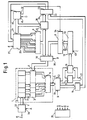
- a transversal filter arrangement comprises a conventional transversal filter 1 in the form of a delay line or shift register 2 having (N+n-1) stages, a multiplier array 3 comprising a respective multiplier corresponding to each stage of the register 2, and an adder 4 which adds together the outputs of all the multipliers of the array 3 and produces the result on an output 5.
- Each multiplier of the array 3 has a first input coupled to an output of the corresponding stage of the register 2 and a second input fed from a respective group of bit-lines of a multiple input 6 and multiplies the content of the corresponding stage of the register 2 by a (digital) quantity applied in operation to the respective group of bit lines of the input 6.
- the serial input 7 of the shift register 2 is also multibit, as is the storage capacity of each stage of the register 2.
- the input 6 is fed from the parallel outputs of a first auxiliary register 8 and a second auxiliary register 9 as alternatives via a two-position multiplexer 10.
- Each of the registers 9 and 10 contains a multibit storage stage corresponding to each multiplier of the array 3 and, when the multiplexer connects the parallel output of the relevant register 9 or 10 to the input 6, the content of each stage is applied to the bit lines of the input 6 which feed the corresponding multiplier.
- the contents of the stages of the register 2 are weighted by the contents of the corresponding stages of the register 8 or 9 and the results are added together by the adder 4.
- the input 7 of the (clocked) shift register 2 is fed from an input terminal 11 via a correspondingly clocked sampling analog-to-digital converter 12.
- Input terminal 11 is connected to the output of an external signal source (not shown).
- Input 7 is therefore fed with a succession of samples V in digital form of an analogue input signal applied to terminal 11, these samples being clocked through the register 2 in succession and giving rise to corresponding filtered signal samples in digital form at the the output 5.
- Output 5 is connected, via a two position demultiplexer 12, as alternatives to either the input of a multiplier 14 or to both the input of a decision element 15 and a first input of a subtractor 16.
- the output of decision element 15 feeds both an output 17 and also the second input of the subtrctor 16.
- decision element 15 takes, on the basis of the potentially distorted signals fed to its input from the output 5, decisions on what these signals would ideally be in the absence of such distortion and produces the results of these decisions on its output, whence they are fed to the output 17.
- the decisions may be taken, for example, on the basis of a reference to all the possible values which the output signals of converter 12 could have in the absence of distortion or, as another example, on the basis of a reference to the undistorted form of a standard signal a potentially distorted version of which is periodically received on the input terminal 11.
- the difference e between the successive output signals of decision element 15 and the corresponding signals appearing at the output 5 of filter 1 are calculated by subtractor 16 and are clocked in succession into a shift register 18 via its serial input 19.
- Shift register 18 has n stages, and its parallel output 20 is connected to the parallel input 1 of the right-hand n stages of register 8, the remaining N-1 left-hand stages of register 8 being loaded with zeros on a permanent basis.
- the right-hand n stages of register 8 correspond to the n multipliers at the right-hand end of array 3.
- Multiplier 14 multiplies the signals fed to it from the filter output 5 by a fixed constant value ⁇ , and applies the result to one input 22 of an adder 23.
- the other input 24 of adder 23 is fed with the contents of a selected one of the N left-hand stages of register 9 via an N-position multiplexer 25, these N left-hand stages corresponding to the N multipliers at the left-hand end of the array 3 (which contains N+n-1 multipliers in all).
- the remaining stages of register 9 are loaded with zeros on a permanant basis.
- the output of adder 23 is fed to the input of a selected one of the N left-hand stages of register 9 via an N-position demultiplexer 26, the stages selected by (de)multiplexers 25 and 26 at any given time being the same.
- Each of the said N left-hand stages also has a respective load signal input (not shown), and that stage which is at any given time selected by demultiplexer 26 also has its load signal input connected through demultiplexer 26 to a further bit input 27 of demultiplexer 26.
- Control or selection signal inputs 28 and 29 of the (de)multiplexers 25 and 26 respectively are fed from the output 30 of a counter 31 which has a capacity N.
- a "borrow" signal output 32 of counter 31 is connected to a parallel load input 34 of register 8.
- Register 8 is therefore loaded each time (decremented) counter 31 is changed to a state in which it controls (de)multiplexers 25 and 26 to select the Nth stage of register 9.
- the components 2, 10, 12, 13, 18 and 31 are supplied with clock/control signals from outputs A, B, C, D and E of a clock/control signal generator 35 as shown.
- the time relationship between these signals is indicated in Figure 2 of the drawings.
- Signal A is applied to a sampling control signal input 36 of analog-to-digital converter 12 and to a clock signal input 37 of delay line or shift register 2, so that each time a rising edge occurs in the signal A, a sample is taken of a signal applied to input 11, is converted to digital form, and is clocked into the first stage of register 2.
- Signal B is applied to select signal inputs 38 and 39 of the (de)multiplexers 10 and 13.
- a high level in this signal causes multiplexer 10 to connect the parallel output of register 9 to input 6 and demultiplexer 13 to connect output 5 to decision device 15 and subtractor 16, these (de)multiplexers taking up their other selection state when signal B is low.
- Signal C is supplied to the clock signal input 40 of shift register 18 so that the output of subtractor 16 is loaded into the first stage of register 18 each time a rising edge occurs in signal C.
- Signal D is applied to the clock signal input 41 of (cyclic) counter 31, so that the content of counter 31 is decremented on each rising edge of signal D.
- Signal E is applied to the bit line input 27 of demultiplexer 26 so that the stage of register 9 currently selected by demultiplexer 26 is loaded with the output of adder 23 each time a rising edge occurs in the signal E.
- the contents e of register 8 are used for the filter weighting coefficients (only the samples in the last n stages at most of register 2 contributing to the resulting signal applied to multiplier 14 because the contents of the stages of register 8 which correspond to the remaining stages of register 2 are permanently zero).
- the resulting output of multiplier 14 is used to correct, under the control of signal E, the weighting coefficient contained in that stage of register 9 which is currently being selected by (de)multiplexers 25 and 26 under the control of counter 31.
- the output of multiplier 14 is ⁇ [e(k) V1(k-2) + e(k-1) V1(k-3) + e(k-2) V1(k-4)], i.e. the required correction for the weighting coefficient C3 for the third stage of the register.
- the outputs from multiplier 14 are the required corrections for the weighting coefficients for the second (C2), first (C1) and third (C3) stages of register 2, as required.
- an integrated circuit having an architecture corresponding to the combination of the items 1, 8, 9 and 10 is commercially available from Inmos under the type number A100, and such an integrated circuit may be used to implement these components. If this is done the arrangement of the clock/control signal generator 35, (de)multiplexers 25 and 26, and counter 31 will have to be modified somewhat to take into account that with this integrated circuit the various stages of the registers 8 and 9 have to be accessed by applying appropriate address signals to the circuit.
- one of the N coefficients in register 9 is adjusted for each sample period of the signal applied to input 11.
- more than one coefficient may be adjusted for each said period, enabling the excess of the number of stages of register 2 over N to be reduced while still taking into account the maximum amount of information for the adjustment of each coefficient, albeit at the expense of having to carry out more operations during each sample period.
- the error signal e(k) After the error signal e(k) has been derived from the output of the filter it is used as the weighting coefficient for the fourth stage of register 2 and e(k-1) is used as the weighting coefficient for the fifth stage.
- the output of multiplier 14 is therefore ⁇ [e(k) V1(k-3) + e(k-1) V(k-4)], i.e. the required correction for weighting coefficient C4 for the fourth stage of register 2.
- the error signals e(k) and e(k-1) are now used, still during the sample period k , as weighting coefficients for the third and fourth stages of register 2 respectively resulting in the required correction for the weighting coefficient C3 for the third stage of register 2.
- each weighting coefficient C immediately the required correction therefor has been calculated, in order to minimise the settling time of the filter.
- a plurality of coefficients is adjusted every m sample periods, where m is greater than one.
- the embodiment of Figure 1 could be modified so that all the N coefficients in register 9 are adjusted as a group each time the contents of register 18 are written into register 8.
- the filter 1 of Figure 1 together with items 8-10, 13, 14, 23, 25, 27 and 31 and their interconnections may be duplicated, the duplicate of filter 1 forming the feedback element of the filter arrangement. More specifically, the input 7 of the duplicate of filter 1 may be fed from the output 17 via a sign reverser, and the signal path from one input to the output of a further adder (not shown) may be included between the output 5 and demulitplexer 13 in Figure 1.
- the counters 31 and its duplicate are in such a case arranged to run in step, so that their contents are always equal to each other; these counters could be replaced by a single common counter if desired. Because of the provision of the sign reverser, during the first half of each input signal sample period the appropriately weighted N previous signals I at output 17 are now subtracted in the further adder from the suitably weighted N most recent input signal samples now present in register 2, and the result is applied to decision element 15 and subtractor 15 via multiplexer 13 as required.
- the decision feedback filter arrangement described above may be modified so that only a single transversal filter 1 is employed, albeit of double length and albeit at the expense of having to increase the lengths of registers 8 and 9 and to carry out more operations serially during each input signal sample period.
- a single transversal filter 1 instead of connecting the output 17 of Figure 1 to a duplicate of filter 1 via a sign reverser it may be connected, via the sign reverser and one input and the output of a multiplexer, to the input 7 of filter 1, the output of the analog-to-digital converter being connected to the other input of this multiplexer.
Landscapes
- Physics & Mathematics (AREA)
- Engineering & Computer Science (AREA)
- Computer Hardware Design (AREA)
- Mathematical Physics (AREA)
- Filters That Use Time-Delay Elements (AREA)
- Cable Transmission Systems, Equalization Of Radio And Reduction Of Echo (AREA)
Applications Claiming Priority (2)
| Application Number | Priority Date | Filing Date | Title |
|---|---|---|---|
| GB8729988 | 1987-12-23 | ||
| GB8729988A GB2214035A (en) | 1987-12-23 | 1987-12-23 | Adjusting filter coefficients |
Publications (3)
| Publication Number | Publication Date |
|---|---|
| EP0322060A2 true EP0322060A2 (fr) | 1989-06-28 |
| EP0322060A3 EP0322060A3 (en) | 1990-10-24 |
| EP0322060B1 EP0322060B1 (fr) | 1995-10-11 |
Family
ID=10628942
Family Applications (1)
| Application Number | Title | Priority Date | Filing Date |
|---|---|---|---|
| EP19880202945 Expired - Lifetime EP0322060B1 (fr) | 1987-12-23 | 1988-12-19 | Filtre comportant des coefficients réglables |
Country Status (4)
| Country | Link |
|---|---|
| EP (1) | EP0322060B1 (fr) |
| JP (1) | JP2865681B2 (fr) |
| DE (1) | DE3854572T2 (fr) |
| GB (1) | GB2214035A (fr) |
Cited By (4)
| Publication number | Priority date | Publication date | Assignee | Title |
|---|---|---|---|---|
| EP0421962A1 (fr) * | 1989-10-04 | 1991-04-10 | Telefonaktiebolaget L M Ericsson | Procédé et dispositif pour une division arithmétique approximative |
| EP0735674A3 (fr) * | 1995-03-30 | 1997-09-17 | At & T Corp | Procédé et dispositif pour le filtrage adaptatif |
| EP0804768A4 (fr) * | 1994-12-28 | 2000-07-26 | Quantum Corp | Circuit a faible consommation d'adaptation des coefficients de filtre du type filtre adaptatif numerique |
| WO2001001570A1 (fr) * | 1999-06-25 | 2001-01-04 | Infineon Technologies Ag | Filtre passe-bande programmable pour un circuit codec |
Family Cites Families (3)
| Publication number | Priority date | Publication date | Assignee | Title |
|---|---|---|---|---|
| US4038536A (en) * | 1976-03-29 | 1977-07-26 | Rockwell International Corporation | Adaptive recursive least mean square error filter |
| DE2724561C2 (de) * | 1977-05-31 | 1983-09-29 | Siemens AG, 1000 Berlin und 8000 München | Adaptiver Entzerrer für breitbandige Signale |
| US4644562A (en) * | 1985-08-28 | 1987-02-17 | At&T Company | Combined cross polarization interference cancellation and intersymbol interference equalization for terrestrial digital radio systems |
-
1987
- 1987-12-23 GB GB8729988A patent/GB2214035A/en not_active Withdrawn
-
1988
- 1988-12-19 DE DE19883854572 patent/DE3854572T2/de not_active Expired - Fee Related
- 1988-12-19 EP EP19880202945 patent/EP0322060B1/fr not_active Expired - Lifetime
- 1988-12-20 JP JP63321842A patent/JP2865681B2/ja not_active Expired - Lifetime
Cited By (8)
| Publication number | Priority date | Publication date | Assignee | Title |
|---|---|---|---|---|
| EP0421962A1 (fr) * | 1989-10-04 | 1991-04-10 | Telefonaktiebolaget L M Ericsson | Procédé et dispositif pour une division arithmétique approximative |
| WO1991005305A1 (fr) * | 1989-10-04 | 1991-04-18 | Telefonaktiebolaget Lm Ericsson | Procede et dispositif permettant d'effectuer une division arithmetique approximative |
| US5303177A (en) * | 1989-10-04 | 1994-04-12 | Telefonaktiebolaget L M Ericsson | Method and device for performing an approximate arithmetical division |
| US5325319A (en) * | 1989-10-04 | 1994-06-28 | Telefonaktiebolaget L M Ericsson | Filtering a signal with the use of approximate arithmetical division |
| EP0804768A4 (fr) * | 1994-12-28 | 2000-07-26 | Quantum Corp | Circuit a faible consommation d'adaptation des coefficients de filtre du type filtre adaptatif numerique |
| EP0735674A3 (fr) * | 1995-03-30 | 1997-09-17 | At & T Corp | Procédé et dispositif pour le filtrage adaptatif |
| WO2001001570A1 (fr) * | 1999-06-25 | 2001-01-04 | Infineon Technologies Ag | Filtre passe-bande programmable pour un circuit codec |
| US7639744B1 (en) | 1999-06-25 | 2009-12-29 | Infineon Technologies Ag | Programmable digital bandpass filter for a codec circuit |
Also Published As
| Publication number | Publication date |
|---|---|
| GB2214035A (en) | 1989-08-23 |
| DE3854572D1 (de) | 1995-11-16 |
| DE3854572T2 (de) | 1996-06-27 |
| JP2865681B2 (ja) | 1999-03-08 |
| EP0322060B1 (fr) | 1995-10-11 |
| JPH01202008A (ja) | 1989-08-15 |
| EP0322060A3 (en) | 1990-10-24 |
| GB8729988D0 (en) | 1988-02-03 |
Similar Documents
| Publication | Publication Date | Title |
|---|---|---|
| US5416799A (en) | Dynamically adaptive equalizer system and method | |
| US6035320A (en) | Fir filter architecture | |
| US4982354A (en) | Digital finite impulse response filter and method | |
| US4843583A (en) | Nonlinear adaptive filter | |
| US5555200A (en) | Charge domain bit-serial multiplying digital-analog converter | |
| DE69229704T2 (de) | Vorrichtung und verfahren zur asynchronen zyklischen redundanzprüfung in digitalen empfängern | |
| CA1116702A (fr) | Filtre digital recursif | |
| US6032171A (en) | Fir filter architecture with precise timing acquisition | |
| US5831879A (en) | Digital transmit filter | |
| US4611305A (en) | Digital signal processing circuit | |
| US5216629A (en) | Adjusting filter coefficients | |
| US4817025A (en) | Digital filter | |
| US5440503A (en) | Digital filtering circuit operable as a three-stage moving average filter | |
| US4580128A (en) | Digital signal processing device | |
| US5381354A (en) | Digital filtering of blocks of data values with symmetric data extension at edges of the blocks | |
| US5506798A (en) | Digital filter and oversampling analog to digital converter employing the same | |
| EP0322060B1 (fr) | Filtre comportant des coefficients réglables | |
| JPS63174419A (ja) | デジタル信号補償装置 | |
| DE69415561T2 (de) | Transversaler Filter geeignet zur Verarbeitung von Eingangssignalen mit hoher Datenrate | |
| US4893264A (en) | Digital decimation filter | |
| EP0566246B1 (fr) | Filtre numérique | |
| US5097433A (en) | Stack filter with one stage per bit | |
| US5901175A (en) | Dynamically adaptive equalizer system and method | |
| US5233549A (en) | Reduced quantization error FIR filter | |
| US5333263A (en) | Digital image processing apparatus |
Legal Events
| Date | Code | Title | Description |
|---|---|---|---|
| PUAI | Public reference made under article 153(3) epc to a published international application that has entered the european phase |
Free format text: ORIGINAL CODE: 0009012 |
|
| AK | Designated contracting states |
Kind code of ref document: A2 Designated state(s): DE FR GB IT |
|
| PUAL | Search report despatched |
Free format text: ORIGINAL CODE: 0009013 |
|
| AK | Designated contracting states |
Kind code of ref document: A3 Designated state(s): DE FR GB IT |
|
| 17P | Request for examination filed |
Effective date: 19910418 |
|
| RAP3 | Party data changed (applicant data changed or rights of an application transferred) |
Owner name: N.V. PHILIPS' GLOEILAMPENFABRIEKEN Owner name: PHILIPS ELECTRONICS UK LIMITED |
|
| 17Q | First examination report despatched |
Effective date: 19930701 |
|
| GRAA | (expected) grant |
Free format text: ORIGINAL CODE: 0009210 |
|
| AK | Designated contracting states |
Kind code of ref document: B1 Designated state(s): DE FR GB IT |
|
| REF | Corresponds to: |
Ref document number: 3854572 Country of ref document: DE Date of ref document: 19951116 |
|
| ITF | It: translation for a ep patent filed | ||
| ET | Fr: translation filed | ||
| PLBE | No opposition filed within time limit |
Free format text: ORIGINAL CODE: 0009261 |
|
| STAA | Information on the status of an ep patent application or granted ep patent |
Free format text: STATUS: NO OPPOSITION FILED WITHIN TIME LIMIT |
|
| 26N | No opposition filed | ||
| REG | Reference to a national code |
Ref country code: FR Ref legal event code: CD |
|
| PGFP | Annual fee paid to national office [announced via postgrant information from national office to epo] |
Ref country code: GB Payment date: 20001220 Year of fee payment: 13 |
|
| PGFP | Annual fee paid to national office [announced via postgrant information from national office to epo] |
Ref country code: FR Payment date: 20001226 Year of fee payment: 13 |
|
| PGFP | Annual fee paid to national office [announced via postgrant information from national office to epo] |
Ref country code: DE Payment date: 20010214 Year of fee payment: 13 |
|
| PG25 | Lapsed in a contracting state [announced via postgrant information from national office to epo] |
Ref country code: GB Free format text: LAPSE BECAUSE OF NON-PAYMENT OF DUE FEES Effective date: 20011219 |
|
| REG | Reference to a national code |
Ref country code: GB Ref legal event code: IF02 |
|
| PG25 | Lapsed in a contracting state [announced via postgrant information from national office to epo] |
Ref country code: DE Free format text: LAPSE BECAUSE OF NON-PAYMENT OF DUE FEES Effective date: 20020702 |
|
| GBPC | Gb: european patent ceased through non-payment of renewal fee |
Effective date: 20011219 |
|
| PG25 | Lapsed in a contracting state [announced via postgrant information from national office to epo] |
Ref country code: FR Free format text: LAPSE BECAUSE OF NON-PAYMENT OF DUE FEES Effective date: 20020830 |
|
| REG | Reference to a national code |
Ref country code: FR Ref legal event code: ST |
|
| PG25 | Lapsed in a contracting state [announced via postgrant information from national office to epo] |
Ref country code: IT Free format text: LAPSE BECAUSE OF NON-PAYMENT OF DUE FEES;WARNING: LAPSES OF ITALIAN PATENTS WITH EFFECTIVE DATE BEFORE 2007 MAY HAVE OCCURRED AT ANY TIME BEFORE 2007. THE CORRECT EFFECTIVE DATE MAY BE DIFFERENT FROM THE ONE RECORDED. Effective date: 20051219 |