EP0421962A1 - Procédé et dispositif pour une division arithmétique approximative - Google Patents
Procédé et dispositif pour une division arithmétique approximative Download PDFInfo
- Publication number
- EP0421962A1 EP0421962A1 EP90850300A EP90850300A EP0421962A1 EP 0421962 A1 EP0421962 A1 EP 0421962A1 EP 90850300 A EP90850300 A EP 90850300A EP 90850300 A EP90850300 A EP 90850300A EP 0421962 A1 EP0421962 A1 EP 0421962A1
- Authority
- EP
- European Patent Office
- Prior art keywords
- bits
- logic
- binary
- represent
- character
- Prior art date
- Legal status (The legal status is an assumption and is not a legal conclusion. Google has not performed a legal analysis and makes no representation as to the accuracy of the status listed.)
- Granted
Links
Images

Classifications
-
- G—PHYSICS
- G06—COMPUTING OR CALCULATING; COUNTING
- G06F—ELECTRIC DIGITAL DATA PROCESSING
- G06F7/00—Methods or arrangements for processing data by operating upon the order or content of the data handled
- G06F7/38—Methods or arrangements for performing computations using exclusively denominational number representation, e.g. using binary, ternary, decimal representation
- G06F7/48—Methods or arrangements for performing computations using exclusively denominational number representation, e.g. using binary, ternary, decimal representation using non-contact-making devices, e.g. tube, solid state device; using unspecified devices
- G06F7/52—Multiplying; Dividing
- G06F7/535—Dividing only
-
- H—ELECTRICITY
- H03—ELECTRONIC CIRCUITRY
- H03H—IMPEDANCE NETWORKS, e.g. RESONANT CIRCUITS; RESONATORS
- H03H21/00—Adaptive networks
- H03H21/0012—Digital adaptive filters
Definitions
- the present invention relates to a method of performing an approximate arithmetical division of a constant number by a variable number in binary form when updating an adaptive digital filter, the value of the variable number representing the signal energy of an input signal to the filter and existing in the form of electric signals which represent logic ones and logic zeroes, said variable number including a character bit, N1 whole-number bits and N2 binary fraction bits, where N1 ⁇ 0 and N2 ⁇ 0.
- the invention also relates to an arrangement for performing an approximate division of a constant number by a number in binary form which includes a character bit, N1 whole-number bits and N2 binary fraction bits, where N1 ⁇ 0 and N2 ⁇ 0, comprising a first input for obtaining said character bit, N1+N2 inputs for obtaining said whole-number bits and binary fraction bits, a first output for handling a character bit and N1+N2 outputs for handling wholenumber bits and binary fraction bits.
- an aritmethical division operation is performed as a series of repeated so-called conditional subtractions.
- the absolute accuracy obtained herewith is proportional to the number of iterations.
- Arithmethical division operations can also be performed with the aid of equipment that has a relatively large memory capacity.
- One example in this regard is found described in US 4,707,798, according to which an approximate arithmethical division is effected by so-called table look-up in a memory in combination with interpolation.
- One object of the present invention is to provide a method which will enable an arithmetical division of the kind mentioned in the introduction to be carried out rapidly and with the aid of simple equipment. This is achieved in two stages. There is first formed a digital word, by substituting with logic zeroes any logic ones which have a lower significance than the most significant logic one of the bits which give the absolute value of the variable number. There is then formed in binary form a new number which has similar character bits to the variable number, and the bits in the digital word are read in the reverse sequence.
- Another object of the invention is to provide an arrangement of the aforesaid kind of simple construction which will enable an approximate division to be carried out rapidly.
- the device comprises essentially only one logic device which functions to substitute with logic zeroes any logic ones that have a lower significance than the most significant logic one.
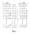
- Figures 1 and 2 are tables illustrating examples of the relationship between mutually different input values and output values in binary form when performing an inventive division operation, and also different digital words which are constructed as a link in such a division
- Figure 3 illustrates a gate network which constitutes an example of an arrangement for carrying out an inventive division operation.
- the column furthest to the left in the table shows examples of different numbers in binary form whose values vary between zero and 15/16.
- the first bit in each number is a character bit and has zero value, which in the case of the illustrated example signifies that the number is positive.
- the point following the first zero is a so-called binary point and indicates that the subsequent bits have the values 1/2, 1/4, 1/8 and 1/16, as will also be seen from the Figure.
- the illustrated binary numbers do not include a whole-number bit, but comprise solely one character bit and four so-called binary fraction bits.
- a digital word is formed from the binary fraction bits in a first stage of the process, i.e. from the four bits to the right of the character bit in the binary number.
- Different digital words of this kind are shown in the centre column of the Figure. Each of these words is formed by substituting with logic zeroes any logic ones which have a lower significance than the most significant logic one in the binary number.
- Each such digital word will thus consist of a single logic one and three logic zeroes, with the exception of the lowermost word in the table, which corresponds to the binary number zero and which consists of four logic zeroes.
- a new number is formed in binary form in a second stage, and the right-hand column of the Figure illustrates different number thus formed.
- Each of the new numbers has a character bit similar to corresponding numbers in the left-hand column, and the binary point is located in the same position as in the corresponding number.
- the binary bits which follow the binary point coincides with the bits in corresponding digital words in the centre column, but are read in the reverse order.
- division with zero is not a defined operation, the division of the number zero can, in principle, be arbitrarily selected. In the present case, it has been considered appropriate for the number zero to result in the number zero subsequent to division. This is because when the division process is applied in conjunction with adjustment to the settings of adaptive filters, it is probable that the number zero on the converter input originates from a momentarily "silent" transmission channel. This shall not result in an adjustment or change to the filter setting.
- Figure 2 illustrates a second table that contains various numbers in binary form. These numbers coincide with the numbers in the table of Figure 1, but with the binary point having been moved two places to the right. The numbers therefore have two whole-number bits having the values 2 and 1, and two binary fraction bits having the values 1/2 and 1/4, which are marked in the Figure.
- the numbers are converted according to the same principle as that applied with the numbers shown in Figure 1, and the digital words in the centre column therefore coincide exactly with corresponding words in Figure 1.
- the converted numbers in the right-hand column include two binary bits to the right of the binary point, i.e. two binary fraction bits.
- the arithmetic division of binary numbers which have solely a single logic one corresponds to the division of 1/2 by the number concerned. For instance, 1/4 is converted to 2.
- the number 3 3/4 is written in binary form as 011.11 and is converted to 1/4. This corresponds to a division of the number (30/16)x1/2, i.e. almost 2x1/2, by the number 3 3/4.
- the division method will thus correspond to an approximate division of a constant number whose value lies roughly centrally between 1/2 and 1, and the binary number concerned.
- the number zero is an exception, since this number is not changed at all.
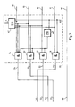
- FIG 3 illustrates an exemplifying embodiment of an arrangement for carrying out an approximate division in accordance with the aforegoing.
- the arrangement has five inputs 10-14 and five outputs 50-54.
- the input 10 is connected to the output 50 and is intended to be supplied with the character bit of a binary input number.
- the character bit is thus transmitted unchanged from the input 10 to the output 50.
- the most significant bit, the next most significant bit and so on of the input number are applied to the inputs 11-14 in that sequence.
- the inputs 11-14 are connected to a logic device 20 having outputs 21-24.
- the logic device 20 will be described in more detail hereinafter, and functions to find the most significant logic one on the inputs 11-14 and to substitute with logic zeroes any logic ones of lower significance.
- the digital words shown in the centre columns in Figures 1 and 2 are thus handled on the outputs 21-24.
- the outputs 21-24 from the device 20 are connected to the outputs 51-54 of said device, by coupling the output 21 to the output 54, the output 22 to the output 53, and so on. In this way, the bits in the digital word from the device 20 will occur in a reversed order on the outputs 51-54 of said device.
- the character bit on the output 50 and the bits on the output 51-54 thus form the binary words shown in the respective right-hand columns of Figures 1 and 2.
- the device 20 comprises a gate network which includes four AND-gates 31-34 and two OR-gates 41-42 and is intended to convert binary numbers which have four binary bits in addition to the character bits.
- An input 15 and an output 25 are intended for so-called carry bits which are used when several gate networks of the illustrated kind are connected in cascade. This makes it possible to convert binary numbers comprising more than four bits. If the gate network is not cascade-connected to a similar network for bits of higher significance than the bit on the input 11, a logic zero is sent to the carry input 15.
- a logic zero on the carry input 15 will hold the gate 31 open for a possible logic one on the input 11 for the most significant bit in a binary number supplied to the network. If the most significant bit is a logic one, a logic one will therefore also appear on the output 21 of the gate 31. The presence of a logic one on the input 11 will also result in the presence of a logic zero on a negated output of the gate 41, and this logic zero will latch the gates 32-34 so that logic zeroes occur on the outputs 22-24 irrespective of whether logic ones or logic zeroes appear on the inputs 12-14. If the most significant bit is, instead, a logic zero, a logic zero will also appear on the output 21 and a logic one will appear on the output of the gate 41.
- This logic one holds the gate 32 open for a possible logic one on the input 12 for the next most significant bit of the binary number.
- a logic one on the input 12 will, at the same time, latch the gates 33 and 34, so that logic zeroes will appear on the outputs 23 and 24.
Landscapes
- General Physics & Mathematics (AREA)
- Engineering & Computer Science (AREA)
- Physics & Mathematics (AREA)
- Computational Mathematics (AREA)
- Mathematical Analysis (AREA)
- Mathematical Optimization (AREA)
- Pure & Applied Mathematics (AREA)
- Theoretical Computer Science (AREA)
- Computing Systems (AREA)
- General Engineering & Computer Science (AREA)
- Compression, Expansion, Code Conversion, And Decoders (AREA)
- Image Processing (AREA)
- Resistance Heating (AREA)
- Led Devices (AREA)
- Filters That Use Time-Delay Elements (AREA)
- Cable Transmission Systems, Equalization Of Radio And Reduction Of Echo (AREA)
- Magnetic Heads (AREA)
- Paper (AREA)
- Analysing Materials By The Use Of Radiation (AREA)
- Prostheses (AREA)
- Complex Calculations (AREA)
Applications Claiming Priority (2)
| Application Number | Priority Date | Filing Date | Title |
|---|---|---|---|
| SE8903265A SE464787B (sv) | 1989-10-04 | 1989-10-04 | Foerfarande och anordning foer att utfoera en approximativ division |
| SE8903265 | 1989-10-04 |
Publications (2)
| Publication Number | Publication Date |
|---|---|
| EP0421962A1 true EP0421962A1 (fr) | 1991-04-10 |
| EP0421962B1 EP0421962B1 (fr) | 1995-11-22 |
Family
ID=20377054
Family Applications (1)
| Application Number | Title | Priority Date | Filing Date |
|---|---|---|---|
| EP90850300A Expired - Lifetime EP0421962B1 (fr) | 1989-10-04 | 1990-09-10 | Procédé et dispositif pour une division arithmétique approximative |
Country Status (16)
| Country | Link |
|---|---|
| US (2) | US5303177A (fr) |
| EP (1) | EP0421962B1 (fr) |
| JP (1) | JP3164363B2 (fr) |
| KR (1) | KR0121945B1 (fr) |
| AU (1) | AU630752B2 (fr) |
| BR (1) | BR9006933A (fr) |
| CA (1) | CA2042028C (fr) |
| DE (1) | DE69023735T2 (fr) |
| DK (1) | DK0421962T3 (fr) |
| ES (1) | ES2081362T3 (fr) |
| FI (1) | FI98101C (fr) |
| GR (1) | GR3018200T3 (fr) |
| IE (1) | IE70324B1 (fr) |
| NO (1) | NO178088C (fr) |
| SE (1) | SE464787B (fr) |
| WO (1) | WO1991005305A1 (fr) |
Cited By (1)
| Publication number | Priority date | Publication date | Assignee | Title |
|---|---|---|---|---|
| WO1998007102A3 (fr) * | 1996-08-08 | 1998-06-11 | Northern Telecom Ltd | Elimination de la division dans un algorithme a moyenne quadratique minimale normalisee |
Families Citing this family (1)
| Publication number | Priority date | Publication date | Assignee | Title |
|---|---|---|---|---|
| US5589832A (en) * | 1994-12-02 | 1996-12-31 | Lucent Technologies Inc. | Low noise non-sampled successive approximation |
Citations (6)
| Publication number | Priority date | Publication date | Assignee | Title |
|---|---|---|---|---|
| US4607343A (en) * | 1982-12-23 | 1986-08-19 | International Business Machines Corp. | Apparatus and method for performing division with an extended range of variables |
| US4707798A (en) * | 1983-12-30 | 1987-11-17 | Hitachi, Ltd. | Method and apparatus for division using interpolation approximation |
| US4726036A (en) * | 1987-03-26 | 1988-02-16 | Unisys Corporation | Digital adaptive filter for a high throughput digital adaptive processor |
| EP0322060A2 (fr) * | 1987-12-23 | 1989-06-28 | Philips Electronics Uk Limited | Filtre comportant des coefficients réglables |
| US4872184A (en) * | 1987-07-21 | 1989-10-03 | Nec Corporation | Digital automatic line equalizer with means for controlling tap gains of transversal filter based on mean power of output from the filter |
| EP0345675A2 (fr) * | 1988-06-09 | 1989-12-13 | National Semiconductor Corporation | Algorithme hybride stochastique du gradient pour la convergence de filters adaptatifs |
Family Cites Families (4)
| Publication number | Priority date | Publication date | Assignee | Title |
|---|---|---|---|---|
| US4181976A (en) * | 1978-10-10 | 1980-01-01 | Raytheon Company | Bit reversing apparatus |
| JPS62118474A (ja) * | 1985-11-19 | 1987-05-29 | Hitachi Ltd | ベクトル除算装置の制御方式 |
| US4782457A (en) * | 1986-08-18 | 1988-11-01 | Texas Instruments Incorporated | Barrel shifter using bit reversers and having automatic normalization |
| US4989170A (en) * | 1988-06-09 | 1991-01-29 | National Semiconductor Corporation | Hybrid stochastic gradient for convergence of adaptive filter |
-
1989
- 1989-10-04 SE SE8903265A patent/SE464787B/sv not_active IP Right Cessation
-
1990
- 1990-09-10 DK DK90850300.6T patent/DK0421962T3/da active
- 1990-09-10 CA CA002042028A patent/CA2042028C/fr not_active Expired - Fee Related
- 1990-09-10 EP EP90850300A patent/EP0421962B1/fr not_active Expired - Lifetime
- 1990-09-10 WO PCT/SE1990/000574 patent/WO1991005305A1/fr not_active Ceased
- 1990-09-10 ES ES90850300T patent/ES2081362T3/es not_active Expired - Lifetime
- 1990-09-10 AU AU65277/90A patent/AU630752B2/en not_active Ceased
- 1990-09-10 IE IE344290A patent/IE70324B1/en not_active IP Right Cessation
- 1990-09-10 BR BR909006933A patent/BR9006933A/pt not_active IP Right Cessation
- 1990-09-10 KR KR1019910700556A patent/KR0121945B1/ko not_active Expired - Fee Related
- 1990-09-10 DE DE69023735T patent/DE69023735T2/de not_active Expired - Fee Related
- 1990-09-10 JP JP51415990A patent/JP3164363B2/ja not_active Expired - Lifetime
- 1990-10-02 US US07/591,878 patent/US5303177A/en not_active Expired - Lifetime
-
1991
- 1991-05-29 FI FI912579A patent/FI98101C/fi active
- 1991-05-31 NO NO912108A patent/NO178088C/no not_active IP Right Cessation
-
1993
- 1993-11-02 US US08/144,423 patent/US5325319A/en not_active Expired - Lifetime
-
1995
- 1995-11-23 GR GR950403078T patent/GR3018200T3/el unknown
Patent Citations (6)
| Publication number | Priority date | Publication date | Assignee | Title |
|---|---|---|---|---|
| US4607343A (en) * | 1982-12-23 | 1986-08-19 | International Business Machines Corp. | Apparatus and method for performing division with an extended range of variables |
| US4707798A (en) * | 1983-12-30 | 1987-11-17 | Hitachi, Ltd. | Method and apparatus for division using interpolation approximation |
| US4726036A (en) * | 1987-03-26 | 1988-02-16 | Unisys Corporation | Digital adaptive filter for a high throughput digital adaptive processor |
| US4872184A (en) * | 1987-07-21 | 1989-10-03 | Nec Corporation | Digital automatic line equalizer with means for controlling tap gains of transversal filter based on mean power of output from the filter |
| EP0322060A2 (fr) * | 1987-12-23 | 1989-06-28 | Philips Electronics Uk Limited | Filtre comportant des coefficients réglables |
| EP0345675A2 (fr) * | 1988-06-09 | 1989-12-13 | National Semiconductor Corporation | Algorithme hybride stochastique du gradient pour la convergence de filters adaptatifs |
Cited By (1)
| Publication number | Priority date | Publication date | Assignee | Title |
|---|---|---|---|---|
| WO1998007102A3 (fr) * | 1996-08-08 | 1998-06-11 | Northern Telecom Ltd | Elimination de la division dans un algorithme a moyenne quadratique minimale normalisee |
Also Published As
| Publication number | Publication date |
|---|---|
| CA2042028A1 (fr) | 1991-04-05 |
| DE69023735T2 (de) | 1996-04-18 |
| NO178088B (no) | 1995-10-09 |
| EP0421962B1 (fr) | 1995-11-22 |
| SE8903265D0 (sv) | 1989-10-04 |
| AU6527790A (en) | 1991-04-28 |
| SE464787B (sv) | 1991-06-10 |
| NO912108L (no) | 1991-05-31 |
| NO178088C (no) | 1996-01-17 |
| BR9006933A (pt) | 1991-11-05 |
| FI98101B (fi) | 1996-12-31 |
| GR3018200T3 (en) | 1996-02-29 |
| FI98101C (fi) | 1997-04-10 |
| US5303177A (en) | 1994-04-12 |
| SE8903265L (sv) | 1991-04-05 |
| CA2042028C (fr) | 2000-03-21 |
| KR920701903A (ko) | 1992-08-12 |
| DK0421962T3 (da) | 1996-01-22 |
| WO1991005305A1 (fr) | 1991-04-18 |
| JP3164363B2 (ja) | 2001-05-08 |
| KR0121945B1 (ko) | 1997-11-22 |
| NO912108D0 (no) | 1991-05-31 |
| IE70324B1 (en) | 1996-11-13 |
| AU630752B2 (en) | 1992-11-05 |
| US5325319A (en) | 1994-06-28 |
| FI912579A0 (fi) | 1991-05-29 |
| IE903442A1 (en) | 1991-04-10 |
| ES2081362T3 (es) | 1996-03-01 |
| DE69023735D1 (de) | 1996-01-04 |
| JPH04502078A (ja) | 1992-04-09 |
Similar Documents
| Publication | Publication Date | Title |
|---|---|---|
| US4742479A (en) | Modulo arithmetic unit having arbitrary offset and modulo values | |
| EP0264921A2 (fr) | Convertisseur numérique-analogique | |
| CA1318027C (fr) | Methode et dispositif de codage et de decodage de donnees utilisant un systeme numerique a residus | |
| US5095460A (en) | Rotating priority encoder operating by selectively masking input signals to a fixed priority encoder | |
| JP3198379B2 (ja) | 最大値選択回路 | |
| EP0421962A1 (fr) | Procédé et dispositif pour une division arithmétique approximative | |
| US5463572A (en) | Multi-nary and logic device | |
| US5463571A (en) | Multi-nary OR logic device | |
| JPH01187630A (ja) | 大小比較回路 | |
| US7447716B2 (en) | Data coding method and corresponding data processing unit having a coding/decoding circuit | |
| US4918642A (en) | Isolated carry propagation fast adder | |
| EP1110325B1 (fr) | Procede et appareil de compression de signaux dans un format de point fixe sans introduction d'une distorsion | |
| GB1572450A (en) | Digital signal processing arrangment | |
| US5987090A (en) | Method and apparatus for a logarithmic shift register | |
| Lubinsky | Mean convergence of Lagrange interpolation for exponential weights on [-1, 1] | |
| KR0138856B1 (ko) | 다치 논리 부정 연산장치 | |
| KR0182169B1 (ko) | 로그값 계산회로 | |
| KR950010822B1 (ko) | 다치논리와 2치논리의 배타적 논리합 연산기 및 연산방법 | |
| US7751638B1 (en) | Adaptive quantizer | |
| KR950010821B1 (ko) | 다치논리와2치논리의논리합연산기및연산방법 | |
| JP2533909B2 (ja) | ディジタルデ―タのソ―ティング方法およびその回路構成 | |
| KR0146654B1 (ko) | 다치 배타적 논리합 연산장치 | |
| GB2067799A (en) | Improvements in or Relating to Digital Filters | |
| Luther | Highly accurate tables for elementary functions | |
| KR950010823B1 (ko) | 다치논리와 2치논리의 논리곱 연산기 및 연산방법 |
Legal Events
| Date | Code | Title | Description |
|---|---|---|---|
| PUAI | Public reference made under article 153(3) epc to a published international application that has entered the european phase |
Free format text: ORIGINAL CODE: 0009012 |
|
| AK | Designated contracting states |
Kind code of ref document: A1 Designated state(s): BE CH DE DK ES FR GB GR IT LI NL |
|
| 17P | Request for examination filed |
Effective date: 19911008 |
|
| 17Q | First examination report despatched |
Effective date: 19950213 |
|
| GRAA | (expected) grant |
Free format text: ORIGINAL CODE: 0009210 |
|
| AK | Designated contracting states |
Kind code of ref document: B1 Designated state(s): BE CH DE DK ES FR GB GR IT LI NL |
|
| REF | Corresponds to: |
Ref document number: 69023735 Country of ref document: DE Date of ref document: 19960104 |
|
| REG | Reference to a national code |
Ref country code: DK Ref legal event code: T3 |
|
| ITF | It: translation for a ep patent filed | ||
| REG | Reference to a national code |
Ref country code: GR Ref legal event code: FG4A Free format text: 3018200 |
|
| REG | Reference to a national code |
Ref country code: CH Ref legal event code: NV Representative=s name: NOVATOR AG |
|
| ET | Fr: translation filed | ||
| REG | Reference to a national code |
Ref country code: ES Ref legal event code: FG2A Ref document number: 2081362 Country of ref document: ES Kind code of ref document: T3 |
|
| PLBE | No opposition filed within time limit |
Free format text: ORIGINAL CODE: 0009261 |
|
| STAA | Information on the status of an ep patent application or granted ep patent |
Free format text: STATUS: NO OPPOSITION FILED WITHIN TIME LIMIT |
|
| 26N | No opposition filed | ||
| PGFP | Annual fee paid to national office [announced via postgrant information from national office to epo] |
Ref country code: FR Payment date: 20000822 Year of fee payment: 11 |
|
| PGFP | Annual fee paid to national office [announced via postgrant information from national office to epo] |
Ref country code: NL Payment date: 20000824 Year of fee payment: 11 Ref country code: DK Payment date: 20000824 Year of fee payment: 11 |
|
| PGFP | Annual fee paid to national office [announced via postgrant information from national office to epo] |
Ref country code: GB Payment date: 20000825 Year of fee payment: 11 Ref country code: CH Payment date: 20000825 Year of fee payment: 11 |
|
| PGFP | Annual fee paid to national office [announced via postgrant information from national office to epo] |
Ref country code: BE Payment date: 20000908 Year of fee payment: 11 |
|
| PGFP | Annual fee paid to national office [announced via postgrant information from national office to epo] |
Ref country code: DE Payment date: 20000911 Year of fee payment: 11 |
|
| PGFP | Annual fee paid to national office [announced via postgrant information from national office to epo] |
Ref country code: GR Payment date: 20000928 Year of fee payment: 11 |
|
| PGFP | Annual fee paid to national office [announced via postgrant information from national office to epo] |
Ref country code: ES Payment date: 20001006 Year of fee payment: 11 |
|
| PG25 | Lapsed in a contracting state [announced via postgrant information from national office to epo] |
Ref country code: GB Free format text: LAPSE BECAUSE OF NON-PAYMENT OF DUE FEES Effective date: 20010910 Ref country code: DK Free format text: LAPSE BECAUSE OF NON-PAYMENT OF DUE FEES Effective date: 20010910 |
|
| PG25 | Lapsed in a contracting state [announced via postgrant information from national office to epo] |
Ref country code: ES Free format text: LAPSE BECAUSE OF NON-PAYMENT OF DUE FEES Effective date: 20010911 |
|
| PG25 | Lapsed in a contracting state [announced via postgrant information from national office to epo] |
Ref country code: LI Free format text: LAPSE BECAUSE OF NON-PAYMENT OF DUE FEES Effective date: 20010930 Ref country code: GR Free format text: LAPSE BECAUSE OF NON-PAYMENT OF DUE FEES Effective date: 20010930 Ref country code: CH Free format text: LAPSE BECAUSE OF NON-PAYMENT OF DUE FEES Effective date: 20010930 Ref country code: BE Free format text: LAPSE BECAUSE OF NON-PAYMENT OF DUE FEES Effective date: 20010930 |
|
| BERE | Be: lapsed |
Owner name: TELEFONAKTIEBOLAGET L M ERICSSON Effective date: 20010930 |
|
| PG25 | Lapsed in a contracting state [announced via postgrant information from national office to epo] |
Ref country code: NL Free format text: LAPSE BECAUSE OF NON-PAYMENT OF DUE FEES Effective date: 20020401 |
|
| GBPC | Gb: european patent ceased through non-payment of renewal fee |
Effective date: 20010910 |
|
| PG25 | Lapsed in a contracting state [announced via postgrant information from national office to epo] |
Ref country code: DE Free format text: LAPSE BECAUSE OF NON-PAYMENT OF DUE FEES Effective date: 20020501 |
|
| REG | Reference to a national code |
Ref country code: CH Ref legal event code: PL |
|
| PG25 | Lapsed in a contracting state [announced via postgrant information from national office to epo] |
Ref country code: FR Free format text: LAPSE BECAUSE OF NON-PAYMENT OF DUE FEES Effective date: 20020531 |
|
| NLV4 | Nl: lapsed or anulled due to non-payment of the annual fee |
Effective date: 20020401 |
|
| REG | Reference to a national code |
Ref country code: DK Ref legal event code: EBP |
|
| REG | Reference to a national code |
Ref country code: FR Ref legal event code: ST |
|
| NLV4 | Nl: lapsed or anulled due to non-payment of the annual fee |
Effective date: 20020401 |
|
| REG | Reference to a national code |
Ref country code: ES Ref legal event code: FD2A Effective date: 20021011 |
|
| PG25 | Lapsed in a contracting state [announced via postgrant information from national office to epo] |
Ref country code: IT Free format text: LAPSE BECAUSE OF NON-PAYMENT OF DUE FEES Effective date: 20050910 |