EP0322590B1 - Dispositif semi-conducteur à couche mince - Google Patents
Dispositif semi-conducteur à couche mince Download PDFInfo
- Publication number
- EP0322590B1 EP0322590B1 EP88120045A EP88120045A EP0322590B1 EP 0322590 B1 EP0322590 B1 EP 0322590B1 EP 88120045 A EP88120045 A EP 88120045A EP 88120045 A EP88120045 A EP 88120045A EP 0322590 B1 EP0322590 B1 EP 0322590B1
- Authority
- EP
- European Patent Office
- Prior art keywords
- thin film
- layer
- light
- photoresist
- semiconductor device
- Prior art date
- Legal status (The legal status is an assumption and is not a legal conclusion. Google has not performed a legal analysis and makes no representation as to the accuracy of the status listed.)
- Expired - Lifetime
Links
Images

Classifications
-
- H—ELECTRICITY
- H10—SEMICONDUCTOR DEVICES; ELECTRIC SOLID-STATE DEVICES NOT OTHERWISE PROVIDED FOR
- H10D—INORGANIC ELECTRIC SEMICONDUCTOR DEVICES
- H10D30/00—Field-effect transistors [FET]
- H10D30/01—Manufacture or treatment
- H10D30/021—Manufacture or treatment of FETs having insulated gates [IGFET]
- H10D30/031—Manufacture or treatment of FETs having insulated gates [IGFET] of thin-film transistors [TFT]
- H10D30/0312—Manufacture or treatment of FETs having insulated gates [IGFET] of thin-film transistors [TFT] characterised by the gate electrodes
- H10D30/0316—Manufacture or treatment of FETs having insulated gates [IGFET] of thin-film transistors [TFT] characterised by the gate electrodes of lateral bottom-gate TFTs comprising only a single gate
-
- H—ELECTRICITY
- H10—SEMICONDUCTOR DEVICES; ELECTRIC SOLID-STATE DEVICES NOT OTHERWISE PROVIDED FOR
- H10D—INORGANIC ELECTRIC SEMICONDUCTOR DEVICES
- H10D30/00—Field-effect transistors [FET]
- H10D30/01—Manufacture or treatment
- H10D30/021—Manufacture or treatment of FETs having insulated gates [IGFET]
- H10D30/031—Manufacture or treatment of FETs having insulated gates [IGFET] of thin-film transistors [TFT]
- H10D30/0321—Manufacture or treatment of FETs having insulated gates [IGFET] of thin-film transistors [TFT] comprising silicon, e.g. amorphous silicon or polysilicon
-
- H—ELECTRICITY
- H10—SEMICONDUCTOR DEVICES; ELECTRIC SOLID-STATE DEVICES NOT OTHERWISE PROVIDED FOR
- H10D—INORGANIC ELECTRIC SEMICONDUCTOR DEVICES
- H10D30/00—Field-effect transistors [FET]
- H10D30/60—Insulated-gate field-effect transistors [IGFET]
- H10D30/67—Thin-film transistors [TFT]
- H10D30/6729—Thin-film transistors [TFT] characterised by the electrodes
- H10D30/6737—Thin-film transistors [TFT] characterised by the electrodes characterised by the electrode materials
- H10D30/6739—Conductor-insulator-semiconductor electrodes
-
- H—ELECTRICITY
- H10—SEMICONDUCTOR DEVICES; ELECTRIC SOLID-STATE DEVICES NOT OTHERWISE PROVIDED FOR
- H10P—GENERIC PROCESSES OR APPARATUS FOR THE MANUFACTURE OR TREATMENT OF DEVICES COVERED BY CLASS H10
- H10P76/00—Manufacture or treatment of masks on semiconductor bodies, e.g. by lithography or photolithography
- H10P76/20—Manufacture or treatment of masks on semiconductor bodies, e.g. by lithography or photolithography of masks comprising organic materials
- H10P76/204—Manufacture or treatment of masks on semiconductor bodies, e.g. by lithography or photolithography of masks comprising organic materials of organic photoresist masks
- H10P76/2041—Photolithographic processes
Definitions
- the present invention relates to a thin film field effect transistor or other thin film semiconductor device, and to a process for producing the same. More particularly, it relates to an improved self-aligned, staggered configuration which allows the underlying insulator films to serve as anti-reflective elements to maximize the transmission of light through the thin film structure during processing.
- Thin film field effect transistors are well known in the art.
- One of their primary uses is in the area of large area flat panel displays, such as liquid crystal displays (LCDs).
- LCDs liquid crystal displays
- an array of display elements may be interconnected together with thin film transistors via horizontal and vertical bus bars.
- the gates of one row of thin film transistors are connected to a horizontal bus bar while the sources are connected to the vertical bus bars.
- the gate source and drain which form a particular thin film transistor are energized.
- that part of the liquid crystal which corresponds to the energized transistor becomes transparent.
- EP-A1-0 090 661 relates to a thin film field-effect transistor having an amorphous semiconductor and to a process for producing the same.
- the thin film transistor comprises a substrate which is made of an appropriate material, such as glass.
- a gate insulating film, an amorphous semiconductor layer, such as an amorphous silicon layer, a source electrode, and a drain electrode are deposited on the substrate.
- An insulating film covers at least the gate electrode and an amorphous semiconductor layer is formed on the insulating film, which comprises a first portion having the source electrode thereon, a second portion having the drain electrode thereon, and a third portion which is between the first and second portions, is located above the gate electrode, and which thin thickness is capable of permeating light of photo lithography therethrough.
- Patent Abstracts of Japan, Vol. 9, No. 305, JP-A-60 142 566 shows an "Insulated Gate Thin Film Transistor and Manufacture thereof". This patent intends to reduce OFF-current and to shorten exposure time during manufacture by a method wherein a semiconductor layer of a-Si film is partially or totally replaced with a-Si x C 1-x :H.
- NiCr pattern that is to serve as a gate electrode is formed on a glass substrate that is transparent and insulating.
- a gate-insulating film composed of Si3N4 or SiO2, an a-Si:H film and then an a-Si x C 1-x film is formed.
- the a-Si:H film and a-Si x C 1-x film constitute a semiconductor activation layer.
- An N+a-Si x C 1-x film 7 doped with P is formed by using a photoresist 6 then source/drain electrodes 8 are formed of NiCr.
- a device provided with this thicker activation layer can be effectively exposed to light as easily as a device provided with a thinner semiconductor activation film made of a-Si:H only.
- EP-A1-0 270 323 relates to a thin-film transistor that uses a semiconductor film of amorphous silicon (a-Si). More particularly, it relates to a technology for the prevention of a decrease in the off-resistance of a thin-film transistor due to light from a back light positioned at the back of the thin-film transistor in the case where the thin-film transistor is used as a display device provided with liquid crystal panels.
- a-Si amorphous silicon
- Amorphous silicon thin film transistors have great potential for low cost and large area liquid crystal displays.
- Several known processes for fabricating self aligned thin film transistors are particularly attractive. Alignment requires expensive, and in the case of very large size panel displays, presently unavailable tooling.
- a self aligned process does not require alignment in successive lithographic steps.
- a major drawback of the known self-aligned processes of manufacturing thin film transistors is that they require the exposure of a photolithographic resist through the thin layer of amorphous silicon. Due to the high reflectance and high absorption coefficient of amorphous silicon, long exposure times are required and the contrast between exposed and unexposed areas is reduced.
- the reflectance and absorption losses in the structure limit the repeatability of thin film structures manufactured by known methods. Also, the thickness of amorphous silicon must be thinner than the minimum sufficient for device operation to allow the transmission of enough lithographically active light to the photoresist layer. A second amorphous silicon deposition and accompanying photo and etch steps are required after the formation of the source and drain electrodes to provide the necessary thickness of silicon for an operational device.
- the invention as claimed solves the problem of manufacturing a self-aligned thin film transistor in an improved manner.
- insulator films adjacent to the amorphous silicon layer are optimized. In addition to their usual role as gate insulator and optional capping layer, they are chosen to maximize the transmission of the photolithographically active light through the structure.
- the insulator layers are positioned to either side of the amorphous silicon layer which is a light absorbing layer to act as anti-reflective elements.
- the insulator layers are chosen to have a refractive index different from the substrate and with a thickness dimension chosen so that wave components of the lithographically active light reflected at the interfaces of the completed structure interfere destructively.
- the thickness of the insulator layer should be approximately equal to an odd multiple of one fourth wavelength of the lithographically active light divided by refractive index of the insulator layer. While the amorphous silicon layer in the present invention is light absorbing, the optimal thickness calculated by precise mathematical methods is close to that given by this simple rule.
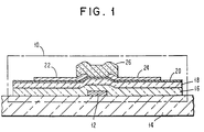
- an amorphous silicon thin film transistor 10 is shown.
- a metal gate electrode 12 is positioned on the surface of a glass substrate 14.
- Gate insulator layers 16 and 18 are positioned over the gate electrode 12 and substrate 14.
- a thin amorphous silicon layer 20 is on top of the gate insulator layers 16 and 18.
- Source electrode 22 and drain electrode 24 are formed on top of the thin amorphous layer 20.
- a second amorphous silicon layer 26 covers both the source 22 and drain 24 electrodes.
- the amorphous silicon layer 26 is necessary only when the first amorphous silicon layer cannot easily be made 30 nm or thicker. This amount of silicon is necessary to manufacture electrically useful devices.
- Prior art processes do not allow sufficient light through the structure at these thicknesses of silicon to expose the photoresist adequately. However, through the use of the present invention, short exposure times and high contrast photo images can be made and the amorphous silicon layer 26 can be eliminated.
- the substrate 14 need not be glass, but can also be a plastic transparent to the lithographically active wavelength provided that its thermal, mechanical and electrical properties are compatible with the processing and the intended use. It can theoretically be made of any transparent material such as sapphire, aluminas or more expensive glasses. However, when thin film transistors are used in large display panels the cost of the materials makes them less preferred. Similarly, more exotic and expensive semiconductors could be used in the place of amorphous silicon 20 to increase the device speed and which would also have the similar light absorption problems. However, amorphous silicon, amorphous silicon-germanium, or amorphous silicon-carbon films are preferred in fabricating low-cost, large panel displays. The amorphous films are easier to work with and LCDs do not require fast response times.
- Plasma deposited amorphous silicon commonly known as hydrogenated amorphous silicon is particularly preferred because its electrical properties are well matched to the LCD requirements.
- the gate insulator layers 16 and 18 can be made of any transparent insulating material but the layer 16 must have a refractive index different than the substrate 14. Any inorganic thin film insulator, or polymer materials such as polyimide may be used. However, in the manufacture of low cost, large panel displays, silicon dioxide, SiO2, or silicon nitride, Si3N4, films are preferred. It is understood that silicon dioxide and silicon nitride include plasma CVD versions of these materials which are known to incorporate various amounts of hydrogen.
- a process for forming a thin film transistor such as one shown in Fig. 1 is described with references to Figs. 2a-2e.
- a gate electrode 12 is formed on a glass substrate 14.
- the gate electrode 12 may be formed of Ni-Cr or other suitable alloys.
- gate insulator layers 16 and 18 are deposited over the substrate 14 and gate electrode.
- only one gate insulator layer 16 may be deposited.
- An amorphous semiconductor layer 20 is deposited via a plasma or plasma CVD process.
- a positive photoresist layer 30 is applied to the entire surface, and UV light is transmitted through the substrate, insulator films 16, 18 and amorphous semiconductor material 20.
- the thicknesses of the insulator films 16, 18 are chosen to maximize the amount of photolithographically active light to the photoresist 30.
- a conductive layer 40 typically a metal such as aluminum is deposited over the structure.
- the photoresist film 30 is removed by a solvent, the conductive layer 40 deposited on the photoresist film is removed. This leaves a gap over the gate electrode 12.
- the part of layer 40 not removed in this lift-off process form the source electrode 22 and the drain electrode 24. Their edges in the gap, as formed in this process, are aligned with the edges of the gate electrode within a precision of the wavelength of the light. Patterning of the interconnections to 22 and 24 do not require the precision necessary for the gap.
- a second amorphous silicon layer 26 is deposited on the top surface of the structure and patterned so that it is left in the gap above the gate electrode 12 and covers at least a portion of both source electrode 22 and drain electrode 24.
- a gate electrode 12, gate insulator layer 16, an amorphous silicon layer 20 and a capping layer 25 are consecutively deposited on a glass substrate 14.
- the gate insulator layer 16 or capping layer 25 can be composed of one or more transparent films. However, only one is illustrated.
- a photoresist film 30, which may be a positive type AZ1350J is applied and exposed to UV rays.
- the capping layer 25 must have a refractive index different than that of the photoresist 30.
- the gate electrode 12 is light impermeable and acts as a mask for the photoresist film 30.
- the film 30 is then used as a mask to selectively remove the exposed portion of capping layer 25. This can be done with an etchant which will etch insulator layers such as SiO2 and Si3N4 but which will not attack the amorphous semiconductor layer 20.
- Aluminum, or another metal, is deposited and then selectively removed by means of a lift-off or metal etch process, so as to form the source electrode 22 and the drain electrode 24 depicted in Fig. 3d.
- the capping layer 25 between the source and drain electrodes 22, 24 may be removed and additional amorphous silicon 26 deposited over the gate electrode.
- the exposure rate of the photoresist 30 used in preparing the lift-off stencil in both the processes shown in Figs. 2b and 3b is proportional to flux of the photolithographically active light ultimately absorbed by the resist. This flux can be increased by increasing (1) the light output of the light source, (2) the fraction of the light absorbed by the photoresist, or (3). the fraction of the light transmitted by the structure in-between the light source and the photoresist. More precisely, in the language of mathematics, the exposure rate is proportional to the integral over all lithographically active wavelengths of the product of the emission spectrum of the light source, of the absorption spectrum of the sensitizer of the resist, and of the transmission spectrum of the intervening structure.
- the light absorption in the Shipley AZ-1350 or equivalent positive resist starts at a wavelength of approximately 460 nm, but becomes strong only below 420 nm.
- Lithographic tools used for transmitting light through the structures typically employ mercury arc lamps as light sources. Therefore, the spectrum of the lamp consists of mercury lines, the 366 nm group being dominant. On the short wavelength side, the useful range is limited by the absorption in glass plates to about 320 nm. Although there is some contribution to resist exposure from the 405 and 436nm lines, the lithographically active light can be considered as nearly monochromatic at 366nm. Therefore to practice this invention with standard lithographic tools and resists, it is adequate to design the structure in a manner that its transmittance is maximized for the single wavelength of 366 nm.
- the transmittance of multilayer structures for monochromatic light is predicted by well-known theory described in Principles of Optics, by Max Born and Emil Wolf, published by Pergamon Press, sixth edition, 1980. Briefly, the transmittance of a multilayer structure is that fraction of the incident light which is not lost to absorption, reflection, or scattering. Scattering is a negligible loss mechanism in the structures considered here. Absorption is minimized if the light traverses the absorbing layer only once, that is by minimizing multiple reflections on either side of the absorbing layer that cause the light to travel back and forth. Reflection takes place whenever light traverses an interface at which the refractive index changes.
- the intensity of the reflected light from a multilayer structure is minimized if the wave components reflected at the various interfaces interfere destructively, which happens when their amplitudes are 180 degrees out of phase.
- the above cited reference gives a more thorough description of the phenomena involved, and provides formulae for the calculation of the absorbance, the reflectance, and hence the transmittance of such multilayer structures for any combination of layer thicknesses to enable one to calculate the optimal thicknesses.
- it is easier to use available digital computer programs which have been constructed to compute if the optical constants of the materials comprising the layers are known, the transmittance of the structure and optimal choices for layer thicknesses.
- the mathematical formulae required to calculate the optimal thicknesses are known and are not themselves considered part of the present invention.
- Structure 1 illustrates that an improvement in transmission from 13.7 to 19.7 percent is achieved by simply replacing the 300 nm oxide with a properly chosen thickness of a dielectric with a refractive index in between that of the substrate and of the amorphous silicon film.
- the ratio of the optical thickness (nd) to the wavelength of light to give a maximum in transmittance in this example is 1.245. Similar maxima in transmission were computed for nd/ ⁇ values of 0.745, 1.745, 2.245, etc. separated by deep minima. Note that the maxima occur at optical thicknesses close to but not identical to odd multiples of one fourth the wavelength, which would be the prediction of an approximate theory that disregards absorption in the amorphous silicon layer.
- Structures 2 and 3 illustrate that interposing properly chosen thicknesses of silicon dioxide will achieve the same transmission maximum as optimal thicknesses of silicon nitride alone. These structures are useful if for electrical reasons silicon dioxide is preferred over nitride to be the insulator adjacent to the amorphous semiconductor.
- Structure 4 illustrates that a slight further improvement in transmission is achieved by interposing below the nitride layer a properly chosen thickness of a dielectric with refractive index lower than the substrate.
- Structures 5-7 illustrate that further increases in transmission can be obtained interposing between the amorphous semiconductor and the photoresist a properly chosen antireflective capping layers.
- Table I demonstrate that it is possible to tailor the insulator to maintain desired electrical characteristics of the final transistor while improving the transmittance.
- the thickness of the original a-Si:H film must be sufficient for device operation, which is presently thought to be minimum 30nm.
- the transmission of the structure is 4.1 percent. This is too low for practical applications.
- the transmission can be raised to 5.6%, and with the addition of a proper interlayer between the a-Si:H and the photoresist, 7.0% transmission should be achievable. With this amount of light transmission to the photoresist, successful lithography is much more feasible.
- Table I illustrates optimal choices of non-absorbing layer thicknesses in various structures to maximize transmission of 366 nm light.
- the thickness of the a-Si:H layer was kept fixed at 12.0 nm.
- the gate insulator could comprise more than the stated two layers. This might be useful if its function were, in addition to optimizing light transmission, to control more than one electrical property, say both the capacitance and the insulator-semiconductor interfacial charge density. Or it would be possible to fabricate the structures described above using more expensive semiconductors to speed the thin film transistor. As explained above, exotic semiconductors would be unnecessary in fabricating large panel liquid crystal displays. While the embodiments described have been thin film transistors for large panel LCDs, they have broader application wherever a photoresist layer is exposed through a series of layers one of which is a light scattering or light absorbing layer.
Landscapes
- Thin Film Transistor (AREA)
- Liquid Crystal (AREA)
Claims (5)
- Procédé de fabrication d'un dispositif semiconducteur à couches minces (10) sur un substrat transparent (14), dans lequel le matériau photorésistant est exposé à l'aide de lumière lithographiquement active qui traverse les couches successives du dispositif semiconducteur dont au moins une à une propriété d'absorption de la lumière, comprenant:
le dépôt d'une électrode de porte (12) sur ledit substrat transparent (14),
le dépôt d'au moins une couche isolante transparente (16, 18) sur ledit substrat (14) et ladite électrode de porte (12) avec un indice de réfraction différent de celui dudit substrat et ayant une épaisseur dont la dimension est choisie pour que les composantes d'onde de ladite lumière lithographiquement active réfléchie aux interfaces de la structure achevée interfèrent de façon destructive afin de rendre minimale la réflectance et maximale la transmission de ladite lumière lithographiquement active,
le dépôt d'une mince couche semiconductrice perméable à la lumière (20) sur ladite couche isolante transparente (16, 18) qui a une propriété d'absorption de la lumière,
l'application d'un matériau photorésistant (30) sur ladite couche semiconductrice (20), et
l'exposition de ladite couche photorésistante (30) par la lumière photolithographiquement transmise dans ledit substrat, ladite au moins une couche isolante transparente (16, 18) et ladite couche semiconductrice (20). - Procédé de fabrication d'un dispositif semiconducteur à couches minces selon la revendication 1, qui comprend en outre:
le dépôt d'une autre couche isolante transparente (25) sur ladite couche semiconductrice (20) ayant un indice de réfraction différent de celui dudit matériau résistant (30) et ayant une épaisseur dont la dimension est choisie pour que les composantes d'onde de ladite lumière lithographiquement active réfléchie aux interfaces de la structure achevée interfèrent de façon destructive pour rendre minimale la réflectance et maximale la transmission de ladite lumière lithographiquement active. - Procédé de fabrication d'un dispositif semiconducteur à couches minces selon l'une ou l'autre des revendications précédentes, dans lequel lesdites couches isolantes transparentes sont choisies dans le groupe des SiO₂ et Si₃N₄.
- Procédé de fabrication d'un dispositif semiconducteur à couches minces selon l'une quelconque des revendications précédentes, dans lequel ladite couche semiconductrice est du silicium amorphe.
- Procédé de fabrication d'un dispositif semiconducteur à couches minces selon l'une quelconque des revendications précédentes, dans lequel le substrat est du verre.
Applications Claiming Priority (2)
| Application Number | Priority Date | Filing Date | Title |
|---|---|---|---|
| US140699 | 1988-01-04 | ||
| US07/140,699 US4888632A (en) | 1988-01-04 | 1988-01-04 | Easily manufacturable thin film transistor structures |
Publications (3)
| Publication Number | Publication Date |
|---|---|
| EP0322590A2 EP0322590A2 (fr) | 1989-07-05 |
| EP0322590A3 EP0322590A3 (fr) | 1991-01-16 |
| EP0322590B1 true EP0322590B1 (fr) | 1993-08-11 |
Family
ID=22492423
Family Applications (1)
| Application Number | Title | Priority Date | Filing Date |
|---|---|---|---|
| EP88120045A Expired - Lifetime EP0322590B1 (fr) | 1988-01-04 | 1988-12-01 | Dispositif semi-conducteur à couche mince |
Country Status (4)
| Country | Link |
|---|---|
| US (1) | US4888632A (fr) |
| EP (1) | EP0322590B1 (fr) |
| JP (1) | JPH0695527B2 (fr) |
| DE (1) | DE3883188T2 (fr) |
Families Citing this family (17)
| Publication number | Priority date | Publication date | Assignee | Title |
|---|---|---|---|---|
| EP0251563A3 (fr) * | 1986-06-17 | 1991-01-09 | Tokyo Electric Co. Ltd. | Dispositif de conversion photoélectrique |
| GB2220792B (en) * | 1988-07-13 | 1991-12-18 | Seikosha Kk | Silicon thin film transistor and method for producing the same |
| US5157470A (en) * | 1989-02-27 | 1992-10-20 | Hitachi, Ltd. | Thin film transistor, manufacturing method thereof and matrix circuit board and image display device each using the same |
| GB2235326A (en) * | 1989-08-16 | 1991-02-27 | Philips Electronic Associated | Active matrix liquid crystal colour display devices |
| US5322807A (en) * | 1992-08-19 | 1994-06-21 | At&T Bell Laboratories | Method of making thin film transistors including recrystallization and high pressure oxidation |
| JP3537854B2 (ja) * | 1992-12-29 | 2004-06-14 | エルジー フィリップス エルシーディー カンパニー リミテッド | 薄膜トランジスタの製造方法 |
| US6312968B1 (en) | 1993-06-30 | 2001-11-06 | The United States Of America As Represented By The Secretary Of The Navy | Method for fabricating an electrically addressable silicon-on-sapphire light valve |
| US6190933B1 (en) | 1993-06-30 | 2001-02-20 | The United States Of America As Represented By The Secretary Of The Navy | Ultra-high resolution liquid crystal display on silicon-on-sapphire |
| JP3478012B2 (ja) * | 1995-09-29 | 2003-12-10 | ソニー株式会社 | 薄膜半導体装置の製造方法 |
| US6127262A (en) * | 1996-06-28 | 2000-10-03 | Applied Materials, Inc. | Method and apparatus for depositing an etch stop layer |
| KR100333180B1 (ko) * | 1998-06-30 | 2003-06-19 | 주식회사 현대 디스플레이 테크놀로지 | Tft-lcd제조방법 |
| KR20010004604A (ko) * | 1999-06-29 | 2001-01-15 | 김영환 | 박막 트랜지스터 어레이 기판 및 그의 제조방법 |
| KR100709704B1 (ko) * | 2000-05-12 | 2007-04-19 | 삼성전자주식회사 | 액정 표시 장치용 박막 트랜지스터 기판 및 그 제조 방법 |
| US6746901B2 (en) * | 2000-05-12 | 2004-06-08 | Semiconductor Energy Laboratory Co., Ltd. | Semiconductor device and method of fabricating thereof |
| JP2004079901A (ja) * | 2002-08-21 | 2004-03-11 | Nec Electronics Corp | 半導体装置及びその製造方法 |
| KR100691319B1 (ko) * | 2004-09-15 | 2007-03-12 | 엘지.필립스 엘시디 주식회사 | 유기 박막 트랜지스터 및 그의 제조 방법 |
| US9401431B2 (en) * | 2009-04-21 | 2016-07-26 | Cbrite Inc. | Double self-aligned metal oxide TFT |
Family Cites Families (12)
| Publication number | Priority date | Publication date | Assignee | Title |
|---|---|---|---|---|
| US4040073A (en) * | 1975-08-29 | 1977-08-02 | Westinghouse Electric Corporation | Thin film transistor and display panel using the transistor |
| US4742384A (en) * | 1978-02-01 | 1988-05-03 | Rca Corporation | Structure for passivating a PN junction |
| JPS5680133A (en) * | 1979-12-06 | 1981-07-01 | Chiyou Lsi Gijutsu Kenkyu Kumiai | Formation of pattern |
| JPS5692573A (en) * | 1979-12-26 | 1981-07-27 | Citizen Watch Co Ltd | Display panel |
| US4393572A (en) * | 1980-05-29 | 1983-07-19 | Rca Corporation | Method of making low leakage N-channel SOS transistors utilizing positive photoresist masking techniques |
| JPS5731179A (en) * | 1980-07-31 | 1982-02-19 | Sharp Corp | Formation of thin-film transistor |
| JPS58170067A (ja) * | 1982-03-31 | 1983-10-06 | Fujitsu Ltd | 薄膜トランジスタの製造方法 |
| FR2566186B1 (fr) * | 1984-06-14 | 1986-08-29 | Thomson Csf | Procede de fabrication d'au moins un transistor a effet de champ en couche mince et transistor obtenu par ce procede |
| JPH073871B2 (ja) * | 1985-01-29 | 1995-01-18 | セイコー電子工業株式会社 | 薄膜トランジスタ |
| FR2590409B1 (fr) * | 1985-11-15 | 1987-12-11 | Commissariat Energie Atomique | Procede de fabrication d'un transistor en couches minces a grille auto-alignee par rapport au drain et a la source de celui-ci et transistor obtenu par le procede |
| JPS62291067A (ja) * | 1986-06-10 | 1987-12-17 | Nec Corp | 薄膜トランジスタの製造方法 |
| EP0270323B1 (fr) * | 1986-11-29 | 1999-11-03 | Sharp Kabushiki Kaisha | Méthode de fabrication d'un transistor en couche mince |
-
1988
- 1988-01-04 US US07/140,699 patent/US4888632A/en not_active Expired - Fee Related
- 1988-12-01 DE DE88120045T patent/DE3883188T2/de not_active Expired - Fee Related
- 1988-12-01 EP EP88120045A patent/EP0322590B1/fr not_active Expired - Lifetime
- 1988-12-06 JP JP63307076A patent/JPH0695527B2/ja not_active Expired - Lifetime
Also Published As
| Publication number | Publication date |
|---|---|
| US4888632A (en) | 1989-12-19 |
| JPH0695527B2 (ja) | 1994-11-24 |
| JPH02329A (ja) | 1990-01-05 |
| EP0322590A2 (fr) | 1989-07-05 |
| DE3883188D1 (de) | 1993-09-16 |
| DE3883188T2 (de) | 1994-03-17 |
| EP0322590A3 (fr) | 1991-01-16 |
Similar Documents
| Publication | Publication Date | Title |
|---|---|---|
| EP0322590B1 (fr) | Dispositif semi-conducteur à couche mince | |
| US6809785B2 (en) | Semipermeable liquid crystal display device and manufacturing method thereof | |
| US7907226B2 (en) | Method of fabricating an array substrate for liquid crystal display device | |
| KR930007529B1 (ko) | 액티브매트릭스기판의 제조방법 | |
| US6359320B1 (en) | Thin-film transistor with lightly-doped drain | |
| KR102049685B1 (ko) | 저온 폴리실리콘 어레이 기판의 제조방법 | |
| US9244320B2 (en) | Liquid crystal display and manufacturing method thereof | |
| KR102733664B1 (ko) | 액정 표시 장치 및 이의 제조 방법 | |
| WO2017136967A1 (fr) | Procédé de fabrication de substrat de réseau et substrat de réseau | |
| US5254488A (en) | Easily manufacturable thin film transistor structures | |
| WO2011045960A1 (fr) | Transistor en couches minces, procédé de fabrication de celui-ci et dispositif d'affichage équipé de celui-ci | |
| KR100487899B1 (ko) | 반투과형 액정표시장치 및 그 제조방법 | |
| EP0842530A1 (fr) | Procede d'elaboration d'un transistor a couches minces a grille auto-alignee | |
| US20080182179A1 (en) | Gray tone mask and method for manufacturing the same | |
| JP2978176B2 (ja) | アクティブマトリクス基板の製造方法及び表示装置の製造方法 | |
| JPH0488641A (ja) | 薄膜トランジスタの製造方法 | |
| JPH07142737A (ja) | 薄膜トランジスタの製造方法 | |
| KR100936889B1 (ko) | 액정 표시 장치의 어레이 기판 및 그 제조 방법 | |
| JP2625913B2 (ja) | 薄膜トランジスタ | |
| KR100811643B1 (ko) | 다중층 구조 절연막의 일괄식각 방법 | |
| JP2852919B2 (ja) | 液晶表示装置 | |
| KR20020031764A (ko) | 액정표시장치용 어레이패널 및 그의 제조방법 | |
| JPH0730119A (ja) | 液晶表示装置用薄膜トランジスタの製造方法 | |
| KR100521267B1 (ko) | 반사형 액정표시장치 및 그 제조방법 | |
| KR100219477B1 (ko) | 반사형 박막 트랜지스터-액정 표시 소자 및 그 제조방법 |
Legal Events
| Date | Code | Title | Description |
|---|---|---|---|
| PUAI | Public reference made under article 153(3) epc to a published international application that has entered the european phase |
Free format text: ORIGINAL CODE: 0009012 |
|
| AK | Designated contracting states |
Kind code of ref document: A2 Designated state(s): DE FR GB |
|
| 17P | Request for examination filed |
Effective date: 19891117 |
|
| PUAL | Search report despatched |
Free format text: ORIGINAL CODE: 0009013 |
|
| AK | Designated contracting states |
Kind code of ref document: A3 Designated state(s): DE FR GB |
|
| RHK1 | Main classification (correction) |
Ipc: H01L 29/784 |
|
| 17Q | First examination report despatched |
Effective date: 19920313 |
|
| GRAA | (expected) grant |
Free format text: ORIGINAL CODE: 0009210 |
|
| AK | Designated contracting states |
Kind code of ref document: B1 Designated state(s): DE FR GB |
|
| REF | Corresponds to: |
Ref document number: 3883188 Country of ref document: DE Date of ref document: 19930916 |
|
| ET | Fr: translation filed | ||
| PLBE | No opposition filed within time limit |
Free format text: ORIGINAL CODE: 0009261 |
|
| STAA | Information on the status of an ep patent application or granted ep patent |
Free format text: STATUS: NO OPPOSITION FILED WITHIN TIME LIMIT |
|
| 26N | No opposition filed | ||
| PGFP | Annual fee paid to national office [announced via postgrant information from national office to epo] |
Ref country code: FR Payment date: 19951128 Year of fee payment: 8 |
|
| PGFP | Annual fee paid to national office [announced via postgrant information from national office to epo] |
Ref country code: DE Payment date: 19951229 Year of fee payment: 8 |
|
| PGFP | Annual fee paid to national office [announced via postgrant information from national office to epo] |
Ref country code: GB Payment date: 19961126 Year of fee payment: 9 |
|
| PG25 | Lapsed in a contracting state [announced via postgrant information from national office to epo] |
Ref country code: FR Effective date: 19970829 |
|
| PG25 | Lapsed in a contracting state [announced via postgrant information from national office to epo] |
Ref country code: DE Effective date: 19970902 |
|
| REG | Reference to a national code |
Ref country code: FR Ref legal event code: ST |
|
| PG25 | Lapsed in a contracting state [announced via postgrant information from national office to epo] |
Ref country code: GB Free format text: LAPSE BECAUSE OF NON-PAYMENT OF DUE FEES Effective date: 19971201 |
|
| GBPC | Gb: european patent ceased through non-payment of renewal fee |
Effective date: 19971201 |