EP0322718B1 - Dispositif à effet tunnel résonnant - Google Patents
Dispositif à effet tunnel résonnant Download PDFInfo
- Publication number
- EP0322718B1 EP0322718B1 EP88121317A EP88121317A EP0322718B1 EP 0322718 B1 EP0322718 B1 EP 0322718B1 EP 88121317 A EP88121317 A EP 88121317A EP 88121317 A EP88121317 A EP 88121317A EP 0322718 B1 EP0322718 B1 EP 0322718B1
- Authority
- EP
- European Patent Office
- Prior art keywords
- resonant tunneling
- layer
- quantum well
- barrier layers
- tunneling device
- Prior art date
- Legal status (The legal status is an assumption and is not a legal conclusion. Google has not performed a legal analysis and makes no representation as to the accuracy of the status listed.)
- Expired - Lifetime
Links
- 230000005641 tunneling Effects 0.000 title claims description 49
- 230000004888 barrier function Effects 0.000 claims description 25
- 229910001218 Gallium arsenide Inorganic materials 0.000 claims description 18
- 239000004065 semiconductor Substances 0.000 claims description 14
- 229910000530 Gallium indium arsenide Inorganic materials 0.000 claims description 3
- 238000000034 method Methods 0.000 description 10
- 238000010586 diagram Methods 0.000 description 5
- 229910000980 Aluminium gallium arsenide Inorganic materials 0.000 description 4
- 230000000694 effects Effects 0.000 description 4
- 238000001451 molecular beam epitaxy Methods 0.000 description 3
- 238000004088 simulation Methods 0.000 description 3
- 239000000758 substrate Substances 0.000 description 3
- VYPSYNLAJGMNEJ-UHFFFAOYSA-N Silicium dioxide Chemical compound O=[Si]=O VYPSYNLAJGMNEJ-UHFFFAOYSA-N 0.000 description 2
- 238000003877 atomic layer epitaxy Methods 0.000 description 2
- 238000005229 chemical vapour deposition Methods 0.000 description 2
- 238000004519 manufacturing process Methods 0.000 description 2
- 238000001741 metal-organic molecular beam epitaxy Methods 0.000 description 2
- 229910052681 coesite Inorganic materials 0.000 description 1
- 229910052906 cristobalite Inorganic materials 0.000 description 1
- 239000007772 electrode material Substances 0.000 description 1
- 229910052737 gold Inorganic materials 0.000 description 1
- 238000002347 injection Methods 0.000 description 1
- 239000007924 injection Substances 0.000 description 1
- 238000003475 lamination Methods 0.000 description 1
- 238000005259 measurement Methods 0.000 description 1
- 239000002184 metal Substances 0.000 description 1
- 229910052751 metal Inorganic materials 0.000 description 1
- 229910052759 nickel Inorganic materials 0.000 description 1
- 238000000206 photolithography Methods 0.000 description 1
- 239000000377 silicon dioxide Substances 0.000 description 1
- 229910052682 stishovite Inorganic materials 0.000 description 1
- 239000010409 thin film Substances 0.000 description 1
- 229910052905 tridymite Inorganic materials 0.000 description 1
- 229910052721 tungsten Inorganic materials 0.000 description 1
Images


Classifications
-
- B—PERFORMING OPERATIONS; TRANSPORTING
- B82—NANOTECHNOLOGY
- B82Y—SPECIFIC USES OR APPLICATIONS OF NANOSTRUCTURES; MEASUREMENT OR ANALYSIS OF NANOSTRUCTURES; MANUFACTURE OR TREATMENT OF NANOSTRUCTURES
- B82Y10/00—Nanotechnology for information processing, storage or transmission, e.g. quantum computing or single electron logic
-
- H—ELECTRICITY
- H10—SEMICONDUCTOR DEVICES; ELECTRIC SOLID-STATE DEVICES NOT OTHERWISE PROVIDED FOR
- H10D—INORGANIC ELECTRIC SEMICONDUCTOR DEVICES
- H10D62/00—Semiconductor bodies, or regions thereof, of devices having potential barriers
- H10D62/80—Semiconductor bodies, or regions thereof, of devices having potential barriers characterised by the materials
- H10D62/81—Semiconductor bodies, or regions thereof, of devices having potential barriers characterised by the materials of structures exhibiting quantum-confinement effects, e.g. single quantum wells; of structures having periodic or quasi-periodic potential variation
- H10D62/815—Semiconductor bodies, or regions thereof, of devices having potential barriers characterised by the materials of structures exhibiting quantum-confinement effects, e.g. single quantum wells; of structures having periodic or quasi-periodic potential variation of structures having periodic or quasi-periodic potential variation, e.g. superlattices or multiple quantum wells [MQW]
- H10D62/8161—Semiconductor bodies, or regions thereof, of devices having potential barriers characterised by the materials of structures exhibiting quantum-confinement effects, e.g. single quantum wells; of structures having periodic or quasi-periodic potential variation of structures having periodic or quasi-periodic potential variation, e.g. superlattices or multiple quantum wells [MQW] potential variation due to variations in composition or crystallinity, e.g. heterojunction superlattices
- H10D62/8162—Semiconductor bodies, or regions thereof, of devices having potential barriers characterised by the materials of structures exhibiting quantum-confinement effects, e.g. single quantum wells; of structures having periodic or quasi-periodic potential variation of structures having periodic or quasi-periodic potential variation, e.g. superlattices or multiple quantum wells [MQW] potential variation due to variations in composition or crystallinity, e.g. heterojunction superlattices having quantum effects only in the vertical direction, i.e. layered structures having quantum effects solely resulting from vertical potential variation
- H10D62/8164—Semiconductor bodies, or regions thereof, of devices having potential barriers characterised by the materials of structures exhibiting quantum-confinement effects, e.g. single quantum wells; of structures having periodic or quasi-periodic potential variation of structures having periodic or quasi-periodic potential variation, e.g. superlattices or multiple quantum wells [MQW] potential variation due to variations in composition or crystallinity, e.g. heterojunction superlattices having quantum effects only in the vertical direction, i.e. layered structures having quantum effects solely resulting from vertical potential variation comprising only semiconductor materials
-
- H—ELECTRICITY
- H10—SEMICONDUCTOR DEVICES; ELECTRIC SOLID-STATE DEVICES NOT OTHERWISE PROVIDED FOR
- H10D—INORGANIC ELECTRIC SEMICONDUCTOR DEVICES
- H10D8/00—Diodes
- H10D8/70—Tunnel-effect diodes
- H10D8/755—Resonant tunneling diodes [RTD]
Definitions
- the present invention relates to a negative resistance element utilizing a resonant tunneling phenomenon in a semiconductor multi-barrier structure, and more particularly to a resonant tunneling device which can provide a negative resistance characteristic having substantially uniform or equal peak current values and can be used as a multiple (three or more) state logic element.
- the conventional tunneling device employs a double-layer structure in which a semiconductor layer (or thin film) having a narrow energy bandgap is sandwiched by two semiconductor layers each having a wide energy bandgap, as is disclosed by the article entitled “Room Temperature Observation of Differential Negative Resistance in an AlAs/GaAs/AlAs Resonant Tunneling Diode", Japanese Journal of Applied Physics, Vol. 24, pp. L466-L468, 1985 and the article entitled “Observation of Resonant Tunneling Via First Excited Level in Double-Barrier Diode", Electronics Letters, Vol. 22, No. 8, pp.
- Figs. 2A and 2B show the above-mentioned double-barrier and triple-barrier structures in energy band diagram for conduction band, respectively.
- quantum levels E 0 , E 1 , --- are formed in a quantum well layer 5 between first and second barrier layers 1 and 2 and a peak appears in a tunnel current each time the quantum level becomes equal to a quasi-Fermi level E F l on the cathode side through application of a voltage V.
- each of the conventional tunneling devices exhibits remarkably different peak current values, as shown in Fig. 3, and hence it is difficult to use it as a multiple state logic element.
- each of peak voltages V 1 , V 2 , --- is determined by quantum levels formed in one quantum well and hence it is difficult to control the peak voltages independently from each other.
- CAPASSO et al. "Resonant tunneling through double barriers, perpendicular quantum transport phenomena in superlattices, and their device applications"
- a superlattice structure including an interlaminated structure of three or more quantum well layers, wherein a resonant tunneling phenomenon is produced between discretely quantized energy levels formed in adjacent quantum wells.
- An object of the present invention is to provide a resonant tunneling device for a multi-state logical element which can provide a negative resistance characteristic having substantially equal peak current values and allowing independent control of peak voltages.
- three quantum levels are formed by providing an interlaminated structure of three semiconductor layers each having a narrow energy bandgap and serving as a quantum well layer and four semiconductor layers each having a wide energy bandgap and serving as a barrier layer, and a resonant tunneling phenomenon produced between the quantum levels is utilized to provide a resonant tunneling device which has substantially equal peak current values and high peak-to-valley (P.V) ratios.
- the three semiconductor layers having narrow energy bandgaps are termed first, second and third quantum well layers from the cathode electrode side, peak voltages V 1 and V 2 can be independently changed by the thicknesses of the third and second quantum well layers, respectively.
- the resonant tunneling device exhibits an excellent performance as a three state logic element for a logic circuit.
- Fig. 1 shows an energy band diagram for conduction band in a resonant tunneling device having a quadruple-barrier structure according to an embodiment of the present invention.
- the resonant tunneling device includes an interlaminated structure of three semiconductor layers each of which has a narrow energy bandgap and which serve as first, second and third quantum well layers 5, 6 and 7 and four semiconductor layers each of which has a wide energy bandgap and which serve as first, second, third and fourth barrier layers 1, 2, 3 and 4.
- Three quantum levels E 0 1 , E 0 2 and E 0 3 are formed and resonant tunnel effects of E 0 1 ⁇ E 0 3 and E 0 1 ⁇ E 0 2 are exhibited.
- Fig. 4 shows the current versus voltage characteristic obtained through simulation for a quadruple-barrier resonant tunneling device according to an embodiment of the present invention.
- the device includes a successive lamination of AlAs (10 ⁇ thickness), GaAs (119 ⁇ ), AlGaAs (30 ⁇ ), GaAs (57 ⁇ ), AlGaAs (30 ⁇ ), GaAs (69 ⁇ ) and AlAs (10 ⁇ ) and further includes n + type GaAs layers for cathode and anode each of which has a carrier concentration of 1x10 18 cm -3 . From Fig.
- a negative resistance characteristic is obtained with first and second peak currents having values substantially equal to each other, and three stable points are obtained by virtue of a load line shown in the figure.
- the first and second current peaks are caused by a resonant tunneling phenomenon as will be explained just below.
- Figs. 5A and 5B show the quantum levels for conduction band and the existence probabilities of electrons corresponding to first and second current peaks, respectively.
- the first current peak is caused by a resonant tunneling from a quantum level E 0 1 in a first quantum well layer 5 to a quantum level E 0 3 in a third quantum well layer 7, and the second current peak is caused by a resonant tunneling from the quantum level E 0 1 in the first quantum well layer 5 to a quantum level E 0 2 in a second quantum well layer 6. Therefore, peak voltages V 1 and V 2 (see Fig. 4) can be independently changed by the widths or thicknesses of the third and second quantum well layers 7 and 6, respectively.
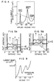
- FIG. 6A shows the peak voltages V 1 and V 2 in the case where the width Lw 2 of the second quantum well layer 6 is fixed to 57 ⁇ and the width Lw 3 of the third quantum well layer 7 is changed. It is seen from Fig. 6A that when Lw 3 is changed, the peak voltage V 2 has no change but the peak voltage V 1 greatly changes.
- Fig. 6B shows the case where Lw 3 is fixed to 69 ⁇ and Lw 2 is changed. It is seen from Fig. 6B that only the peak voltage V 2 has a substantial change.
- the resonant tunneling device has two clear or distinct current peaks in its current versus voltage characteristic, and the first and second peak voltages can be independently changed by the widths or thicknesses of the third and second quantum well layers, respectively.
- an n + type GaAs layer 9 having a carrier concentration of 1x10 18 cm -3 and a thickness of 2000 ⁇ and an i-type GaAs layer 10 having a thickness of 50 ⁇ are grown on an n + type GaAs substrate 8 through an MBE (Molecular Beam Epitaxy) method. Thereafter, a superlattice layer 11 and an n + type GaAs layer 12 having a carrier concentration of 1x10 18 cm -3 and a thickness of 3000 ⁇ are grown on the i-GaAs layer 10.
- the superlattice layer 11 includes a first barrier layer 27 made of i-AlAs and 10 ⁇ thick, a first quantum well layer 26 made of i-GaAs and 119 ⁇ thick, a second barrier layer 25 made of i-Al 0.3 Ga 0.7 As and 30 ⁇ thick, a second quantum well layer 24 made of i-GaAs and 57 ⁇ thick, a third barrier layer 23 made of i-Al 0.3 Ga 0.7 As and 30 ⁇ thick, a third quantum well layer 22 made of i-GaAs and 69 ⁇ thick, and a fourth barrier layer 21 made of i-AlAs and 10 ⁇ thick in this order from the n + type GaAs layer 12.
- the quantum well layers have in their widths a relation of the first quantum well layer 26 (on the cathode side) > the third quantum well layer 22 (on the anode side) > the second quantum well layer 24.
- the MBE method has been used as an epitaxial growth method.
- an MOCVD (Metal Organic Chemical Vapor Deposition) method, an MOMBE (Metal Organic Molecular Beam Epitaxy) method, an ALE (Atomic Layer Epitaxy) method or the like may be employed as the epitaxial growth method.
- a mesa region 13 is formed through a usual photolithography technique, as shown in Fig. 7B.
- an SiO 2 layer 14 having a thickness of 4000 ⁇ is grown by means of a CVD method, as shown in Fig. 7C.
- a cathode electrode 15 and an anode electrode 16 are formed by means of a usual lift-off method.
- AuGe, W, Ni and Au as electrode materials are vapor-deposited with 600 ⁇ , 100 ⁇ , 100 ⁇ and 800 ⁇ , respectively.
- the current versus voltage characteristic of the resonant tunneling device thus fabricated has been measured, and the result of measurement is shown in Fig. 8.
- a peak-to-valley (P/V) ratio is as high as it is about 3/1 for the first peak and about 1.5/1 for the second peak.
- a similar effect is also obtained when i-AlAs layers (10 ⁇ ) are used in place of the i-Al 0.3 Ga 0.7 As layers 23 and 25 (30 ⁇ ) in the superlattice layer 11.
- the similar effect is further obtained when an n + type InP substrate, InGaAs layers, InAlGaAs or InAlAs layers, and InAlAs layers are used in place of the n + type GaAs substrate 8, the GaAs layers 22, 24, 26, the AlGaAs layers 23, 25, and the AlAs layers 21, 27, respectively.
- a resonant tunneling device which has peak current values substantially equal to each other, peak voltages capable of being set independently from each other, and high peak-to-valley (P/V) ratios.
- P/V peak-to-valley
- the present invention has been explained in conjunction with the quadruple-barrier resonant tunneling device which can be used as a three state logic element.
- the present invention may be realized in conjunction with the quadruple-barrier resonant tunneling device which can be used as a three state logic element.
- a resonant tunneling device which can be used as a multiple (four or more) state logic element.
Landscapes
- Engineering & Computer Science (AREA)
- Chemical & Material Sciences (AREA)
- Nanotechnology (AREA)
- Physics & Mathematics (AREA)
- Mathematical Physics (AREA)
- Theoretical Computer Science (AREA)
- Crystallography & Structural Chemistry (AREA)
- Bipolar Transistors (AREA)
Claims (9)
- Dispositif à effet tunnel résonnant comportant une électrode (15) formant cathode, une électrode (16) formant anode et une couche de super-réseau (11) située entre celles-ci, dans lequel ladite couche de super-réseau a une structure interlaminée constituée d'au moins une première, deuxième, troisième et quatrième couche (1, 2, 3, 4; 27, 25, 23, 21) formant barrière, chacune étant constituée d'un semi-conducteur ayant une bande d'énergie interdite étroite, et d'au moins une première, deuxième et troisième couche (5, 6, 7; 26, 24, 22) formant puits quantique, chacune étant constituée d'un semi-conducteur ayant une bande d'énergie interdite large, dans cet ordre, à partir du côté où se trouve l'électrode formant cathode,
caractérisé en ce que
l'épaisseur de ladite première couche (5; 26) formant puits quantique est supérieure à celle de ladite troisième couche (7 ; 22) formant puits quantique qui est à son tour supérieure à celle de ladite deuxième couche (6; 24) formant puits quantique, le niveau d'énergie du premier état propre le plus bas, au niveau duquel se trouvent principalement les électrons dans ladite première couche formant puits quantique, est inférieur au niveau dégénéré occupé le plus haut dans ladite électrode (15) formant cathode, de sorte que lorsque des valeurs de tension définies sont appliquées auxdites électrodes (15, 16) formant cathode et anode, des phénomènes d'effet tunnel résonnant sont produits entre le niveau d'énergie du deuxième état propre le plus bas, au niveau duquel se trouvent principalement les électrons dans ladite troisième couche formant puits quantique, et ledit niveau d'énergie dudit premier état propre le plus bas, et entre le niveau d'énergie du troisième état propre le plus bas, au niveau duquel se trouvent principalement les électrons dans ladite deuxième couche formant puits quantique, et ledit niveau d'énergie dudit premier état propre le plus bas. - Dispositif à effet tunnel résonnant selon la revendication 1, dans lequel une caractéristique de résistance négative est produite par lesdits phénomènes d'effet tunnel résonnant de sorte que l'on a des valeurs de courant de crête pratiquement identiques les unes aux autres.
- Dispositif à effet tunnel résonnant selon la revendication 1 ou 2, dans lequel chacune desdites première, deuxième, troisième et quatrième couche (27, 25, 23, 21) formant barrière inclut une couche de AlxGa1-xAs, x étant un rapport de composition de Al sur Ga, et chacune desdites première, deuxième et troisième couche (26, 24, 22) formant puits quantique inclut une couche de GaAs.
- Dispositif à effet tunnel résonnant selon la revendication 3, dans lequel le rapport de composition x de Al sur Ga n'est pas inférieur à 0,8 pour lesdites première et quatrième couches (27, 21) formant barrière et tombe dans une plage comprise entre 0,2 et 0,4 pour lesdites deuxième et troisième couches (25, 23) formant barrière.
- Dispositif à effet tunnel résonnant selon la revendication 4, dans lequel le rapport de composition x de Al sur Ga est égal à 1,0 pour lesdites première et quatrième couches (27, 21) formant barrière et est égal à 0,3 pour lesdites deuxième et troisième couches (25, 23) formant barrière.
- Dispositif à effet tunnel résonnant selon l'une quelconque des revendications 1 à 5, dans lequel l'épaisseur de chacune desdites première et quatrième couches (27, 21) formant barrière tombe dans une plage comprise entre 8 Å et 50 Å et l'épaisseur de chacune desdites deuxième et troisième couches (25, 23) formant barrière tombe dans une plage comprise entre 10 Å et 100 Å.
- Dispositif à effet tunnel résonnant selon la revendication 6, dans lequel l'épaisseur de chacune desdites première et quatrième couches (27, 21) formant barrière est égale à 10 Å et l'épaisseur de chacune desdites deuxième et troisième couches (25, 23) formant barrière est égale à 30 Å.
- Dispositif à effet tunnel résonnant selon la revendication 1, dans lequel chacune desdites première, deuxième, troisième et quatrième couches formant barrière inclut une couche de InAlAs et chacune desdites première, deuxième et troisième couches formant puits quantique inclut une couche de InGaAs.
- Dispositif à effet tunnel résonnant selon la revendication 1, dans lequel chacune desdites première et quatrième couches formant barrière inclut une couche de InAlAs, chacune desdites deuxième et troisième couches formant barrière inclut une couche de InAlGaAs et chacune desdites première, deuxième et troisième couches formant puits quantique inclut une couche de InGaAS.
Applications Claiming Priority (2)
| Application Number | Priority Date | Filing Date | Title |
|---|---|---|---|
| JP62327155A JP2690922B2 (ja) | 1987-12-25 | 1987-12-25 | 共鳴トンネリング素子 |
| JP327155/87 | 1987-12-25 |
Publications (3)
| Publication Number | Publication Date |
|---|---|
| EP0322718A2 EP0322718A2 (fr) | 1989-07-05 |
| EP0322718A3 EP0322718A3 (fr) | 1990-03-21 |
| EP0322718B1 true EP0322718B1 (fr) | 1996-09-18 |
Family
ID=18195925
Family Applications (1)
| Application Number | Title | Priority Date | Filing Date |
|---|---|---|---|
| EP88121317A Expired - Lifetime EP0322718B1 (fr) | 1987-12-25 | 1988-12-20 | Dispositif à effet tunnel résonnant |
Country Status (4)
| Country | Link |
|---|---|
| US (1) | US5017973A (fr) |
| EP (1) | EP0322718B1 (fr) |
| JP (1) | JP2690922B2 (fr) |
| DE (1) | DE3855554D1 (fr) |
Families Citing this family (14)
| Publication number | Priority date | Publication date | Assignee | Title |
|---|---|---|---|---|
| EP0510557A3 (en) * | 1991-04-22 | 1994-06-22 | Nippon Telegraph & Telephone | Resonant tunneling transistor |
| GB2256746B (en) * | 1991-06-12 | 1995-05-03 | Marconi Gec Ltd | Semiconductor devices |
| USH1570H (en) * | 1993-03-31 | 1996-08-06 | The United States Of America As Represented By The Secretary Of The Army | Variable lateral quantum confinement transistor |
| JPH06318606A (ja) * | 1993-05-10 | 1994-11-15 | Mitsubishi Electric Corp | 半導体装置,並びにhbt素子及びhemt素子 |
| US5408107A (en) * | 1993-05-20 | 1995-04-18 | The Board Of Regents Of The University Of Texas System | Semiconductor device apparatus having multiple current-voltage curves and zero-bias memory |
| GB9421138D0 (en) * | 1994-10-20 | 1994-12-07 | Hitachi Europ Ltd | Memory device |
| US5535146A (en) * | 1995-04-27 | 1996-07-09 | National Science Council Of R.O.C. | Method for producing a semiconductor device using logic simulation approach to simulate a multi-peak resonant tunneling diode-based electronic circuit and a large signal multi-peak resonant tunneling diode spice model employed therefore |
| GB9724642D0 (en) | 1997-11-21 | 1998-01-21 | British Tech Group | Single electron devices |
| US6490193B1 (en) * | 2001-08-22 | 2002-12-03 | Raytheon Company | Forming and storing data in a memory cell |
| JP4747836B2 (ja) * | 2005-12-28 | 2011-08-17 | タカタ株式会社 | 乗員拘束装置 |
| JP5171539B2 (ja) * | 2007-11-29 | 2013-03-27 | キヤノン株式会社 | 共鳴トンネル構造体 |
| KR102113256B1 (ko) * | 2013-11-07 | 2020-05-20 | 삼성전자주식회사 | 다준위 에너지를 갖는 3중 연결 양자우물 구조를 포함하는 광학 소자 |
| US10170603B2 (en) * | 2016-08-08 | 2019-01-01 | Atomera Incorporated | Semiconductor device including a resonant tunneling diode structure with electron mean free path control layers |
| WO2022143028A1 (fr) * | 2020-12-30 | 2022-07-07 | 芯思杰技术(深圳)股份有限公司 | Structure de puits quantique, procédé de traitement de puces, puce et laser |
Family Cites Families (2)
| Publication number | Priority date | Publication date | Assignee | Title |
|---|---|---|---|---|
| DE3574082D1 (en) * | 1984-07-02 | 1989-12-07 | Texas Instruments Inc | Quantum-coupled device |
| JPS6158268A (ja) * | 1984-08-30 | 1986-03-25 | Fujitsu Ltd | 高速半導体装置 |
-
1987
- 1987-12-25 JP JP62327155A patent/JP2690922B2/ja not_active Expired - Lifetime
-
1988
- 1988-12-20 DE DE3855554T patent/DE3855554D1/de not_active Expired - Lifetime
- 1988-12-20 EP EP88121317A patent/EP0322718B1/fr not_active Expired - Lifetime
- 1988-12-21 US US07/287,738 patent/US5017973A/en not_active Expired - Fee Related
Non-Patent Citations (3)
| Title |
|---|
| IEEE ELECTRON DEVICE LETTERS vol.9, no.8, August 1988, New York, US; pages 365-367; T.TANOUE et al.:"A triple-well resonant-tunneling diode for multiple-valued logic application" * |
| IEEE TRANSACTIONS ON ELECTRON DEVICES vol.35, no.11, November 1988, New York, US; pages 1951-1956 H.MIZUTA et al.:"A new triple-well resonant tunneling diode with controllable double-negative resistance" * |
| stimulated resonant current in AlGaAs/GaAs triple barrier diodes" * |
Also Published As
| Publication number | Publication date |
|---|---|
| JPH01170055A (ja) | 1989-07-05 |
| EP0322718A2 (fr) | 1989-07-05 |
| US5017973A (en) | 1991-05-21 |
| JP2690922B2 (ja) | 1997-12-17 |
| DE3855554D1 (de) | 1996-10-24 |
| EP0322718A3 (fr) | 1990-03-21 |
Similar Documents
| Publication | Publication Date | Title |
|---|---|---|
| US4958201A (en) | Resonant tunneling minority carrier transistor | |
| US4575924A (en) | Process for fabricating quantum-well devices utilizing etch and refill techniques | |
| US5017973A (en) | Resonant tunneling device | |
| US4704622A (en) | Negative transconductance device | |
| US5148267A (en) | Double heterostructure step recovery diode with internal drift field | |
| US4959696A (en) | Three terminal tunneling device and method | |
| EP0256759B1 (fr) | Dispositif semi-conducteur à effet tunnel résonnant | |
| KR920006434B1 (ko) | 공진 터널링 장벽구조장치 | |
| US5059545A (en) | Three terminal tunneling device and method | |
| US4645707A (en) | Semiconductor devices | |
| US5886360A (en) | Semiconductor device | |
| US4851886A (en) | Binary superlattice tunneling device and method | |
| US5757025A (en) | Infrared photodetector using delta-doped semiconductors | |
| US5606178A (en) | Bipolar resonant tunneling transistor | |
| EP0186301B1 (fr) | Dispositif semi-conducteur à grande vitesse | |
| EP0363238B1 (fr) | Dispositif semi-conducteur à effet quantique ayant des propriétés de résistance différentielle négative | |
| EP0322773B1 (fr) | Dispositif à semi-conducteur avec élément semi-métal | |
| US6031245A (en) | Semiconductor device | |
| JPH0630399B2 (ja) | 共鳴トンネル・ダイオ−ド | |
| KR100222399B1 (ko) | 상온 고픽전류 공진 터널링 전자 장치 | |
| WO1987003424A1 (fr) | Dispositifs semiconducteurs | |
| Bonnefoi et al. | Uniformity in the electrical characteristics of GaAs/AlAs tunnel structures grown by metalorganic chemical vapor deposition | |
| KR100275499B1 (ko) | 에미터 서브-메사 어레이 구조를 갖는 양자 공진터널링 소자 | |
| Shimomura et al. | GaAsAl0. 3Ga0. 7As resonant tunneling diodes with atomically flat interfaces grown on (411) A GaAs substrates by MBE | |
| JP2710783B2 (ja) | 半導体装置 |
Legal Events
| Date | Code | Title | Description |
|---|---|---|---|
| PUAI | Public reference made under article 153(3) epc to a published international application that has entered the european phase |
Free format text: ORIGINAL CODE: 0009012 |
|
| AK | Designated contracting states |
Kind code of ref document: A2 Designated state(s): DE FR GB |
|
| PUAL | Search report despatched |
Free format text: ORIGINAL CODE: 0009013 |
|
| AK | Designated contracting states |
Kind code of ref document: A3 Designated state(s): DE FR GB |
|
| 17P | Request for examination filed |
Effective date: 19900921 |
|
| 17Q | First examination report despatched |
Effective date: 19921221 |
|
| GRAH | Despatch of communication of intention to grant a patent |
Free format text: ORIGINAL CODE: EPIDOS IGRA |
|
| GRAH | Despatch of communication of intention to grant a patent |
Free format text: ORIGINAL CODE: EPIDOS IGRA |
|
| GRAA | (expected) grant |
Free format text: ORIGINAL CODE: 0009210 |
|
| AK | Designated contracting states |
Kind code of ref document: B1 Designated state(s): DE FR GB |
|
| PG25 | Lapsed in a contracting state [announced via postgrant information from national office to epo] |
Ref country code: FR Effective date: 19960918 |
|
| REF | Corresponds to: |
Ref document number: 3855554 Country of ref document: DE Date of ref document: 19961024 |
|
| PG25 | Lapsed in a contracting state [announced via postgrant information from national office to epo] |
Ref country code: DE Effective date: 19961219 |
|
| EN | Fr: translation not filed | ||
| PLBE | No opposition filed within time limit |
Free format text: ORIGINAL CODE: 0009261 |
|
| STAA | Information on the status of an ep patent application or granted ep patent |
Free format text: STATUS: NO OPPOSITION FILED WITHIN TIME LIMIT |
|
| 26N | No opposition filed | ||
| PGFP | Annual fee paid to national office [announced via postgrant information from national office to epo] |
Ref country code: GB Payment date: 19970925 Year of fee payment: 10 |
|
| PG25 | Lapsed in a contracting state [announced via postgrant information from national office to epo] |
Ref country code: GB Free format text: LAPSE BECAUSE OF NON-PAYMENT OF DUE FEES Effective date: 19981220 |
|
| GBPC | Gb: european patent ceased through non-payment of renewal fee |
Effective date: 19981220 |