EP0324205B1 - Verstärkerschaltungsanordnung - Google Patents
Verstärkerschaltungsanordnung Download PDFInfo
- Publication number
- EP0324205B1 EP0324205B1 EP88202944A EP88202944A EP0324205B1 EP 0324205 B1 EP0324205 B1 EP 0324205B1 EP 88202944 A EP88202944 A EP 88202944A EP 88202944 A EP88202944 A EP 88202944A EP 0324205 B1 EP0324205 B1 EP 0324205B1
- Authority
- EP
- European Patent Office
- Prior art keywords
- resistor
- output
- transistors
- resistors
- reference point
- Prior art date
- Legal status (The legal status is an assumption and is not a legal conclusion. Google has not performed a legal analysis and makes no representation as to the accuracy of the status listed.)
- Expired - Lifetime
Links
- 230000008878 coupling Effects 0.000 claims description 2
- 238000010168 coupling process Methods 0.000 claims description 2
- 238000005859 coupling reaction Methods 0.000 claims description 2
- 238000004519 manufacturing process Methods 0.000 description 3
- 230000005669 field effect Effects 0.000 description 2
- 238000000034 method Methods 0.000 description 2
- 238000012986 modification Methods 0.000 description 2
- 230000004048 modification Effects 0.000 description 2
- 239000003990 capacitor Substances 0.000 description 1
- 238000010276 construction Methods 0.000 description 1
- 238000010586 diagram Methods 0.000 description 1
- 239000007787 solid Substances 0.000 description 1
Images
Classifications
-
- H—ELECTRICITY
- H03—ELECTRONIC CIRCUITRY
- H03F—AMPLIFIERS
- H03F1/00—Details of amplifiers with only discharge tubes, only semiconductor devices or only unspecified devices as amplifying elements
- H03F1/30—Modifications of amplifiers to reduce influence of variations of temperature or supply voltage or other physical parameters
- H03F1/302—Modifications of amplifiers to reduce influence of variations of temperature or supply voltage or other physical parameters in bipolar transistor amplifiers
Definitions
- This invention relates to an amplifier circuit arrangement having first and second stages in cascade, the first stage comprising a long tail pair of first and second transistors of the same conductivity type and first and second resistors coupling output electrodes of said first and second transistors respectively to a first voltage reference point and the second stage comprising a current amplifier circuit and a third resistor, the output electrode end of said first resistor being coupled to a second voltage reference point via said third resistor and the input current path of said current amplifier circuit in that order, and the output electrode end of said second resistor being coupled to said second voltage reference point via the output current path of said current amplifier circuit.
- an amplifier circuit arrangement as defined in the first paragraph is characterised in that a fourth resistor is included in series between the output electrode end of the second resistor and the output current path of the current amplifier circuit, in that the output current path end of said fourth resistor constitutes an output of the second stage, and in that the resistance values of said first, second, third and fourth resistors, and the gain of said current amplifier, are chosen such that in operation the voltage at the output of the second stage is substantially independent of variations in the potential on the first voltage reference point relative to the potential on the second voltage reference point.
- the output signal of the first stage can be coupled to the output of the second stage in such manner that any noise occurring at the first voltage reference point relative to the second voltage reference point will have little or no effect on the signal occurring at the output of the second stage, relative to the second voltage reference point.
- the signal at the output of the second stage (which stage may itself include transistors all of which are of said same conductivity type) can be applied in turn, for example, to the control electrode of a further transistor of said same conductivity type the common electrode of which is connected to the second voltage reference point (to which the "tail" of the long tail pair may conveniently be connected).
- control electrode output electrode
- common electrode common electrode
- base electrode collector electrode
- collector electrode collector electrode
- source electrode source electrode
- G of the current amplifier stage may, or course, be less than, equal to, or greater than unity.
- the second stage may include third and fourth transistors of said same conductivity type, the output electrodes of said third and fourth transistors being connected to said first voltage reference point, and the control electrode/common electrode paths of said third and fourth transistors being included between said output electrode end of said first resistor and said third resistor, and between said output electrode end of said second resistor and said fourth resistor, respectively.
- the third and fourth resistors may be connected directly to the first and second resistors respectively.
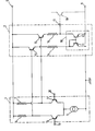
- an amplifier circuit arrangement comprises first and second stages 1 and 2 in cascade.
- the first stage 1 comprises a long tail pair of npn transistors 3 and 4 the collector electrodes of which are connected to a first voltage reference point 5 via first and second resistors 6 and 7 respectively.
- the commoned emitters of the transistors 3 and 4 are connected to a second voltage reference point 8 via a current source 9.
- the second stage 2 comprises a current amplifier circuit 10 which takes the form of a so-called current mirror circuit.
- Circuit 10 comprises a pair of npn transistors 11 and 12 the emitters of which are commoned and connected to the point 8. The bases of these transistors are also commoned and connected to the collector of transistor 11.
- the input current path of circuit 10 extends from the collector/base of transistor 11 to point 8, and the output current path thereof extends from the collector of transistor 12 to point 8.
- the collector end of resistor 6 is connected to the collector/bases of transistor 11 via the base-emitter path of an npn transistor 13 and a third resistor 14, in that order, and the collector end of resistor 7 is connected to the collector of transistor 12 via the base-emitter path of a transistor 15 and a fourth resistor 16, in that order.
- the collectors of transistors 13 and 15 are connected to point 8.
- the common point of resistor 16 and the collector of transistor 12 constitutes the output 17 of the stage 2, and may be connected to the base of a further npn transistor 18 if desired, as indicated in dashed lines.
- a positive supply potential is applied to point 5′ relative to point 8 and an input signal is applied between the bases of transistors 3 and 4 (points 19 and 20 respectively).
- the resulting differential signal voltages appearing at the collectors of the transistors 3 and 4 are applied to the input current path of amplifier 10 via emitter follower transistor 13 and resistor 14, and to the common point of the output current path of amplifier 10 and output terminal 17 via emitter follower transistor 15 and resistor 16, respectively.
- the resulting signal current flowing in the input path of amplifier 10 results in known manner in G times this signal current flowing in the output path of amplifier 10. The overall result is therefore that the output signal of stage 1 is successfully coupled to the output 17 of stage 2.
- the emitter follower transistors 13 and 15, which in effect constitute signal voltage sources of internal resistances R6/(1+B13) and R7/(1+B15) respectively connected between the ends of the resistors 14 and 16 and the point 5, are provided basically to reduce the load imposed on the output of stage 1 by the input of stage 2.
- respective capacitors may be provided across each of the resistors 14 and 16 to improve the frequency response of the arrangement. If such are provided the ratio between their impedances should be chosen equal to the ratio between the corresponding resistors 14 and 16.
- npn transistors in the circuits described may be replaced by pnp transistors if the sign of the supply voltage applied between points 5 and 8 is reversed. Alternatively they may be replaced by n-channel (or p-channel if the sign of the supply voltage is reversed) field effect transistors, the gates, drains and sources of the latter corresponding to the bases, collectors and emitters respectively of the bipolar transistors described.
- the simple current mirror construction shown for the amplifier 10 may of course be replaced by another form of current amplifier circuit, for example one of the many other current mirror circuits which are well-known to persons skilled in the art.
Landscapes
- Engineering & Computer Science (AREA)
- Power Engineering (AREA)
- Amplifiers (AREA)
Claims (5)
- Eine Verstärkerschaltungsanordnung mit einer ersten und zweiten Stufe in Kaskade, die erste Stufe verfügt über ein langes Schwanzpaar erster und zweiter Transistoren desselben Konduktivitätstyps und erste und zweite Widerstände, die die Ausgangselektroden der besagten ersten und zweiten Transistoren jeweils mit einem ersten Spannungsreferenzpunkt verbinden, und die zweite Stufe verfügt über eine Stromverstärkerschaltung und einen dritten Widerstand, wobei das Ende der Ausgangselektrode des besagten ersten Widerstands über den besagten dritten Widerstand und in dieser Reihenfolge über die Stromeingangsleitung der besagten Stromverstärkerschaltung mit einem zweiten Spannungsreferenzpunkt und das Ende der Ausgangselektrode des besagten zweiten Widerstands über die Stromausgangsleitung der besagten Stromverstärkerschaltung mit einen zweiten Spannungsreferenzpunkt verbunden ist, mit dem Merkmal, daß ein vierter Widerstand in Serie zwischen dem Ende der Ausgangselektrode des zweiten Widerstands und der Stromausgangsleitung der Stromverstärkerschaltung enthalten ist, daß das Ende der Stromausgangsleitung des besagten vierten Widerstands einen Ausgang der zweiten Stufe bildet und, daß die Widerstandswerte des ersten, zweiten, dritten und vierten Widerstands und die Leistung des besagten Stromverstärkers so gewählt werden, daß bei Betrieb die Spannung am Ausgang der zweiten Stufe grundlegend unabhängig von Spannungsvariationen des ersten Spannungsreferenzpunktes in bezug auf die Spannung des zweiten Spannungsreferenzpunktes ist.
- Eine Anordnung laut Anspruch 1, bei der die zweite Stufe über Transistoren verfügt, die alle desselben Konduktivitätstyps sind.
- Eine Anordnung laut Anspruch 1 oder Anspruch 2, wobei die zweite Stufe einen dritten und vierten Transistor des besagten gleichen Konduktivitätstyps aufweisen kann und die Ausgangselektroden der besagten dritten und vierten Transistoren an den ersten Spannungsreferenzpunkt angeschlossen werden und die Leitungen der Prüfelektrode/gemeinsamen Elektrode des besagten dritten und vierten Transistors zwischen dem Ende der Ausgangselektrode des besagten ersten Widerstands und des besagten dritten und jeweils zwischen dem Ende der besagten Ausgangselektrode des besagten zweiten Widerstands und des besagten dritten Widerstands eingefügt sind.
- Eine Anordnung laut Anspruch 1 oder Anspruch 2, wobei die Widerstandswerte des besagten dritten und vierten Widerstands in bezug auf die Widerstandswerte des besagten jeweiligen ersten und zweiten Widerstands hoch sind und der dritte und vierte Widerstand direkt an jeweils den ersten und zweiten Widerstand angeschlossen wird.
- Eine Anordnung laut einem der vorgenannten Ansprüche, wobei der Schwanz des langen Schwanzpaars an den zweiten Spannungsreferenzpunkt angeschlossen ist.
Applications Claiming Priority (2)
| Application Number | Priority Date | Filing Date | Title |
|---|---|---|---|
| GB8730137A GB2214375A (en) | 1987-12-24 | 1987-12-24 | Amplifier circuit arrangement |
| GB8730137 | 1987-12-24 |
Publications (3)
| Publication Number | Publication Date |
|---|---|
| EP0324205A2 EP0324205A2 (de) | 1989-07-19 |
| EP0324205A3 EP0324205A3 (en) | 1990-09-19 |
| EP0324205B1 true EP0324205B1 (de) | 1996-03-27 |
Family
ID=10629049
Family Applications (1)
| Application Number | Title | Priority Date | Filing Date |
|---|---|---|---|
| EP88202944A Expired - Lifetime EP0324205B1 (de) | 1987-12-24 | 1988-12-19 | Verstärkerschaltungsanordnung |
Country Status (5)
| Country | Link |
|---|---|
| US (1) | US4920321A (de) |
| EP (1) | EP0324205B1 (de) |
| JP (1) | JP2774120B2 (de) |
| DE (1) | DE3855157T2 (de) |
| GB (1) | GB2214375A (de) |
Families Citing this family (5)
| Publication number | Priority date | Publication date | Assignee | Title |
|---|---|---|---|---|
| US5510745A (en) * | 1987-07-29 | 1996-04-23 | Fujitsu Limited | High-speed electronic circuit having a cascode configuration |
| US5304869A (en) * | 1992-04-17 | 1994-04-19 | Intel Corporation | BiCMOS digital amplifier |
| JPH07111484A (ja) * | 1993-08-20 | 1995-04-25 | Hitachi Ltd | 無線通信装置 |
| US5917349A (en) * | 1997-10-09 | 1999-06-29 | Kabushiki Kaisha Toshiba | Current mode driver using N-type transistors |
| JP2002057532A (ja) * | 2000-08-11 | 2002-02-22 | Nec Corp | 線形トランスコンダクタンスアンプ |
Family Cites Families (7)
| Publication number | Priority date | Publication date | Assignee | Title |
|---|---|---|---|---|
| US3444476A (en) * | 1965-03-19 | 1969-05-13 | Rca Corp | Direct coupled amplifier with feedback for d.c. error correction |
| FR1529717A (fr) * | 1967-04-19 | 1968-06-21 | Sfim | Amplificateur différentiel à courant continu et à liaison directe |
| JPS6090407A (ja) * | 1983-10-24 | 1985-05-21 | Toshiba Corp | 差動増幅器 |
| JPS62274923A (ja) * | 1986-05-23 | 1987-11-28 | Hitachi Ltd | 半導体装置 |
| US4710728A (en) * | 1986-06-30 | 1987-12-01 | Motorola, Inc. | Amplifier having improved gain-bandwidth product |
| US4767946A (en) * | 1987-01-12 | 1988-08-30 | Tektronix, Inc. | High-speed supply independent level shifter |
| JPS63240109A (ja) * | 1987-03-27 | 1988-10-05 | Toshiba Corp | 差動増幅器 |
-
1987
- 1987-12-24 GB GB8730137A patent/GB2214375A/en not_active Withdrawn
-
1988
- 1988-12-19 DE DE3855157T patent/DE3855157T2/de not_active Expired - Fee Related
- 1988-12-19 EP EP88202944A patent/EP0324205B1/de not_active Expired - Lifetime
- 1988-12-22 US US07/289,650 patent/US4920321A/en not_active Expired - Lifetime
- 1988-12-23 JP JP63323772A patent/JP2774120B2/ja not_active Expired - Lifetime
Non-Patent Citations (1)
| Title |
|---|
| Journal of Solid State Electronics, vol.SC-22, no.2, April 1987. * |
Also Published As
| Publication number | Publication date |
|---|---|
| DE3855157T2 (de) | 1996-10-02 |
| GB2214375A (en) | 1989-08-31 |
| JP2774120B2 (ja) | 1998-07-09 |
| EP0324205A2 (de) | 1989-07-19 |
| EP0324205A3 (en) | 1990-09-19 |
| GB8730137D0 (en) | 1988-02-03 |
| US4920321A (en) | 1990-04-24 |
| JPH01202907A (ja) | 1989-08-15 |
| DE3855157D1 (de) | 1996-05-02 |
Similar Documents
| Publication | Publication Date | Title |
|---|---|---|
| EP0058448B1 (de) | Steilheitsverstärker | |
| JPS63107210A (ja) | 差電圧−電流変換器 | |
| EP0600852B1 (de) | Logik-Schaltungsanordnungen | |
| US4661779A (en) | Operational amplifier | |
| US4573020A (en) | Fully differential operational amplifier with D.C. common-mode feedback | |
| US5028881A (en) | Highly linear operational transconductance amplifier with low transconductance | |
| US4797629A (en) | Wide range operational amplifier input stage | |
| US5469092A (en) | Electronic circuit including means for reflecting signal current and feed forward means for compensating operational speed thereof | |
| US3534279A (en) | High current transistor amplifier stage operable with low current biasing | |
| US4978868A (en) | Simplified transistor base current compensation circuitry | |
| US5332937A (en) | Transconductor stage for high frequency filters | |
| US5485074A (en) | High ratio current mirror with enhanced power supply rejection ratio | |
| US4884039A (en) | Differential amplifier with low noise offset compensation | |
| US4912427A (en) | Power supply noise rejection technique for amplifiers | |
| EP0324205B1 (de) | Verstärkerschaltungsanordnung | |
| JPH0550163B2 (de) | ||
| US4890067A (en) | Common base configuration for an fT doubler amplifier | |
| US4779057A (en) | Cascode amplifier with nonlinearity correction and improve transient response | |
| EP0164182A1 (de) | JFET Eingangsstufe mit aktiver Last | |
| US4550291A (en) | Noise-free, die area efficient cascode circuit | |
| US4730124A (en) | High transconductance composite PNP transistor | |
| US4928073A (en) | DC amplifier | |
| US5136258A (en) | Circuit arrangement for enhancing the transconductance of a differential amplifier stage comprising MOS transistors | |
| US5334949A (en) | Differential amplifiers | |
| CN116895320A (zh) | 用于复制电流的器件 |
Legal Events
| Date | Code | Title | Description |
|---|---|---|---|
| PUAI | Public reference made under article 153(3) epc to a published international application that has entered the european phase |
Free format text: ORIGINAL CODE: 0009012 |
|
| AK | Designated contracting states |
Kind code of ref document: A2 Designated state(s): DE FR GB IT NL |
|
| PUAL | Search report despatched |
Free format text: ORIGINAL CODE: 0009013 |
|
| AK | Designated contracting states |
Kind code of ref document: A3 Designated state(s): DE FR GB IT NL |
|
| 17P | Request for examination filed |
Effective date: 19910315 |
|
| RAP3 | Party data changed (applicant data changed or rights of an application transferred) |
Owner name: N.V. PHILIPS' GLOEILAMPENFABRIEKEN Owner name: PHILIPS ELECTRONICS UK LIMITED |
|
| 17Q | First examination report despatched |
Effective date: 19930210 |
|
| GRAA | (expected) grant |
Free format text: ORIGINAL CODE: 0009210 |
|
| AK | Designated contracting states |
Kind code of ref document: B1 Designated state(s): DE FR GB IT NL |
|
| PG25 | Lapsed in a contracting state [announced via postgrant information from national office to epo] |
Ref country code: NL Free format text: LAPSE BECAUSE OF FAILURE TO SUBMIT A TRANSLATION OF THE DESCRIPTION OR TO PAY THE FEE WITHIN THE PRESCRIBED TIME-LIMIT Effective date: 19960327 |
|
| REF | Corresponds to: |
Ref document number: 3855157 Country of ref document: DE Date of ref document: 19960502 |
|
| ITF | It: translation for a ep patent filed | ||
| ET | Fr: translation filed | ||
| NLV1 | Nl: lapsed or annulled due to failure to fulfill the requirements of art. 29p and 29m of the patents act | ||
| PLBE | No opposition filed within time limit |
Free format text: ORIGINAL CODE: 0009261 |
|
| STAA | Information on the status of an ep patent application or granted ep patent |
Free format text: STATUS: NO OPPOSITION FILED WITHIN TIME LIMIT |
|
| 26N | No opposition filed | ||
| REG | Reference to a national code |
Ref country code: FR Ref legal event code: CD |
|
| PGFP | Annual fee paid to national office [announced via postgrant information from national office to epo] |
Ref country code: DE Payment date: 20010214 Year of fee payment: 13 |
|
| PGFP | Annual fee paid to national office [announced via postgrant information from national office to epo] |
Ref country code: FR Payment date: 20011221 Year of fee payment: 14 |
|
| PGFP | Annual fee paid to national office [announced via postgrant information from national office to epo] |
Ref country code: GB Payment date: 20011224 Year of fee payment: 14 |
|
| REG | Reference to a national code |
Ref country code: GB Ref legal event code: IF02 |
|
| PG25 | Lapsed in a contracting state [announced via postgrant information from national office to epo] |
Ref country code: DE Free format text: LAPSE BECAUSE OF NON-PAYMENT OF DUE FEES Effective date: 20020702 |
|
| PG25 | Lapsed in a contracting state [announced via postgrant information from national office to epo] |
Ref country code: GB Free format text: LAPSE BECAUSE OF NON-PAYMENT OF DUE FEES Effective date: 20021219 |
|
| GBPC | Gb: european patent ceased through non-payment of renewal fee |
Effective date: 20021219 |
|
| PG25 | Lapsed in a contracting state [announced via postgrant information from national office to epo] |
Ref country code: FR Free format text: LAPSE BECAUSE OF NON-PAYMENT OF DUE FEES Effective date: 20030901 |
|
| REG | Reference to a national code |
Ref country code: FR Ref legal event code: ST |
|
| PG25 | Lapsed in a contracting state [announced via postgrant information from national office to epo] |
Ref country code: IT Free format text: LAPSE BECAUSE OF NON-PAYMENT OF DUE FEES;WARNING: LAPSES OF ITALIAN PATENTS WITH EFFECTIVE DATE BEFORE 2007 MAY HAVE OCCURRED AT ANY TIME BEFORE 2007. THE CORRECT EFFECTIVE DATE MAY BE DIFFERENT FROM THE ONE RECORDED. Effective date: 20051219 |