EP0324308A2 - Méthode et système de décodage d'instructions de plusieurs formats incompatibles - Google Patents
Méthode et système de décodage d'instructions de plusieurs formats incompatibles Download PDFInfo
- Publication number
- EP0324308A2 EP0324308A2 EP88480070A EP88480070A EP0324308A2 EP 0324308 A2 EP0324308 A2 EP 0324308A2 EP 88480070 A EP88480070 A EP 88480070A EP 88480070 A EP88480070 A EP 88480070A EP 0324308 A2 EP0324308 A2 EP 0324308A2
- Authority
- EP
- European Patent Office
- Prior art keywords
- instruction
- instructions
- store
- address
- fetched
- Prior art date
- Legal status (The legal status is an assumption and is not a legal conclusion. Google has not performed a legal analysis and makes no representation as to the accuracy of the status listed.)
- Granted
Links
Images



Classifications
-
- G—PHYSICS
- G06—COMPUTING OR CALCULATING; COUNTING
- G06F—ELECTRIC DIGITAL DATA PROCESSING
- G06F9/00—Arrangements for program control, e.g. control units
- G06F9/06—Arrangements for program control, e.g. control units using stored programs, i.e. using an internal store of processing equipment to receive or retain programs
- G06F9/30—Arrangements for executing machine instructions, e.g. instruction decode
- G06F9/38—Concurrent instruction execution, e.g. pipeline or look ahead
- G06F9/3818—Decoding for concurrent execution
- G06F9/3822—Parallel decoding, e.g. parallel decode units
-
- G—PHYSICS
- G06—COMPUTING OR CALCULATING; COUNTING
- G06F—ELECTRIC DIGITAL DATA PROCESSING
- G06F9/00—Arrangements for program control, e.g. control units
- G06F9/06—Arrangements for program control, e.g. control units using stored programs, i.e. using an internal store of processing equipment to receive or retain programs
- G06F9/30—Arrangements for executing machine instructions, e.g. instruction decode
-
- G—PHYSICS
- G06—COMPUTING OR CALCULATING; COUNTING
- G06F—ELECTRIC DIGITAL DATA PROCESSING
- G06F9/00—Arrangements for program control, e.g. control units
- G06F9/06—Arrangements for program control, e.g. control units using stored programs, i.e. using an internal store of processing equipment to receive or retain programs
- G06F9/30—Arrangements for executing machine instructions, e.g. instruction decode
- G06F9/30145—Instruction analysis, e.g. decoding, instruction word fields
-
- G—PHYSICS
- G06—COMPUTING OR CALCULATING; COUNTING
- G06F—ELECTRIC DIGITAL DATA PROCESSING
- G06F9/00—Arrangements for program control, e.g. control units
- G06F9/06—Arrangements for program control, e.g. control units using stored programs, i.e. using an internal store of processing equipment to receive or retain programs
- G06F9/30—Arrangements for executing machine instructions, e.g. instruction decode
- G06F9/30145—Instruction analysis, e.g. decoding, instruction word fields
- G06F9/3016—Decoding the operand specifier, e.g. specifier format
- G06F9/30167—Decoding the operand specifier, e.g. specifier format of immediate specifier, e.g. constants
-
- G—PHYSICS
- G06—COMPUTING OR CALCULATING; COUNTING
- G06F—ELECTRIC DIGITAL DATA PROCESSING
- G06F9/00—Arrangements for program control, e.g. control units
- G06F9/06—Arrangements for program control, e.g. control units using stored programs, i.e. using an internal store of processing equipment to receive or retain programs
- G06F9/30—Arrangements for executing machine instructions, e.g. instruction decode
- G06F9/3017—Runtime instruction translation, e.g. macros
- G06F9/30174—Runtime instruction translation, e.g. macros for non-native instruction set, e.g. Javabyte, legacy code
-
- G—PHYSICS
- G06—COMPUTING OR CALCULATING; COUNTING
- G06F—ELECTRIC DIGITAL DATA PROCESSING
- G06F9/00—Arrangements for program control, e.g. control units
- G06F9/06—Arrangements for program control, e.g. control units using stored programs, i.e. using an internal store of processing equipment to receive or retain programs
- G06F9/30—Arrangements for executing machine instructions, e.g. instruction decode
- G06F9/30181—Instruction operation extension or modification
- G06F9/30185—Instruction operation extension or modification according to one or more bits in the instruction, e.g. prefix, sub-opcode
-
- G—PHYSICS
- G06—COMPUTING OR CALCULATING; COUNTING
- G06F—ELECTRIC DIGITAL DATA PROCESSING
- G06F9/00—Arrangements for program control, e.g. control units
- G06F9/06—Arrangements for program control, e.g. control units using stored programs, i.e. using an internal store of processing equipment to receive or retain programs
- G06F9/30—Arrangements for executing machine instructions, e.g. instruction decode
- G06F9/30181—Instruction operation extension or modification
- G06F9/30196—Instruction operation extension or modification using decoder, e.g. decoder per instruction set, adaptable or programmable decoders
Definitions
- This invention relates to computer processor architecture and operational methods in general, and in particular to a method of decoding plural incompatible format instructions.
- One general architectural approach to resolving the compatibility problem involves reservation of a bit or some bit combination in the instruction format for the machine that is to run the program.
- the extra bit or bit combinations are utilized to flag instructions which are non-native format for the machine. Whenever such a flag combination is encountered, the instruction containing it can be decoded using different rules from the native instruction decode rules.
- This scheme allows non-native instructions to be located anywhere in the instruction store, but does so at the expense and inconvenience of lengthening the native instruction word by adding the additional bit or bit combinations. This has the effect of using up available instruction decode permutations that might otherwise be used for more beneficial purposes within the machine.
- Another architectural approach which is related to the previously discussed one, is to establish an instruction type mode switching control, which may be operated by executing a particular instruction.
- the purpose of the "switch" instruction is to permit the programmer to switch the host machine's instruction decoding mode from one type to another when moving among instructions of various types or formats. This requires that the "switch" instruction be included in all subroutine or subprogram entry and exit points which adds unnecessarily to the complication of writing programs and increases the amount of program storage required.
- variable decode logic to contain the specifications for decoding the machine instructions.
- a programmer may tailor an instruction set to suit the application or task which is to be programmed.
- This approach also provides a means for allowing machine language programs written in one format for one type of machine to be run in another type of machine which is not normally compatible with the first machine's instruction format.
- the technique does not permit mixing of machine language instruction types or formats in a single machine.
- instructions from different machine types that are written in different formats that are normally incompatible may be placed or intermixed in the instruction storage of a single machine and still may be decoded and executed properly.
- the instructions, as loaded, are segregated or mapped into areas of the instruction store which are uniquely associated with containing instructions of a given format or type. Either specific regions of the instruction store may be reserved for each type or format of instruction, or instruction types identified to the link editor may be loaded and a table or map maintained of the locations in storage and the format type of instruction that is contained therein.
- the instructions may be then fetched sequentially in normal mode for decoding and execution in the machine.
- a three-phase pipelined data processor architecture is illustrated in the descriptions which follow.
- an instruction is first fetched on one cycle, decoded in the second cycle and executed in the third cycle by the processor's arithmetic logic unit.
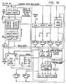
- Instructions reside in the instruction store 2 in Figure 1 and are fetched into the instruction decoding register 1 for decoding by the instruction decoding logic.
- the decoding logic which may consist of some form of memory or may be implemented in a more conventional way using standard logic elements (i.e., ANDS, ORs, etc.), is used to transform fetched instructions to a form appropriate to operate the gates and controls of the processor flow logic in such a way that the desired instruction execute actions take place.
- the transformed instruction is then placed in the Execute Register 4, at the end of decode phase.
- the instruction address register 3 provides the next instruction address to instruction store 2 over the instruction address bus IAB. Instructions are sequentially fetched and placed in the instruction decode register 1 and portions of the instruction are examined in the address resolving logic 6 which contains logic that defines which field or fields of the instruction are to be used and (perhaps) modified to produce an effective address or direct operand value.
- address resolving logic 6 contains logic that defines which field or fields of the instruction are to be used and (perhaps) modified to produce an effective address or direct operand value.
- decode tables in the instruction decoding memory or logic 5 may be loaded externally on line 9. This may provide the loading of specific instruction decoding rules as will be later described.
- the instruction decode register 1 abbreviated IDR
- the IDR is the register into which instructions fetched from the instruction store, called I-store 2, are placed to be decoded. Instructions taken from, or “fetched” from, the I-store 2 are placed in the IDR where they are held for decoding. The instructions are stored in the IDR prior to being decoded in the instruction decoding logic or memory 5.
- the instruction address register 3, abbreviated IAR in Figure 1 is used to contain the I-store 2 address for the instruction that is to be fetched.
- the execution register 4, abbreviated EXR contains decoded instructions which are the execution process codes for the specific machine.
- Instruction decoding logic elements comprising the instruction decode memory or logic as explained earlier, with its contained logic, and the address resolving logic 6 are utilized for decoding the instructions that reside in the IDR 1.
- the address resolving logic extracts specific bits from the instruction in the IDR, based upon the instruction type, and then causes an effective address or immediate operand value to be calculated by adding (for example) the contents of some index register (R0 or R4 in Figure 1B).
- I-store 2 is assumed to be separate from a data store (not shown) and is thus a "harvard" architectural design for the machine. Loading instructions into I-store 2 may be accomplished previously by loading or writing a ROM or RAM chip with the instructions outside of the host machine. Alternatively, I-store is RAM, and may be written using special instructions in the host processor repertoire for this purpose. When this is done, the path is via IDB with IAR providing the write address.
- the pipelined processor operates in such fashion that instructions fetched from the I-store 2 are placed in the IDR 1 at the end of a fetch cycle. This corresponds to the start of a decoding cycle. Then, during the decoding cycle, the instruction contained in the IDR 1 is recoded to a new form appropriate for execution by the processor. Simultaneously, the address resolving logic 6 extracts the appropriate instruction bits and calculates an effective address or immediate value. The end of the decoding cycle, which results in the loading of the decoded bits into EXR 4 and resolved address or immediate value data into the CABR, represents the start of the execution cycle.
- the pipelined processor phases thus overlap: while one instruction is being fetched, the instruction previously fetched into the IDR is being decoded and an instruction previously decoded into the EXR 4 is being executed.
- the instruction decode logic in Figure 1 is shown as contained in instruction decode memory IDM 5. In the arrangement shown, some or all of the bits from the instruction being decoded in the IDR 1 are used as a portion of the address utilized to look up a decoded instruction code. Which specific bits or fields of the IDR are used in the resolved address is determined by the address resolving logic 6 as will be described later in greater detail.
- the content of the instruction decode memory IDM 5 at any particular address is, in fact, the execution code for a particular decoded instruction. As shown in Figure 1, a path 9 for loading the contents of the IDM 5 with decode information codes may be included, although this is not generally present in most machines.
- the general concept of placing instruction decoding tables in memory is extended in the present invention to permit placing instructions in various normally incompatible machine languages or formats into the instruction store, and yet allow for proper decoding.
- the overall object is to permit the programmer to mix or comingle in memory the existing machine language formats or programs that may have originally been written for two or more different machine types and to permit execution of all of the code on a single processor without modifying or recompiling the programs.
- a single program which may consist of process instructions or entire sub-routines or code modules from dissimilar machines and in dissimilar or incompatible formats, must be link-edited.
- the well known function of the link editor program is to assign separately identified or otherwise segregated or mapped locations in the I-store 2 to the various portions of machine language code being used. This may be easily accomplished by reserving major segments, for example the high order address locations, for one language or format instruction type and the remaining segments in I-store for other languages or formats. An example of this follows later.
- the technique used in the present invention is represented as an extension of the basic concept of utilizing an instruction decode memory for containing instruction decode specifications or execution codes. This has been done for convenience in explaining the architecture and method of operation, but is not an essential portion of the idea since other forms of instruction decode logic are well known.
- the purpose of having a loadable instruction decode memory 5, as shown in this illustration, is to permit tailoring of the instruction set to any specific programming application. The implication is that each new program application will require its own unique decoding or execution code table. If, as is done in the present example, the machine is designed to accommodate and to decode and execute machine level instructions for two or more different or incompatible processors, the instruction decode memory contents will not generally need to be changed for each application. It is only when an additional new instruction set needs to be dealt with that the IDM 5 would have to be loaded with new tables.
- Figure 2 illustrates a block diagram of the major portions of the logic required to accommodate the changes proposed by the preferred embodiment of this invention.
- the logic shown is similar to that in Figure 1, but omits the ILR 8 and its loading line 7 for simplicity and includes only the elements necessary for implementing the multiple instruction type decoding of the present invention.
- Figure 2 shows an example of the instruction store 2 with partitioning illustrated for accommodating two types of different, incompatible format machine language instructions.
- the high order addresses have been arbitrarily reserved for machine type or format 2 instructions. These are identified as having the high order address beginning with 111 in binary and reserve 1/8 of the instruction store total capacity for machine type 2 instructions. The remaining addresses are arbitrarily reserved for machine type 1 instructions as illustrated.
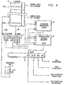
- FIG. 2 illustrates the addition of a new component, the Instruction Decode Selection Register, IDSR, 10.
- IDSR Instruction Decode Selection Register
- This element is a register that is operated so that it retains the instruction address or some portion thereof of the instruction currently residing in IDR 1.
- the IDSR 10 is used to trap or retain the address of the last instruction that was fetched from I-store 2.
- the IDSR 10 retains a portion of the address of the last instruction fetched and will be clocked with the same signal that causes the IDR 1 to be loaded. The retained portion may be all of the address or less if required. Thus, it will always receive the address of the instruction that is loaded into the IDR 1.
- IDSR 10 is assumed to contain only the high order three bits from the IAR 3 because of the arbitrarily assumed partitioning of I-store 2 in the instant example. Only the three high order bits necessary to define which of the eight equal arbitrary segments of I-store or partitions are being addressed.
- IDSR 10 and of IDR 1 are taken together in Figure 2 to provide a look-up address within the IDM 5. Only specific portions of the undecoded instruction in IDR may be needed according to the format of the instruction being fetched.
- the other portion of the input address to the IDM 5 is the output from the IDSR 10 which identifies the fetched-from address in I-store 2, or in the instant example, at least the range in which the address lies within I-store 2. Decoding of any specific instruction in the IDR 1 thus depends not only on the contents of the IDR 1 but on the region of the I-store 2 from which the instruction was fetched. This portion of the address is provided by the IDSR 10 output.
- IDSR 10 also has an output path to the address resolution logic 6. This is necessary to enable the logic to access the appropriate bit fields from the IDR 1 when an operand or effective address must be formed. In general, there will be no compatibility that can be expected between instruction sets of various machines with regard to the placement within the instruction, and the length of, any operand fields.
- the effect of using the fetched-from address, or portion of the address, which defines at least a field within the I-store regions, as a part of the access specifications for decoding the specific instruction that is fetched, is to permit instructions in different regions of I-store 2 to be decoded utilizing different rules.
- I-store 2 if a portion of I-store 2 is set aside for "type 2programs, as is shown in Figure 2, and if the instruction decode memory 5 is set up in the manner described above, all instructions fetched from the region of I-store 2 that are identified by the three high order address bits 111, will be decoded according to type 2 decode rules contained in IDM 5, and instructions fetched from the type 1 region in the I-store 2 will be decoded in the unique manner required for type 1 instructions.
- type 2 decode rules contained in IDM 5 if a portion of I-store 2 is set aside for "type 2programs, as is shown in Figure 2, and if the instruction decode memory 5 is set up in the manner described above, all instructions fetched from the region of I-store 2 that are identified by the three high order address bits 111, will be decoded according to type 2 decode rules contained in IDM 5, and instructions fetched from the type 1 region in the I-store 2 will be decoded in the unique manner required for type 1 instructions.
- the instruction store will be hypothetically partitioned as shown in Figure 2, and type 1 instructions would be located somewhere within the lower 7/8 of the addressing space in the I-store 2; type 2 instructions would be located in the upper 1/8 of the address spaces in I-store 2. This is accommodated prior to loading of the instructions into the I-store 2 from an external source through the ILR 8 as shown in Figure 1 when the instructions have been link edited and examined and have been assigned I-store addresses for loading in accordance with the type of instruction that they represent.
- the contents of the IDR 1 and the IDSR 10 are taken together to be used as the source of an address for looking up the decode execution code represented by the instruction in the IDM 5.
- the execution register 4 EXR will be loaded with the decoded instruction codes that were found in the IDM 5 at the location specified by the content of the IDR 1 and the IDSR 10 and IDR 1 and IDSR 10 will be loaded with the next instruction to be decoded and the address in I-store from which it was fetched, respectively.
- the state of the registers at the start of the execution cycle is indicated in Figure 6.
- the contents of the IDSR 10 and the IDR 1 are shown as Xs since, for the execution cycle, the contents of these registers is immaterial.
- the contents of the execution register EXR 4 shows an exemplary decode operation for an add registers operation in which the lower-most EXR register cell contains 2, an identification to the ALU of register 2 which is to be the source of its operand B.
- the next adjacent cell contains 3 which identifies to the ALU the source of its A operand, in this case register 3.
- the next field describes the function to be performed by the ALU, in this case 01, meaning an add register and the next field describes the carryin selection, in this case, 0 for an add register's function.
- IDR 1 when a type 2 "add registers" instruction is to be executed, then that instruction will be fetched in the normal sequential manner and placed into the IDR 1 just as the type 1 instructions were fetched before.
- the IAR 3 controls which address within the I-store 2 is next accessed and when type 2 instructions are reached, they will be decoded and executed in sequence as prescribed by whatever program has been written.
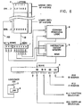
- IDSR 10 will receive the three high order address bits and will thus contain, in the example shown, the binary content 111 as illustrated in Figure 5.
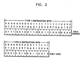
- IDR 1 will contain the hexidecimal code as illustrated in Figure 3 for the add register instruction in the type 2 format which is XX1A32.
- the register contents for IDSR 10 and IDR 1 are illustrated in Figure 5. It may be noted that since the type 2 add registers instruction has a word size of only 16 bits in the example assumed, it has been placed in the low order 16-bit positions in the IDR 1 and the high order bits are thus immaterial and are shown as Xs.
- IDR 1 and IDSR 10 contents, or portions thereof, are used together as the address for looking up the decode of the specific instruction of the type 2 add registers in the IDM 5 logic or memory.
- the two high order bytes of the IDR 1 will have no part in decoding of the instruction since they do not exist in type 2 instructions.
- the address used for IDM 5 will be entirely different from that used for looking up the decode of the type 1 instruction example just given.
- the instruction decode memory IDM 5 will be configured to contain the same pattern of decoded bits. That is, the execution code to be placed in EXR will be identical since exactly the same function is specified by both the type 1 add register's instruction and the type 2 add register's instruction. Therefore, the state of the execution register 4 after the type 2 add register's instruction has been successfully decoded is represented in Figure 6 as being just the same as it was for the type 1 instruction.
- the decode memory table or hardwired logic as used in the present invention will require somewhat greater content to support decodes of multiple instruction types or formats than those that are required to support a single instruction format or type. Also, certain conditions must be met or must pre-exist when multiple types of machine level instructions are to co-exist within a single machine for decoding and execution. The essential conditions are that the machine level instructions for one machine type to be executed directly in another require the executing machine to have at least equivalent data flow path widths and arithmetic logic resources.
- the data flow of the hosting machine must have a multiplier, and the relationship of the multiplier to other necessary arithmetic elements must be similar to those provided in the machine for which the original program was written.
- all instructions that reside in the I-store 2 of the machine must be able to fit within the word size of that I store.
- instructions from a 24-bit wide instruction word machine to be executed in a non-native host machine will require that the host machine have at least a 24-bit instruction word size of its own to accommodate those from the first machine.
- the address resolving facilities i.e., the number of index registers, the index adder sizes, etc., for the hosting machine must be adequate to accommodate the effective address and operand formation for the non-native machine instructions as will be evident to those of skill in the field.
Landscapes
- Engineering & Computer Science (AREA)
- Software Systems (AREA)
- Theoretical Computer Science (AREA)
- Physics & Mathematics (AREA)
- General Engineering & Computer Science (AREA)
- General Physics & Mathematics (AREA)
- Executing Machine-Instructions (AREA)
- Advance Control (AREA)
Applications Claiming Priority (2)
| Application Number | Priority Date | Filing Date | Title |
|---|---|---|---|
| US142585 | 1988-01-11 | ||
| US07/142,585 US5115500A (en) | 1988-01-11 | 1988-01-11 | Plural incompatible instruction format decode method and apparatus |
Publications (3)
| Publication Number | Publication Date |
|---|---|
| EP0324308A2 true EP0324308A2 (fr) | 1989-07-19 |
| EP0324308A3 EP0324308A3 (fr) | 1991-03-27 |
| EP0324308B1 EP0324308B1 (fr) | 1996-03-27 |
Family
ID=22500446
Family Applications (1)
| Application Number | Title | Priority Date | Filing Date |
|---|---|---|---|
| EP88480070A Expired - Lifetime EP0324308B1 (fr) | 1988-01-11 | 1988-11-08 | Méthode et système de décodage d'instructions de plusieurs formats incompatibles |
Country Status (4)
| Country | Link |
|---|---|
| US (1) | US5115500A (fr) |
| EP (1) | EP0324308B1 (fr) |
| JP (1) | JPH01201729A (fr) |
| DE (1) | DE3855158T2 (fr) |
Cited By (20)
| Publication number | Priority date | Publication date | Assignee | Title |
|---|---|---|---|---|
| GB2290395A (en) * | 1994-06-10 | 1995-12-20 | Advanced Risc Mach Ltd | Interoperability with multiple instruction sets |
| US5740461A (en) * | 1994-05-03 | 1998-04-14 | Advanced Risc Machines Limited | Data processing with multiple instruction sets |
| US5794010A (en) * | 1996-06-10 | 1998-08-11 | Lsi Logic Corporation | Method and apparatus for allowing execution of both compressed instructions and decompressed instructions in a microprocessor |
| US5867681A (en) * | 1996-05-23 | 1999-02-02 | Lsi Logic Corporation | Microprocessor having register dependent immediate decompression |
| US5896519A (en) * | 1996-06-10 | 1999-04-20 | Lsi Logic Corporation | Apparatus for detecting instructions from a variable-length compressed instruction set having extended and non-extended instructions |
| EP0820006A3 (fr) * | 1996-07-19 | 1999-04-28 | Philips Patentverwaltung GmbH | Processeur de signaux |
| RU2137184C1 (ru) * | 1994-05-03 | 1999-09-10 | Арм Лимитед | Отображение с помощью мультинаборов команд |
| WO2000008554A1 (fr) * | 1998-08-07 | 2000-02-17 | Koninklijke Philips Electronics N.V. | Appareil comportant une memoire de programme et un processeur |
| WO2000045257A3 (fr) * | 1999-01-28 | 2001-03-08 | Ati Int Srl | Execution de programmes destines a une premiere architecture d'ordinateur sur un ordinateur a seconde architecture |
| EP1124180A2 (fr) | 2000-02-08 | 2001-08-16 | Kabushiki Kaisha Toshiba | Système de traitement de données avec conversion de code d'instruction et procédé pour la génération d'instructions |
| EP0875893A3 (fr) * | 1997-03-27 | 2001-10-17 | Deutsche Thomson-Brandt Gmbh | Dispositif de traitement d'une séquence de commandes de contrôle, méthode de génération d'une séquence de commandes de contrôle, et support de stockage pour stocker une séquence de commandes de contrôle |
| EP1089167A3 (fr) * | 1999-10-01 | 2001-10-24 | Hitachi, Ltd. | Architecture de processeur pour l'exécution de deux jeux d'instructions différents à longueur fixe |
| GB2374694A (en) * | 2001-02-26 | 2002-10-23 | Advanced Risc Mach Ltd | Storing instruction set information |
| EP0808485A4 (fr) * | 1995-02-10 | 2003-01-02 | Intel Corp | Procede et appareil pour assurer la transition entre des jeux d'instructions dans un processeur |
| WO2004034253A3 (fr) * | 2002-10-11 | 2004-10-28 | Koninkl Philips Electronics Nv | Parallelisation d'instructions dependant de la plage d'adresse d'un appareil de traitement de donnees |
| US7020768B2 (en) | 2001-02-01 | 2006-03-28 | Arm Limited | Apparatus and method for facilitating debugging of sequences of processing instructions using context identifier comparison |
| US7107439B2 (en) | 2001-08-10 | 2006-09-12 | Mips Technologies, Inc. | System and method of controlling software decompression through exceptions |
| US7149878B1 (en) | 2000-10-30 | 2006-12-12 | Mips Technologies, Inc. | Changing instruction set architecture mode by comparison of current instruction execution address with boundary address register values |
| GB2435116B (en) * | 2006-02-10 | 2010-04-07 | Imagination Tech Ltd | Selecting between instruction sets in a microprocessors |
| US7707389B2 (en) | 2003-10-31 | 2010-04-27 | Mips Technologies, Inc. | Multi-ISA instruction fetch unit for a processor, and applications thereof |
Families Citing this family (50)
| Publication number | Priority date | Publication date | Assignee | Title |
|---|---|---|---|---|
| JP2835103B2 (ja) * | 1989-11-01 | 1998-12-14 | 富士通株式会社 | 命令指定方法及び命令実行方式 |
| US5349481A (en) * | 1993-06-10 | 1994-09-20 | Exabyte Corporation | Apparatus and method for distorted track data recovery by rewinding and re-reading the tape at a slower than nominal speed |
| US6496922B1 (en) * | 1994-10-31 | 2002-12-17 | Sun Microsystems, Inc. | Method and apparatus for multiplatform stateless instruction set architecture (ISA) using ISA tags on-the-fly instruction translation |
| US5619685A (en) * | 1994-11-04 | 1997-04-08 | Ball Corporation | Run-time dynamically adaptive computer process for facilitating communication between computer programs |
| JPH08339298A (ja) * | 1995-02-02 | 1996-12-24 | Ricoh Co Ltd | マイクロプロセッサにおける命令追加方法及びそれを用いたマイクロプロセッサ |
| KR100584964B1 (ko) * | 1996-01-24 | 2006-05-29 | 선 마이크로시스템즈 인코퍼레이티드 | 스택 메모리 구조에서의 캐싱 장치 |
| EP0976029A2 (fr) * | 1996-01-24 | 2000-02-02 | Sun Microsystems, Inc. | Processeur d'execution de jeux d'instructions re us d'un reseau ou d'une memoire locale |
| US6711667B1 (en) * | 1996-06-28 | 2004-03-23 | Legerity, Inc. | Microprocessor configured to translate instructions from one instruction set to another, and to store the translated instructions |
| US6049863A (en) * | 1996-07-24 | 2000-04-11 | Advanced Micro Devices, Inc. | Predecoding technique for indicating locations of opcode bytes in variable byte-length instructions within a superscalar microprocessor |
| US5867680A (en) * | 1996-07-24 | 1999-02-02 | Advanced Micro Devices, Inc. | Microprocessor configured to simultaneously dispatch microcode and directly-decoded instructions |
| US5925124A (en) * | 1997-02-27 | 1999-07-20 | International Business Machines Corporation | Dynamic conversion between different instruction codes by recombination of instruction elements |
| US5930491A (en) * | 1997-06-18 | 1999-07-27 | International Business Machines Corporation | Identification of related instructions resulting from external to internal translation by use of common ID field for each group |
| US6014513A (en) * | 1997-12-23 | 2000-01-11 | University Of Washington | Discovering code and data in a binary executable program |
| US6367047B1 (en) | 1998-10-20 | 2002-04-02 | Ecrix | Multi-level error detection and correction technique for data storage recording device |
| US6381706B1 (en) | 1998-10-20 | 2002-04-30 | Ecrix Corporation | Fine granularity rewrite method and apparatus for data storage device |
| US6246551B1 (en) | 1998-10-20 | 2001-06-12 | Ecrix Corporation | Overscan helical scan head for non-tracking tape subsystems reading at up to 1X speed and methods for simulation of same |
| US6307701B1 (en) | 1998-10-20 | 2001-10-23 | Ecrix Corporation | Variable speed recording method and apparatus for a magnetic tape drive |
| US6308298B1 (en) | 1998-11-16 | 2001-10-23 | Ecrix Corporation | Method of reacquiring clock synchronization on a non-tracking helical scan tape device |
| US6367048B1 (en) | 1998-11-16 | 2002-04-02 | Mcauliffe Richard | Method and apparatus for logically rejecting previously recorded track residue from magnetic media |
| US6603618B1 (en) | 1998-11-16 | 2003-08-05 | Exabyte Corporation | Method and system for monitoring and adjusting tape position using control data packets |
| US6421805B1 (en) | 1998-11-16 | 2002-07-16 | Exabyte Corporation | Rogue packet detection and correction method for data storage device |
| US8074055B1 (en) * | 1999-01-28 | 2011-12-06 | Ati Technologies Ulc | Altering data storage conventions of a processor when execution flows from first architecture code to second architecture code |
| US7065633B1 (en) | 1999-01-28 | 2006-06-20 | Ati International Srl | System for delivering exception raised in first architecture to operating system coded in second architecture in dual architecture CPU |
| US8121828B2 (en) * | 1999-01-28 | 2012-02-21 | Ati Technologies Ulc | Detecting conditions for transfer of execution from one computer instruction stream to another and executing transfer on satisfaction of the conditions |
| US6978462B1 (en) | 1999-01-28 | 2005-12-20 | Ati International Srl | Profiling execution of a sequence of events occuring during a profiled execution interval that matches time-independent selection criteria of events to be profiled |
| US6954923B1 (en) | 1999-01-28 | 2005-10-11 | Ati International Srl | Recording classification of instructions executed by a computer |
| US6763452B1 (en) | 1999-01-28 | 2004-07-13 | Ati International Srl | Modifying program execution based on profiling |
| US7013456B1 (en) | 1999-01-28 | 2006-03-14 | Ati International Srl | Profiling execution of computer programs |
| US8127121B2 (en) | 1999-01-28 | 2012-02-28 | Ati Technologies Ulc | Apparatus for executing programs for a first computer architechture on a computer of a second architechture |
| US7275246B1 (en) | 1999-01-28 | 2007-09-25 | Ati International Srl | Executing programs for a first computer architecture on a computer of a second architecture |
| US7111290B1 (en) * | 1999-01-28 | 2006-09-19 | Ati International Srl | Profiling program execution to identify frequently-executed portions and to assist binary translation |
| US7941647B2 (en) | 1999-01-28 | 2011-05-10 | Ati Technologies Ulc | Computer for executing two instruction sets and adds a macroinstruction end marker for performing iterations after loop termination |
| US6779107B1 (en) | 1999-05-28 | 2004-08-17 | Ati International Srl | Computer execution by opportunistic adaptation |
| US7254806B1 (en) | 1999-08-30 | 2007-08-07 | Ati International Srl | Detecting reordered side-effects |
| US6438664B1 (en) | 1999-10-27 | 2002-08-20 | Advanced Micro Devices, Inc. | Microcode patch device and method for patching microcode using match registers and patch routines |
| US6934832B1 (en) | 2000-01-18 | 2005-08-23 | Ati International Srl | Exception mechanism for a computer |
| US6624960B1 (en) | 2000-03-10 | 2003-09-23 | Exabyte Corporation | Current sensing drum/cleaning wheel positioning method and apparatus for magnetic storage system |
| US6364234B1 (en) | 2000-03-10 | 2002-04-02 | Michael Donald Langiano | Tape loop/slack prevention method and apparatus for tape drive |
| US20020004897A1 (en) * | 2000-07-05 | 2002-01-10 | Min-Cheng Kao | Data processing apparatus for executing multiple instruction sets |
| US6633969B1 (en) | 2000-08-11 | 2003-10-14 | Lsi Logic Corporation | Instruction translation system and method achieving single-cycle translation of variable-length MIPS16 instructions |
| US7711926B2 (en) * | 2001-04-18 | 2010-05-04 | Mips Technologies, Inc. | Mapping system and method for instruction set processing |
| US6826681B2 (en) | 2001-06-18 | 2004-11-30 | Mips Technologies, Inc. | Instruction specified register value saving in allocated caller stack or not yet allocated callee stack |
| US7698539B1 (en) * | 2003-07-16 | 2010-04-13 | Banning John P | System and method of instruction modification |
| US7606997B1 (en) * | 2003-07-18 | 2009-10-20 | Guillermo Rozas | Method and system for using one or more address bits and an instruction to increase an instruction set |
| US8006074B1 (en) * | 2003-12-24 | 2011-08-23 | Altera Corporation | Methods and apparatus for executing extended custom instructions |
| US20060155974A1 (en) * | 2005-01-07 | 2006-07-13 | Moyer William C | Data processing system having flexible instruction capability and selection mechanism |
| US7421568B2 (en) * | 2005-03-04 | 2008-09-02 | Qualcomm Incorporated | Power saving methods and apparatus to selectively enable cache bits based on known processor state |
| US7836285B2 (en) * | 2007-08-08 | 2010-11-16 | Analog Devices, Inc. | Implementation of variable length instruction encoding using alias addressing |
| EP2203814A4 (fr) * | 2007-09-19 | 2012-11-07 | Kpit Cummins Infosystems Ltd | Mécanisme pour activer des composants matériels plug and play pour une migration de logiciels semi-automatique |
| CN117369831B (zh) * | 2023-10-17 | 2024-12-17 | 西南民族大学 | 一种针对嵌入式处理器的反汇编方法 |
Family Cites Families (10)
| Publication number | Priority date | Publication date | Assignee | Title |
|---|---|---|---|---|
| US4455602A (en) * | 1981-05-22 | 1984-06-19 | Data General Corporation | Digital data processing system having an I/O means using unique address providing and access priority control techniques |
| US4499604A (en) * | 1981-05-22 | 1985-02-12 | Data General Corporation | Digital data processing system for executing instructions containing operation codes belonging to a plurality of operation code sets and names corresponding to name table entries |
| US4514800A (en) * | 1981-05-22 | 1985-04-30 | Data General Corporation | Digital computer system including apparatus for resolving names representing data items and capable of executing instructions belonging to general instruction sets |
| US4517642A (en) * | 1981-05-22 | 1985-05-14 | Data General Corporation | Digital computer system having unique means of referring to operands and ability to execute a plurality of internal languages |
| US4499535A (en) * | 1981-05-22 | 1985-02-12 | Data General Corporation | Digital computer system having descriptors for variable length addressing for a plurality of instruction dialects |
| US4575797A (en) * | 1981-05-22 | 1986-03-11 | Data General Corporation | Digital data processing system incorporating object-based addressing and capable of executing instructions belonging to several instruction sets |
| US4782461A (en) * | 1984-06-21 | 1988-11-01 | Step Engineering | Logical grouping of facilities within a computer development system |
| JPS6133546A (ja) * | 1984-07-25 | 1986-02-17 | Nec Corp | 情報処理装置 |
| US4800523A (en) * | 1985-02-25 | 1989-01-24 | Itt Corporation | Device interface controller having device specific and device common instructions separately stored |
| US4791557A (en) * | 1985-07-31 | 1988-12-13 | Wang Laboratories, Inc. | Apparatus and method for monitoring and controlling the prefetching of instructions by an information processing system |
-
1988
- 1988-01-11 US US07/142,585 patent/US5115500A/en not_active Expired - Fee Related
- 1988-11-08 EP EP88480070A patent/EP0324308B1/fr not_active Expired - Lifetime
- 1988-11-08 DE DE3855158T patent/DE3855158T2/de not_active Expired - Fee Related
- 1988-12-19 JP JP63318661A patent/JPH01201729A/ja active Pending
Cited By (36)
| Publication number | Priority date | Publication date | Assignee | Title |
|---|---|---|---|---|
| US5740461A (en) * | 1994-05-03 | 1998-04-14 | Advanced Risc Machines Limited | Data processing with multiple instruction sets |
| RU2137184C1 (ru) * | 1994-05-03 | 1999-09-10 | Арм Лимитед | Отображение с помощью мультинаборов команд |
| US6021265A (en) * | 1994-06-10 | 2000-02-01 | Arm Limited | Interoperability with multiple instruction sets |
| GB2307072A (en) * | 1994-06-10 | 1997-05-14 | Advanced Risc Mach Ltd | Interoperability with multiple instruction sets |
| GB2290395B (en) * | 1994-06-10 | 1997-05-28 | Advanced Risc Mach Ltd | Interoperability with multiple instruction sets |
| GB2307072B (en) * | 1994-06-10 | 1998-05-13 | Advanced Risc Mach Ltd | Interoperability with multiple instruction sets |
| US5758115A (en) * | 1994-06-10 | 1998-05-26 | Advanced Risc Machines Limited | Interoperability with multiple instruction sets |
| GB2290395A (en) * | 1994-06-10 | 1995-12-20 | Advanced Risc Mach Ltd | Interoperability with multiple instruction sets |
| USRE43248E1 (en) | 1994-06-10 | 2012-03-13 | Arm Limited | Interoperability with multiple instruction sets |
| EP0808485A4 (fr) * | 1995-02-10 | 2003-01-02 | Intel Corp | Procede et appareil pour assurer la transition entre des jeux d'instructions dans un processeur |
| US5867681A (en) * | 1996-05-23 | 1999-02-02 | Lsi Logic Corporation | Microprocessor having register dependent immediate decompression |
| US5794010A (en) * | 1996-06-10 | 1998-08-11 | Lsi Logic Corporation | Method and apparatus for allowing execution of both compressed instructions and decompressed instructions in a microprocessor |
| US5896519A (en) * | 1996-06-10 | 1999-04-20 | Lsi Logic Corporation | Apparatus for detecting instructions from a variable-length compressed instruction set having extended and non-extended instructions |
| EP0820006A3 (fr) * | 1996-07-19 | 1999-04-28 | Philips Patentverwaltung GmbH | Processeur de signaux |
| US6049862A (en) * | 1996-07-19 | 2000-04-11 | U.S. Philips Corporation | Signal processor executing compressed instructions that are decoded using either a programmable or hardwired decoder based on a category bit in the instruction |
| CN1110747C (zh) * | 1997-03-27 | 2003-06-04 | 德国汤姆逊-布朗特公司 | 控制命令序列的处理装置和产生方法 |
| EP0875893A3 (fr) * | 1997-03-27 | 2001-10-17 | Deutsche Thomson-Brandt Gmbh | Dispositif de traitement d'une séquence de commandes de contrôle, méthode de génération d'une séquence de commandes de contrôle, et support de stockage pour stocker une séquence de commandes de contrôle |
| US6636691B2 (en) | 1997-03-27 | 2003-10-21 | Thomson Licensing, S.A. | Apparatus for processing a control command sequence as well as a method for generating a control command sequence, and a storage medium for storing a control command sequence |
| WO2000008554A1 (fr) * | 1998-08-07 | 2000-02-17 | Koninklijke Philips Electronics N.V. | Appareil comportant une memoire de programme et un processeur |
| WO2000045257A3 (fr) * | 1999-01-28 | 2001-03-08 | Ati Int Srl | Execution de programmes destines a une premiere architecture d'ordinateur sur un ordinateur a seconde architecture |
| EP1089167A3 (fr) * | 1999-10-01 | 2001-10-24 | Hitachi, Ltd. | Architecture de processeur pour l'exécution de deux jeux d'instructions différents à longueur fixe |
| EP1124180A2 (fr) | 2000-02-08 | 2001-08-16 | Kabushiki Kaisha Toshiba | Système de traitement de données avec conversion de code d'instruction et procédé pour la génération d'instructions |
| EP1124180A3 (fr) * | 2000-02-08 | 2003-05-02 | Kabushiki Kaisha Toshiba | Système de traitement de données avec conversion de code d'instruction et procédé pour la génération d'instructions |
| US7509480B2 (en) | 2000-10-30 | 2009-03-24 | Mips Technology, Inc. | Selection of ISA decoding mode for plural instruction sets based upon instruction address |
| US7149878B1 (en) | 2000-10-30 | 2006-12-12 | Mips Technologies, Inc. | Changing instruction set architecture mode by comparison of current instruction execution address with boundary address register values |
| US7093108B2 (en) | 2001-02-01 | 2006-08-15 | Arm Limited | Apparatus and method for efficiently incorporating instruction set information with instruction addresses |
| US7093236B2 (en) | 2001-02-01 | 2006-08-15 | Arm Limited | Tracing out-of-order data |
| US7020768B2 (en) | 2001-02-01 | 2006-03-28 | Arm Limited | Apparatus and method for facilitating debugging of sequences of processing instructions using context identifier comparison |
| GB2374694B (en) * | 2001-02-26 | 2005-04-27 | Advanced Risc Mach Ltd | Apparatus and method for storing instruction set information |
| GB2374694A (en) * | 2001-02-26 | 2002-10-23 | Advanced Risc Mach Ltd | Storing instruction set information |
| US7107439B2 (en) | 2001-08-10 | 2006-09-12 | Mips Technologies, Inc. | System and method of controlling software decompression through exceptions |
| WO2004034253A3 (fr) * | 2002-10-11 | 2004-10-28 | Koninkl Philips Electronics Nv | Parallelisation d'instructions dependant de la plage d'adresse d'un appareil de traitement de donnees |
| US8364935B2 (en) | 2002-10-11 | 2013-01-29 | Nytell Software LLC | Data processing apparatus address range dependent parallelization of instructions |
| US7707389B2 (en) | 2003-10-31 | 2010-04-27 | Mips Technologies, Inc. | Multi-ISA instruction fetch unit for a processor, and applications thereof |
| GB2435116B (en) * | 2006-02-10 | 2010-04-07 | Imagination Tech Ltd | Selecting between instruction sets in a microprocessors |
| US10437598B2 (en) | 2006-02-10 | 2019-10-08 | MIPS Tech, LLC | Method and apparatus for selecting among a plurality of instruction sets to a microprocessor |
Also Published As
| Publication number | Publication date |
|---|---|
| EP0324308A3 (fr) | 1991-03-27 |
| EP0324308B1 (fr) | 1996-03-27 |
| US5115500A (en) | 1992-05-19 |
| JPH01201729A (ja) | 1989-08-14 |
| DE3855158T2 (de) | 1996-10-10 |
| DE3855158D1 (de) | 1996-05-02 |
Similar Documents
| Publication | Publication Date | Title |
|---|---|---|
| US5115500A (en) | Plural incompatible instruction format decode method and apparatus | |
| USRE43248E1 (en) | Interoperability with multiple instruction sets | |
| EP0327196B1 (fr) | Simulation de processeur | |
| EP0327195B1 (fr) | Simulation de processeur | |
| US5896522A (en) | Selective emulation interpretation using transformed instructions | |
| US4954943A (en) | Data processing system | |
| GB2225884A (en) | Locating rom code in computer memory space | |
| US4024504A (en) | Firmware loader for load time binding | |
| US3979725A (en) | Multi-way program branching circuits | |
| KR920004279B1 (ko) | 포인터레지스터를 구비한 마이크로프로세서 | |
| US6978451B2 (en) | Method for fast compilation of preverified JAVA bytecode to high quality native machine code | |
| EP0327198B1 (fr) | Simulation de processeur | |
| US5542079A (en) | Data driven processor for reading data from storage to apply prescribed operation in response to operation updating instruction and updating the contents of the storage | |
| US4829424A (en) | Maximal length immediates with fixed sign position | |
| JPH087680B2 (ja) | 命令カウンタのロード装置 | |
| US20070156386A1 (en) | Linearization of page based memory for increased performance in a software emulated central processing unit | |
| JP3461185B2 (ja) | ロードモジュールへのソースコード行番号登録方法および装置 | |
| EP0134386A2 (fr) | Méthode et appareil pour exécuter des instructions en language object compilé d'une source en language à haut niveau | |
| JP2729795B2 (ja) | 並列計算機及びその制御方法 | |
| JPS6033633A (ja) | 電子計算機 | |
| Ibrahim | 16-bit microprogrammable microcomputer with writable control store | |
| Greenberg | The Micro8 microcode assembler | |
| WO1996008763A2 (fr) | Procede, appareil et instructions d'execution de transfert par double operation indirecte de branchement sur registre dans un microcontroleur | |
| Thomas | Mite: a fast and flexible virtual machine | |
| Ranai et al. | An experiment in language translation for two orthogonal architectures |
Legal Events
| Date | Code | Title | Description |
|---|---|---|---|
| PUAI | Public reference made under article 153(3) epc to a published international application that has entered the european phase |
Free format text: ORIGINAL CODE: 0009012 |
|
| AK | Designated contracting states |
Kind code of ref document: A2 Designated state(s): DE FR GB |
|
| 17P | Request for examination filed |
Effective date: 19891117 |
|
| PUAL | Search report despatched |
Free format text: ORIGINAL CODE: 0009013 |
|
| AK | Designated contracting states |
Kind code of ref document: A3 Designated state(s): DE FR GB |
|
| 17Q | First examination report despatched |
Effective date: 19940614 |
|
| GRAA | (expected) grant |
Free format text: ORIGINAL CODE: 0009210 |
|
| AK | Designated contracting states |
Kind code of ref document: B1 Designated state(s): DE FR GB |
|
| REF | Corresponds to: |
Ref document number: 3855158 Country of ref document: DE Date of ref document: 19960502 |
|
| ET | Fr: translation filed | ||
| PLBE | No opposition filed within time limit |
Free format text: ORIGINAL CODE: 0009261 |
|
| STAA | Information on the status of an ep patent application or granted ep patent |
Free format text: STATUS: NO OPPOSITION FILED WITHIN TIME LIMIT |
|
| 26N | No opposition filed | ||
| PG25 | Lapsed in a contracting state [announced via postgrant information from national office to epo] |
Ref country code: FR Effective date: 19970731 |
|
| REG | Reference to a national code |
Ref country code: FR Ref legal event code: ST |
|
| REG | Reference to a national code |
Ref country code: GB Ref legal event code: IF02 |
|
| PGFP | Annual fee paid to national office [announced via postgrant information from national office to epo] |
Ref country code: DE Payment date: 20041125 Year of fee payment: 17 |
|
| PG25 | Lapsed in a contracting state [announced via postgrant information from national office to epo] |
Ref country code: DE Free format text: LAPSE BECAUSE OF NON-PAYMENT OF DUE FEES Effective date: 20060601 |
|
| PGFP | Annual fee paid to national office [announced via postgrant information from national office to epo] |
Ref country code: GB Payment date: 20061101 Year of fee payment: 19 |
|
| GBPC | Gb: european patent ceased through non-payment of renewal fee |
Effective date: 20071108 |
|
| PG25 | Lapsed in a contracting state [announced via postgrant information from national office to epo] |
Ref country code: GB Free format text: LAPSE BECAUSE OF NON-PAYMENT OF DUE FEES Effective date: 20071108 |