EP1124180A2 - Système de traitement de données avec conversion de code d'instruction et procédé pour la génération d'instructions - Google Patents
Système de traitement de données avec conversion de code d'instruction et procédé pour la génération d'instructions Download PDFInfo
- Publication number
- EP1124180A2 EP1124180A2 EP20010301062 EP01301062A EP1124180A2 EP 1124180 A2 EP1124180 A2 EP 1124180A2 EP 20010301062 EP20010301062 EP 20010301062 EP 01301062 A EP01301062 A EP 01301062A EP 1124180 A2 EP1124180 A2 EP 1124180A2
- Authority
- EP
- European Patent Office
- Prior art keywords
- instruction code
- address
- instruction
- compressed
- codes
- Prior art date
- Legal status (The legal status is an assumption and is not a legal conclusion. Google has not performed a legal analysis and makes no representation as to the accuracy of the status listed.)
- Granted
Links
Images










Classifications
-
- G—PHYSICS
- G06—COMPUTING OR CALCULATING; COUNTING
- G06F—ELECTRIC DIGITAL DATA PROCESSING
- G06F9/00—Arrangements for program control, e.g. control units
- G06F9/06—Arrangements for program control, e.g. control units using stored programs, i.e. using an internal store of processing equipment to receive or retain programs
- G06F9/30—Arrangements for executing machine instructions, e.g. instruction decode
- G06F9/3017—Runtime instruction translation, e.g. macros
- G06F9/30178—Runtime instruction translation, e.g. macros of compressed or encrypted instructions
Definitions
- the compressed instructions are expanded by preparing in the program memory in advance an index table for obtaining the addresses of the compressed instructions from the processor address, reading the index table from the program memory, obtaining the addresses of the compressed instructions from the index table, reading a decoding lookup table which provides information about the compression and has been prepared in a memory region other than the program memory in advance, and expanding the compressed instructions with reference to the decoding lookup table.
- the expansion process therefore requires much time while the provision of the decoding lookup table tends to increase the chip cost.
- the improvement of performance is possible by the use of a wider bus for communication between the processor and the program memory in order to increase the number of instructions fetched per bus cycle.
- a wider bus for communication between the processor and the program memory in order to increase the number of instructions fetched per bus cycle.
- a wider bus if a wider bus is used, a larger number of pins have to be provided for packages of the processor and the program memory which may possibly be composed of a plurality of memory chips while the area required of the circuit board is increased as the bus width is increased.
- the bus width is simply reduced, one instruction can not be fetched in one bus cycle resulting in the performance penalty.
- the 16-bit instruction codes are employed, a 16-bit bus is used to make it possible to fetch each instruction in each bus cycle and decrease the costs and the size without compromising the performance.
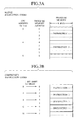
- the corresponding 16-bit instruction codes is stored in the addresses with low order four bits as 8h ⁇ Ah ⁇ Eh ⁇ 0h in this order. In the following description, it is assumed that the fifth bit of the address as counted from the least significant bit is 0 for the sake of clarity in explanation.
- the address as output from the processor 4 has low order four bits of 4h
- the corresponding 16-bit compressed instruction code is fetched from the address having low order four bits of 2h.
- the 16-bit compressed instruction code is converted by the instruction code conversion unit 3 into the corresponding 32-bit instruction code, which can be executed by the processor 4.
- the processor 4 executes the 32-bit instruction code followed by incrementing the address to be output to have low order four bits of 8h.
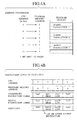
- variable-length codes there may be the case where a 32-bit compressed instruction code (instruction 2) in the addresses having low order four bits of 2h and low order four bits of 4h as illustrated in Fig.4.
- the processor 4 When the instruction 2 is to be fetched, the processor 4 outputs an address having low order four bits of 4h, which is shifted to the right and outputted to the program memory 1 as an address having low order four bits of 2h by means of the instruction code conversion unit 3 as illustrated in Fig.4(b).
- the instruction code conversion unit 3 then receives the high order 16 bits of the corresponding 32-bit compressed instruction code (the instruction 2) from the program memory 1.
- the instruction code conversion unit 3 When it is detected that the high order 16 bits is the high order 16 bits of a 32-bit compressed instruction code, the instruction code conversion unit 3 outputs a 32-bit "NOP" instruction which performs no operation.
- the processor 4 executes the 32-bit "NOP” instruction to increment the current addresses to have low order four bits of 8h. Then, the next 16 bits, i.e., the low 16 bits of the 32 bit compressed instruction code (the instruction 2) is fetched from the address having low order four bits of 4h which is generated by shifting the address having low order four bits of 8h to the right and given to the program memory 1.
- the 32-bit compressed instruction code thus obtained is converted into the corresponding 32-bit native instruction code (the instruction 2B') of the processor 4 and transferred to the processor 4 by means of the instruction code conversion unit 3.
- the processor 4 executes the 32-bit native instruction code 2B' and the current addresses is incremented to have low order four bits of Ch.
- the correspondence of the program memory address to the processor address is maintained simplified in this manner by executing a 32-bit "NOP" instruction.
- the simplification of the interrelation between the program memory address and the processor address makes it possible to dispense with correspondence information stored in the program memory 1 for the address conversion, as the sixth conventional example as described above, and therefore to reduce the time required for expanding the compressed instruction codes by the time which is otherwise required for reading and handling the address correspondence information.
- the address correspondence information is stored in the program memory so that the efficiency of coding is reduced.
- some instruction codes include operands each of which consists of a few low order bits indicative of necessary data and high order meaningless bits fixed to all 0 or all 1. It has therefore only little effect on the efficiency of coding that the compressed instruction code set is a subset of the original instruction set. Accordingly, in many cases, compilation by the use of compressed instruction codes can generate a size smaller than that generated by compilation by the use of native instruction codes. Needless to say, the compression is performed only for such a program or part of a program of which the compression is effective.
- the operands of many instruction codes can be represented by 1 to 8 bits.
- many native instruction codes include data fields of 16 bits and thereabout. Accordingly, a program may usually include a number of 32-bit native instruction codes each of which has redundancy of 15 to 8 bits. The redundancy bits are eliminated in the compressed instruction code set in order to improve the compression efficiency.
- the compression can be performed not only by compressing a 32-bit native instruction code to a compressed instruction code but also by compressing a plurality of native instruction codes to a smaller number of compressed instruction codes. For example, two native instruction codes can be compressed into one compressed instruction code in order to improve the compression efficiency.
- Fig.6 is a schematic diagram showing exemplary compressed instruction codes and the 32-bit native instruction codes which are obtained by expanding the exemplary compressed instruction codes.
- a compiler compiles a source text of the target program as written in a compiler language (a high level language such as C-language) to generate an assembler source text file consisting of native instruction codes of the subset.
- An assembler then converts the assembler source text file to a relocatable object file, which is then processed by a linker to generate an absolute object file consisting of native instruction codes.
- the above described absolute object file is furthermore processed by an object converter to a final object file in the hex form and the like.
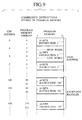
- the compressed instruction codes it is possible to design the compressed instruction codes to have the same bit length (fixed-length codes) or to have a plurality of bit lengths (variable-length codes).
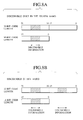
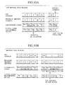
- variable-length codes there is an encoding method in which the bit length of an instruction is determined only by decoding high order bits, for example, by the use of part of the high order 16 bits of a 32-bit native instruction code for detecting the bit length thereof as illustrated in Fig.8(a).
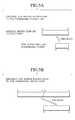
- the blocks are too large, there have to be provided a large buffer memory for storing the instructions as converted, resulting in an increase in costs.
- the execution time is influenced by the process of reading and converting a large block at a time.
- the buffer size is determined, taking into consideration the tradeoff made therebetween.
- the processor 4 is designed to execute fixed-length 32-bit instruction codes C1, C2, C3 ⁇ .
- a compressed instruction code set of 16-bit and 32-bit variable-length codes A1, A2, A3 ⁇ is provided as the compressed instruction codes for improving the efficiency of coding.
- the compressed instruction codes are generated by a software as described above as an object file. It is assumed that part of the program source is not compressed.
- a furthermore alternative is the use of an MMU (Memory Management Unit).
- property registers are provided for storing property values in correspondence with the addresses as outputted from the processor 4.
- the property values are used for indicating whether the instruction of the current address is a compressed instruction or a native instruction.
- the property value stored in the property register can be set by the input/output instruction of the processor 4. It is possible to make use of external signals for the purpose of determining whether the instruction of the current address is a compressed instruction or a native instruction. For example, in the case where a plurality of program memories are provided, each program memory is given a property indicative that it is responsible for storing compressed instruction codes or native instruction codes.
- the instruction code conversion unit 3 can distinguish between the compressed instruction codes and the native instruction codes by the property of the program memory currently accessed.
- the signal outputted from the processor 4 for fetching instructions depends upon the architecture of the processor. In the cases other than the Harvard Architecture, the processor 4 outputs a signal indicative of if it is either data or an instruction which is accessed together with a signal indicative of reading and an address signal. However, if the request signal for fetching instruction is separated from the request signal for fetching data, there is no need for the signal indicative of if it is either data or an instruction which is accessed. Also, in the case where separate memories are provided respectively for storing a program and for storing data, it can be determined whether or not the memory access is conducted to fetch an instruction by decoding the address signal so that there is no need for the signal indicative of if it is either data or an instruction which is accessed. In this example, the range of addresses is used for determining whether or not the memory access is conducted to fetch an instruction.
- the compressed instruction code is expanded to the corresponding 32-bit native instruction code. For example, if the compressed instruction code located in the top of the block is a 16-bit instruction code, it is immediately expanded to a 32-bit native instruction code. If the compressed instruction code located in the top of the block is a 32-bit native instruction code, the high order 16 bits of the compressed instruction code is read out from the top address of the program memory 1 followed by detecting the bit length of 32 bits.
- the instruction code conversion unit 3 After transferring the native instruction code to the processor 4, the instruction code conversion unit 3 continues to sequentially read and expand compressed instruction codes and to store the native instruction codes. However, when an exception occurrs such as an interrupt request or the processor 4 executes a branch instruction so that the output address from the processor 4 is out of the block, the instruction code conversion unit 3 halts the expansion of compressed instruction codes of the block and immediately initiate the expansion of compressed instruction codes of a new block to which the control is transferred. The time of the expansion is thereby prevented from being elongated by this control. However, the control may be transferred to the remote address after completing the expansion process of the compressed instruction codes having already been fetched from the program memory. Meanwhile, if there is repeated a loop bridging adjacent blocks, the expansion process of the same block is repeated.
- the addresses as output from the processor 4 is transferred to the memory interface 2 without conversion followed by reading the corresponding native instruction code from the program memory 1.
- the native instruction code as read out is transferred to the processor 4 as it is.
- the addresses as output from the processor 4 is transferred to the memory interface 2 without conversion followed by reading data from or writing data to the program memory 1.
- the control is sometimes transferred from a certain block for which the expansion process has been conducted to another block by an exception or a branch instruction which is located in the middle or the last address of the certain block, and then returned to the certain block.
- the program memory 1 need not be accessed from the top address thereof, but native instruction codes can be read from the buffer memory which accommodates native instruction codes of two blocks. The response time of the instruction code conversion unit 3 can be thereby improved.
- the instruction code conversion unit 3 can output native instruction codes stored in the buffer memory while subsequent compressed instruction codes are read out from the program memory, expanded and stored in the buffer memory.
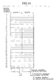
- the buffer memory designation register serves to which block of the buffer memory should be used next as illustrated in Fig.14.
- the buffer memory designation register is a one-bit register which serves to indicate the use of the buffer memory block 0 if "0" is set thereto and indicate the use of the buffer memory block 1 if "1" is set therein. Any buffer memory block can be used when the system is reset so that the initialization process of the buffer memory designation register can be dispensed with.
- the buffer memory designation register indicates the use of another block.
- the buffer memory designation register is controlled to indicate the use of the block storing older instructions.
- the bandwidth of the memory interface becomes wider so that the time required for reading the memory, when expanding compressed instruction codes, can be reduced by fetching a plurality of compressed instruction codes at a time, resulting in a shorter time required for the expansion process.
- a secondary cache memory or a primary cache memory can be used resulting in the advantage in costs and in the time for fetching instructions.
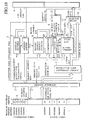
- the information processing system is composed of the program memory 1 which may be composed of a plurality of memory chips in which are stored a plurality of the 16-bit fixed compressed instruction codes A1, A2, A3 ⁇ and the fixed-length 32-bit native instruction codes B1, B2, B3 ⁇ , the memory interface 2 for reading the compressed instruction codes from the program memory 1, the instruction code conversion unit 3 for converting the compressed instruction codes to the native instruction codes and the processor (CPU) 4 serves to execute the fixed-length 32-bit native instruction codes.
- the instruction code conversion unit 3 is composed of an address decoder 5, an address shifter 6, an instruction code conversion circuit 7, a buffer memory 8, block address storing register 9, comparator circuit 10, a selector circuit 11, a memory read request control circuit 12 and a control circuit 13.
- the address decoder 5 serves to decode an processor address CA4 as outputted from the processor 4, determine whether the processor address CA4 falls in the compressed instruction code address range or the native instruction code address range and output a compressed/native instruction discrimination signal S5.
- the control circuit 13 serves to generate a writing signal S13a for initializing the valid bits and writing an appropriate address on the block address storing register 9 and a writing signal S13b for writing the valid bit of the buffer memory 8 corresponding to the low order bits of the output address from the address shifter 6 in accordance with the compressed/native instruction discrimination signal S5 as the decoding result of the address decoder 5, the memory read request signal S12 as the output signal of the memory read request control circuit 12, the matching signal S10 as the output of the comparator 10.
- the address range of the compressed instruction codes A1, A2, A3 ⁇ and the address range of the compressed instruction codes B1, B2, B3 ⁇ are distinguished by the processor address CA4 as output from the processor 4.
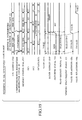
- compressed instruction codes A1, A2, A3, A4 ⁇ are stored in the addresses from 00000900h while native instruction codes B1, B2, B3 ⁇ are stored in the addresses from 40000000h in advance.
- the processor 4 When executing the instruction code C2, the processor 4 increments the address to 00001208h. If the instruction code C2 is such an instruction which changes the flow of the program, e.g., a branch instruction, an exception invoking instruction and so forth, the processor 4 outputs the destination address and the like as the next address.
- the compressed instruction codes A3 as read from the address of 00001208h is converted into the instruction code C3, which is then executed by the processor 4, in the same sequence as from the address of 00001204h.
- the processor 4 increments the processor address CA4 by +4 from the address of 40000000h to the address of 40000004h.
- the instruction code B2 as read from the address of 40000004h is transferred to the processor 4 and then executed by the processor 4, in the same sequence as from the address of 40000000h. In this manner, since only native instruction codes are transferred to the processor 4, it is not necessary to modify the hardware of the processor.
- an instruction code inverse conversion circuit in the instruction code conversion unit 3 for performing compression i.e., a native instruction code as given is converted into the corresponding compressed instruction code
- the bit length of a compressed instruction is determined by decoding the high order 6 bits of the high order 16 bits of a 32-bit compressed instruction code or the high order 6 bits of a 16-bit compressed instruction code. For example, the bit length of a compressed instruction is determined as 32 bits when the high 6 bits is 000000b to 000011b or 010011b (binary number) and as 16 bits when the high 6 bits is 000100b to 010010b of 011000b.
- Exemplary compressed instruction codes and the 32-bit native instruction codes which are obtained by expanding the exemplary compressed instruction codes are as illustrated in Fig.6.
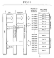
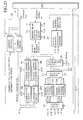
- the instruction code conversion unit 30 is provided further with an address generator 14, selector circuits 17, 20 and 22, control circuits 21 and 23, a selector circuit 25, comparator circuits 26, 10a and 10b, high order bits storing registers 16a and 16b, a code length detection circuit 18, code length storing circuits 19a and 19b, effective address storing registers 24a and 24b and a buffer memory designation register 27.
- the address generator 14 serves to generate an address MA14 to be transferred to the memory interface 2.
- the selector circuit 17 serves to select the contents of the high order bits storing registers 16a and 16b in accordance with the output signal S27 of the buffer memory designation register 27.
- the selector circuit 20 serves to select the contents of the code length storing circuits 19a and 19b in accordance with the output signal S27 of the buffer memory designation register 27.
- the selector circuit 22 serves to select the contents of the buffer memory blocks 8a and 8b in accordance with the output signal S27 of the buffer memory designation register 27.
- the control circuit 21 serves to generate a selection signal S21 given to the selector circuit 11 and the control circuit 15 which serves to generate the writing signals S15a and S15b of the high order bits storing registers 16a and 16b.
- the comparator circuits 10a and 10b serves to compare the addresses BA9a and BA9b contained in the block address storing registers 9a and 9b with the high order bits of the address MA6 to determine matching therebetween.
- the high order bits storing registers 16a and 16b serves to store the instruction code OC2 read through the memory interface 2 in the case where the instruction code OC2 is the high order 16 bits of a 32-bit compressed instruction code.
- the code length detection circuit 18 serves to detect if the instruction code OC2 read through the memory interface 2 is the high order 16 bits of a 32-bit compressed instruction code.
- the code length storing circuits 19a and 19b serves to store the information of whether the instruction code OC2 read through the memory interface 2 is a 16-bit instruction code or a 32-bit instruction code.
- the effective address storing registers 24a and 24b are indicative of the addresses of the buffer memory blocks 8a and 8b to which address expanded instruction codes are stored in the buffer memory block from the top addresses respectively.
- the buffer memory designation register 27 serves to which buffer memory block 8a or 8b should be used next.
- the effective address storing register 24a or 24b serves to indicate, if it is set to "0", that no valid native instruction code is stored in the buffer memory block 8a or 8b, and is incremented by +2 in response to the counting up signal S23c or S23d as described above.
- the top address of said block is set to either the block address storing register 9a or 9b which is selected by the buffer memory designation register 27 while either the effective address storing register 24a or 24b which is also selected by the buffer memory designation register 27 is cleared to "0".
- the code length detection circuit 18 then decodes the high order 6 bits of the compressed instruction code as read out in order that judge whether the bit length of the compressed instruction codes is 16 bits or 32 bits.
- the result of judgment is set to the code length storing circuit 19a or 19b which is selected by the buffer memory designation register 27.
- the result of judgment is 00b (binary number) in the case of 16 bits and 10b (binary number) in the case of 32 bits.
- the instruction code conversion circuit 7 serves to combine the high order 16 bits of the 32-bit compressed instruction code as read out first with the low order 16 bits thereof as read out latter, convert the 32-bit compressed instruction code in combination into at least two 32-bit native instruction codes (either pair of DH1/DL1, DH2/DL2, DH3/DL3 ⁇ ) and store the two 32-bit native instruction codes in the buffer memory block 8a or 8b which is selected by the buffer memory designation register 27.
- the effective address storing register 24a or 24b which is selected by the buffer memory designation register 27 is incremented by +4.
- the compressed instruction code as required by the processor 4 has been read out from the program memory 1 through the memory interface 2, converted into the corresponding native instruction codes by means of the instruction code conversion circuit 7 and stored in the buffer memory block 8a or 8b.
- the compressed instruction code as required by the processor 4 is then is transferred to the processor 4 from the instruction code conversion circuit 7 for execution. While the native instruction code is executed, the compressed instruction codes of the current block are continuously read out from the program memory 1, converted into the corresponding native instruction codes, and stored in the buffer memory block 8a or 8b.
- the processor address CA4 is updated.
- the content of the block address storing register 9a or 9b is compared with the high order bits (other than the low order 6 bits) of the processor address shifted to the right by the address shifter 6 for the purpose of determining whether or not the processor address CA4 falls in a block of which part or all of the instruction codes have been converted. Namely, if the result of comparison indicates a match, it is determined that the processor address CA4 falls in the block followed by storing a value to the buffer memory designation register 27 in order to indicate one of the buffer memory blocks 8a and 8b corresponding to the match. If the result of comparison indicates no match, it is determined that the processor address CA4 points an address outside of the block followed by storing a value to the buffer memory designation register 27 in order to indicate one of the buffer memory blocks 8a and 8b other than that is lastly used.
- the 32-bit "NOP" instruction code is stored in the address 04h of the buffer memory block 8a or 8b while the 32-bit instruction code DL1 is stored in the address 08h of the buffer memory block 8a or 8b.
- bit length information indicative of whether the bit length of the compressed instruction codes is 16 bits or 32 bits.
- bit length information of 32 bits are provided for each block in order that a "0" bit is provided for a 16-bit compressed instruction code and the high order 16 bits of a 32-bit compressed instruction code while a "1" bit is provided for the low order 16 bits of a 32-bit compressed instruction code.
- bit length information is recognized part of an instruction code
- this technique is recognized as the above described encoding method in which the bit length of an instruction is determined by decoding any part of a 32-bit native instruction code as fetched as illustrated in Fig.8(b).
- Such system applications of the present invention as requiring reduction in memory capacity include the system requiring a memory capacity larger than the inherent memory space of the processor.
- An example of such processors of this kind is a processor which has an internal memory space of 32 bits but only has a 28-bit address bus. In this case, a program requiring an address space exceeding 28 bits may be implemented within the address space of 28 bits by the use of compression.
Landscapes
- Engineering & Computer Science (AREA)
- Software Systems (AREA)
- Theoretical Computer Science (AREA)
- Physics & Mathematics (AREA)
- General Engineering & Computer Science (AREA)
- General Physics & Mathematics (AREA)
- Executing Machine-Instructions (AREA)
Applications Claiming Priority (2)
| Application Number | Priority Date | Filing Date | Title |
|---|---|---|---|
| JP2000030948A JP3556556B2 (ja) | 2000-02-08 | 2000-02-08 | 命令コード変換装置及び情報処理システム |
| JP2000030948 | 2000-02-08 |
Publications (3)
| Publication Number | Publication Date |
|---|---|
| EP1124180A2 true EP1124180A2 (fr) | 2001-08-16 |
| EP1124180A3 EP1124180A3 (fr) | 2003-05-02 |
| EP1124180B1 EP1124180B1 (fr) | 2015-11-04 |
Family
ID=18555890
Family Applications (1)
| Application Number | Title | Priority Date | Filing Date |
|---|---|---|---|
| EP01301062.4A Expired - Lifetime EP1124180B1 (fr) | 2000-02-08 | 2001-02-07 | Système de traitement de données avec conversion de code d'instruction et procédé pour la génération d'instructions |
Country Status (3)
| Country | Link |
|---|---|
| US (1) | US6801996B2 (fr) |
| EP (1) | EP1124180B1 (fr) |
| JP (1) | JP3556556B2 (fr) |
Cited By (1)
| Publication number | Priority date | Publication date | Assignee | Title |
|---|---|---|---|---|
| CN107562442A (zh) * | 2017-09-22 | 2018-01-09 | 广州酷狗计算机科技有限公司 | 一种读取数据的方法和装置 |
Families Citing this family (38)
| Publication number | Priority date | Publication date | Assignee | Title |
|---|---|---|---|---|
| US7028286B2 (en) * | 2001-04-13 | 2006-04-11 | Pts Corporation | Methods and apparatus for automated generation of abbreviated instruction set and configurable processor architecture |
| JP2003108367A (ja) * | 2001-09-27 | 2003-04-11 | Yamaha Corp | プログラムメモリ削減方法およびプログラムメモリ読出回路 |
| US7278137B1 (en) * | 2001-12-26 | 2007-10-02 | Arc International | Methods and apparatus for compiling instructions for a data processor |
| US6912649B2 (en) * | 2002-03-13 | 2005-06-28 | International Business Machines Corporation | Scheme to encode predicted values into an instruction stream/cache without additional bits/area |
| US7398276B2 (en) * | 2002-05-30 | 2008-07-08 | Microsoft Corporation | Parallel predictive compression and access of a sequential list of executable instructions |
| US6907516B2 (en) * | 2002-05-30 | 2005-06-14 | Microsoft Corporation | Compression of program instructions using advanced sequential correlation |
| GB2400198B (en) * | 2003-04-04 | 2006-04-05 | Advanced Risc Mach Ltd | Controlling execution of a block of program instructions within a computer processing system |
| GB2402763B (en) * | 2003-06-13 | 2006-03-01 | Advanced Risc Mach Ltd | Data access program instruction encoding |
| US20040252687A1 (en) * | 2003-06-16 | 2004-12-16 | Sridhar Lakshmanamurthy | Method and process for scheduling data packet collection |
| TWI224281B (en) * | 2003-07-16 | 2004-11-21 | Sunplus Technology Co Ltd | A processor executing script with different length and method thereof |
| WO2005103922A2 (fr) * | 2004-03-26 | 2005-11-03 | Atmel Corporation | Systeme sur puce a processeur de signaux numeriques a virgule flottante comprenant un domaine complexe a processeur double |
| US7278122B2 (en) * | 2004-06-24 | 2007-10-02 | Ftl Systems, Inc. | Hardware/software design tool and language specification mechanism enabling efficient technology retargeting and optimization |
| US7676799B1 (en) * | 2005-06-10 | 2010-03-09 | Sun Microsystems, Inc. | Address simplification by binary transformation |
| US20070226724A1 (en) * | 2006-03-24 | 2007-09-27 | Mediatek Inc. | Method and apparatus for firmware execution and provision |
| CN101398752B (zh) * | 2007-09-29 | 2011-08-31 | 国际商业机器公司 | 重叠指令存取单元和重叠指令存取方法 |
| US20100023733A1 (en) * | 2008-04-15 | 2010-01-28 | Vns Portfolio Llc | Microprocessor Extended Instruction Set Precision Mode |
| WO2010116735A1 (fr) * | 2009-04-10 | 2010-10-14 | パナソニック株式会社 | Dispositif de mémoire cache, procédé de commande de mémoire cache, programme et circuit intégré |
| US20110072238A1 (en) * | 2009-09-20 | 2011-03-24 | Mimar Tibet | Method for variable length opcode mapping in a VLIW processor |
| WO2012103367A2 (fr) | 2011-01-27 | 2012-08-02 | Soft Machines, Inc. | Mappages d'adresses de blocs invité-natives et gestion du stockage des codes natifs |
| WO2012103253A2 (fr) | 2011-01-27 | 2012-08-02 | Soft Machines, Inc. | Mémoire cache de table de conversion multiniveau permettant de traduire des instructions d'hôte en instructions d'origine |
| WO2012103373A2 (fr) | 2011-01-27 | 2012-08-02 | Soft Machines, Inc. | Structure de mise en cache variable pour la gestion d'un stockage physique |
| WO2012103245A2 (fr) | 2011-01-27 | 2012-08-02 | Soft Machines Inc. | Bloc d'instructions d'hôte doté d'une construction en séquence de sauts proches et de sauts éloignés vers un bloc d'instructions d'origine |
| WO2012103209A2 (fr) | 2011-01-27 | 2012-08-02 | Soft Machines, Inc. | Mappage basé sur une plage d'instructions hôtes à instructions natives au moyen de la mémoire cache conversion look aside buffer d'un processeur |
| WO2012103359A2 (fr) | 2011-01-27 | 2012-08-02 | Soft Machines, Inc. | Composants d'accélération matérielle pour traduire des instructions invité en instructions natives |
| US9201652B2 (en) | 2011-05-03 | 2015-12-01 | Qualcomm Incorporated | Methods and apparatus for storage and translation of entropy encoded software embedded within a memory hierarchy |
| US10120692B2 (en) | 2011-07-28 | 2018-11-06 | Qualcomm Incorporated | Methods and apparatus for storage and translation of an entropy encoded instruction sequence to executable form |
| US20140115304A1 (en) * | 2012-10-18 | 2014-04-24 | Synopsys, Inc. | Compressed instruction code storage |
| TWI584197B (zh) * | 2013-01-25 | 2017-05-21 | 凌通科技股份有限公司 | 程式碼之動態產生系統及其方法 |
| EP2972798B1 (fr) | 2013-03-15 | 2020-06-17 | Intel Corporation | Procédé et appareil pour une émulation de pile d'adresses de retour d'hôte prenant en charge une spéculation |
| WO2014151652A1 (fr) | 2013-03-15 | 2014-09-25 | Soft Machines Inc | Procédé et appareil pour permettre une résolution précoce des dépendances et un envoi de données dans un microprocesseur |
| JP2015049832A (ja) | 2013-09-04 | 2015-03-16 | インターナショナル・ビジネス・マシーンズ・コーポレーションInternational Business Machines Corporation | 定数ロードのオーバーヘッドを削減する方法、装置及びプログラム |
| US9372696B2 (en) * | 2013-10-18 | 2016-06-21 | Via Technologies, Inc. | Microprocessor with compressed and uncompressed microcode memories |
| KR102143521B1 (ko) | 2014-04-21 | 2020-08-11 | 삼성전자 주식회사 | 불휘발성 메모리 시스템, 이를 포함하는 메모리 카드 및 불휘발성 메모리 시스템의 동작방법 |
| US9910787B2 (en) | 2014-06-05 | 2018-03-06 | Micron Technology, Inc. | Virtual address table |
| US9928066B2 (en) * | 2015-06-25 | 2018-03-27 | Intel Corporation | Instruction and logic for encoded word instruction compression |
| US10621353B2 (en) * | 2016-12-28 | 2020-04-14 | Intel Corporation | Firmware loading for exploit resistance |
| CN116466995B (zh) * | 2023-06-16 | 2024-06-11 | 紫光同芯微电子有限公司 | 基于复合指令的指令及其操作数的优化方法及装置 |
| CN117118570B (zh) * | 2023-09-06 | 2024-04-02 | 上海交通大学 | 有限位数的最大码距遥控指令码生成系统及方法 |
Citations (2)
| Publication number | Priority date | Publication date | Assignee | Title |
|---|---|---|---|---|
| EP0324308A2 (fr) | 1988-01-11 | 1989-07-19 | International Business Machines Corporation | Méthode et système de décodage d'instructions de plusieurs formats incompatibles |
| US5881258A (en) | 1997-03-31 | 1999-03-09 | Sun Microsystems, Inc. | Hardware compatibility circuit for a new processor architecture |
Family Cites Families (14)
| Publication number | Priority date | Publication date | Assignee | Title |
|---|---|---|---|---|
| JPH0520086A (ja) | 1991-07-11 | 1993-01-29 | Nec Corp | 数値演算処理装置 |
| AU2939892A (en) * | 1991-12-06 | 1993-06-28 | Richard S. Norman | Massively-parallel direct output processor array |
| JPH06348490A (ja) | 1993-06-08 | 1994-12-22 | Hitachi Ltd | 演算処理方法、及びマイクロコンピュータ |
| JPH0962504A (ja) | 1995-08-23 | 1997-03-07 | Oki Electric Ind Co Ltd | 命令処理装置 |
| US6151618A (en) * | 1995-12-04 | 2000-11-21 | Microsoft Corporation | Safe general purpose virtual machine computing system |
| KR100466722B1 (ko) * | 1996-01-24 | 2005-04-14 | 선 마이크로시스템즈 인코퍼레이티드 | 어레이경계검사방법및장치와,이를포함하는컴퓨터시스템 |
| JP3201716B2 (ja) | 1996-02-22 | 2001-08-27 | シャープ株式会社 | コンピュータ装置 |
| EP0941508B1 (fr) * | 1997-10-02 | 2007-01-17 | Koninklijke Philips Electronics N.V. | Ordinateur a ensembles d'instructions variables |
| US6529635B1 (en) * | 1997-12-15 | 2003-03-04 | Intel Corporation | Shape-based image compression/decompression using pattern matching |
| JPH11306015A (ja) | 1998-04-22 | 1999-11-05 | Matsushita Electric Ind Co Ltd | 演算処理方法及びそれを用いたマイクロコンピュータ |
| US6141635A (en) * | 1998-06-12 | 2000-10-31 | Unisys Corporation | Method of diagnosing faults in an emulated computer system via a heterogeneous diagnostic program |
| US6128094A (en) * | 1998-07-08 | 2000-10-03 | Hewlett-Packard Company | Printer having processor with instruction cache and compressed program store |
| US6397324B1 (en) * | 1999-06-18 | 2002-05-28 | Bops, Inc. | Accessing tables in memory banks using load and store address generators sharing store read port of compute register file separated from address register file |
| JP2001195250A (ja) | 2000-01-13 | 2001-07-19 | Mitsubishi Electric Corp | 命令トランスレータ、トランスレータ付命令メモリおよびそれらを用いたデータ処理装置 |
-
2000
- 2000-02-08 JP JP2000030948A patent/JP3556556B2/ja not_active Expired - Fee Related
-
2001
- 2001-02-07 US US09/778,069 patent/US6801996B2/en not_active Expired - Lifetime
- 2001-02-07 EP EP01301062.4A patent/EP1124180B1/fr not_active Expired - Lifetime
Patent Citations (2)
| Publication number | Priority date | Publication date | Assignee | Title |
|---|---|---|---|---|
| EP0324308A2 (fr) | 1988-01-11 | 1989-07-19 | International Business Machines Corporation | Méthode et système de décodage d'instructions de plusieurs formats incompatibles |
| US5881258A (en) | 1997-03-31 | 1999-03-09 | Sun Microsystems, Inc. | Hardware compatibility circuit for a new processor architecture |
Cited By (2)
| Publication number | Priority date | Publication date | Assignee | Title |
|---|---|---|---|---|
| CN107562442A (zh) * | 2017-09-22 | 2018-01-09 | 广州酷狗计算机科技有限公司 | 一种读取数据的方法和装置 |
| CN107562442B (zh) * | 2017-09-22 | 2020-03-17 | 广州酷狗计算机科技有限公司 | 一种读取数据的方法和装置 |
Also Published As
| Publication number | Publication date |
|---|---|
| US6801996B2 (en) | 2004-10-05 |
| US20010013093A1 (en) | 2001-08-09 |
| EP1124180A3 (fr) | 2003-05-02 |
| EP1124180B1 (fr) | 2015-11-04 |
| JP2001222426A (ja) | 2001-08-17 |
| JP3556556B2 (ja) | 2004-08-18 |
Similar Documents
| Publication | Publication Date | Title |
|---|---|---|
| EP1124180B1 (fr) | Système de traitement de données avec conversion de code d'instruction et procédé pour la génération d'instructions | |
| KR0185988B1 (ko) | 멀티프로세서 또는 파이프 라인식 프로세서 시스템에서 데이타의 보존을 확실히 하는 방법 | |
| US5561775A (en) | Parallel processing apparatus and method capable of processing plural instructions in parallel or successively | |
| US8893079B2 (en) | Methods for generating code for an architecture encoding an extended register specification | |
| KR100535852B1 (ko) | 데이타처리장치 | |
| US20090138685A1 (en) | Processor for processing instruction set of plurality of instructions packed into single code | |
| US20070106889A1 (en) | Configurable instruction sequence generation | |
| JP2006185462A (ja) | 高データ密度のriscプロセッサ | |
| US20010010072A1 (en) | Instruction translator translating non-native instructions for a processor into native instructions therefor, instruction memory with such translator, and data processing apparatus using them | |
| CN112667289B (zh) | 一种cnn推理加速系统、加速方法及介质 | |
| KR20010043772A (ko) | 혼합 벡터/스칼라 레지스터 파일 | |
| KR19980032264A (ko) | 벡터 프로세서 프로그래밍 및 벡터 프로세서와 risc 프로세서를 구비하는 비대칭 이중 프로세서의 병렬 프로그래밍 | |
| JP2007234048A (ja) | コード圧縮技術の高速プロトタイピングを可能にするプログラムのコード圧縮方法、プログラムのコード圧縮システム | |
| CN103748550B (zh) | 用于存储熵编码指令序列及将其翻译成可执行形式的方法和设备 | |
| US20080201564A1 (en) | Data processor | |
| JPH1049368A (ja) | 条件実行命令を有するマイクロプロセッサ | |
| JP2001034471A (ja) | Vliw方式プロセッサ | |
| EP0036093A2 (fr) | Système de traitement d'information composé d'une unité de commande arithmétique formée sur une seule puce par application d'un circuit semiconducteur à haute intégration | |
| US7581082B2 (en) | Software source transfer selects instruction word sizes | |
| CN104216682B (zh) | 微处理器以及选择性解压缩微程序码的相关方法 | |
| KR100867564B1 (ko) | 프로그램 제어 흐름에서 변경들을 이루기 위한 장치 및 방법 | |
| JP4502532B2 (ja) | データ処理装置 | |
| US6564316B1 (en) | Method and apparatus for reducing code size by executing no operation instructions that are not explicitly included in code using programmable delay slots | |
| US5212779A (en) | System for guarantee reexecution after interruption by conditionally used store buffer if microinstruction being executed is a memory write and last microinstruction | |
| US6877082B1 (en) | Central processing unit including address generation system and instruction fetch apparatus |
Legal Events
| Date | Code | Title | Description |
|---|---|---|---|
| PUAI | Public reference made under article 153(3) epc to a published international application that has entered the european phase |
Free format text: ORIGINAL CODE: 0009012 |
|
| 17P | Request for examination filed |
Effective date: 20010215 |
|
| AK | Designated contracting states |
Kind code of ref document: A2 Designated state(s): AT BE CH CY DE DK ES FI FR GB GR IE IT LI LU MC NL PT SE TR |
|
| AX | Request for extension of the european patent |
Free format text: AL;LT;LV;MK;RO;SI |
|
| PUAL | Search report despatched |
Free format text: ORIGINAL CODE: 0009013 |
|
| AK | Designated contracting states |
Designated state(s): AT BE CH CY DE DK ES FI FR GB GR IE IT LI LU MC NL PT SE TR |
|
| AX | Request for extension of the european patent |
Extension state: AL LT LV MK RO SI |
|
| RIC1 | Information provided on ipc code assigned before grant |
Ipc: 7G 06F 9/38 B Ipc: 7G 06F 9/318 A |
|
| AKX | Designation fees paid |
Designated state(s): DE FR GB |
|
| 17Q | First examination report despatched |
Effective date: 20081230 |
|
| GRAP | Despatch of communication of intention to grant a patent |
Free format text: ORIGINAL CODE: EPIDOSNIGR1 |
|
| INTG | Intention to grant announced |
Effective date: 20150520 |
|
| GRAS | Grant fee paid |
Free format text: ORIGINAL CODE: EPIDOSNIGR3 |
|
| GRAA | (expected) grant |
Free format text: ORIGINAL CODE: 0009210 |
|
| AK | Designated contracting states |
Kind code of ref document: B1 Designated state(s): DE FR GB |
|
| REG | Reference to a national code |
Ref country code: GB Ref legal event code: FG4D |
|
| REG | Reference to a national code |
Ref country code: DE Ref legal event code: R096 Ref document number: 60149650 Country of ref document: DE |
|
| REG | Reference to a national code |
Ref country code: FR Ref legal event code: PLFP Year of fee payment: 16 |
|
| PGFP | Annual fee paid to national office [announced via postgrant information from national office to epo] |
Ref country code: DE Payment date: 20160202 Year of fee payment: 16 |
|
| PGFP | Annual fee paid to national office [announced via postgrant information from national office to epo] |
Ref country code: GB Payment date: 20160203 Year of fee payment: 16 Ref country code: FR Payment date: 20160108 Year of fee payment: 16 |
|
| REG | Reference to a national code |
Ref country code: DE Ref legal event code: R097 Ref document number: 60149650 Country of ref document: DE |
|
| PLBE | No opposition filed within time limit |
Free format text: ORIGINAL CODE: 0009261 |
|
| STAA | Information on the status of an ep patent application or granted ep patent |
Free format text: STATUS: NO OPPOSITION FILED WITHIN TIME LIMIT |
|
| 26N | No opposition filed |
Effective date: 20160805 |
|
| REG | Reference to a national code |
Ref country code: DE Ref legal event code: R119 Ref document number: 60149650 Country of ref document: DE |
|
| GBPC | Gb: european patent ceased through non-payment of renewal fee |
Effective date: 20170207 |
|
| REG | Reference to a national code |
Ref country code: FR Ref legal event code: ST Effective date: 20171031 |
|
| PG25 | Lapsed in a contracting state [announced via postgrant information from national office to epo] |
Ref country code: DE Free format text: LAPSE BECAUSE OF NON-PAYMENT OF DUE FEES Effective date: 20170901 Ref country code: FR Free format text: LAPSE BECAUSE OF NON-PAYMENT OF DUE FEES Effective date: 20170228 |
|
| PG25 | Lapsed in a contracting state [announced via postgrant information from national office to epo] |
Ref country code: GB Free format text: LAPSE BECAUSE OF NON-PAYMENT OF DUE FEES Effective date: 20170207 |