EP0324407A2 - Procédé d'ajustage par rayon laser - Google Patents
Procédé d'ajustage par rayon laser Download PDFInfo
- Publication number
- EP0324407A2 EP0324407A2 EP89100264A EP89100264A EP0324407A2 EP 0324407 A2 EP0324407 A2 EP 0324407A2 EP 89100264 A EP89100264 A EP 89100264A EP 89100264 A EP89100264 A EP 89100264A EP 0324407 A2 EP0324407 A2 EP 0324407A2
- Authority
- EP
- European Patent Office
- Prior art keywords
- trimmed
- laser
- trimming process
- region
- laser beam
- Prior art date
- Legal status (The legal status is an assumption and is not a legal conclusion. Google has not performed a legal analysis and makes no representation as to the accuracy of the status listed.)
- Granted
Links
Images


Classifications
-
- H—ELECTRICITY
- H01—ELECTRIC ELEMENTS
- H01C—RESISTORS
- H01C17/00—Apparatus or processes specially adapted for manufacturing resistors
- H01C17/22—Apparatus or processes specially adapted for manufacturing resistors adapted for trimming
- H01C17/24—Apparatus or processes specially adapted for manufacturing resistors adapted for trimming by removing or adding resistive material
- H01C17/242—Apparatus or processes specially adapted for manufacturing resistors adapted for trimming by removing or adding resistive material by laser
-
- H—ELECTRICITY
- H10—SEMICONDUCTOR DEVICES; ELECTRIC SOLID-STATE DEVICES NOT OTHERWISE PROVIDED FOR
- H10D—INORGANIC ELECTRIC SEMICONDUCTOR DEVICES
- H10D1/00—Resistors, capacitors or inductors
- H10D1/40—Resistors
- H10D1/47—Resistors having no potential barriers
- H10D1/474—Resistors having no potential barriers comprising refractory metals, transition metals, noble metals, metal compounds or metal alloys, e.g. silicides
-
- H—ELECTRICITY
- H10—SEMICONDUCTOR DEVICES; ELECTRIC SOLID-STATE DEVICES NOT OTHERWISE PROVIDED FOR
- H10P—GENERIC PROCESSES OR APPARATUS FOR THE MANUFACTURE OR TREATMENT OF DEVICES COVERED BY CLASS H10
- H10P34/00—Irradiation with electromagnetic or particle radiation of wafers, substrates or parts of devices
- H10P34/40—Irradiation with electromagnetic or particle radiation of wafers, substrates or parts of devices with high-energy radiation
- H10P34/42—Irradiation with electromagnetic or particle radiation of wafers, substrates or parts of devices with high-energy radiation with electromagnetic radiation, e.g. laser annealing
Definitions
- the present invention relates to a trimming process for trimming a thin film resistor, for example, by a laser beam.
- the trimming process by a laser beam allows an operator to trim or delineate an integrated circuit on a chip without any electrical contact with the integrated circuit.
- a major factor to determine the output characteristics of the integrated circuit is, for example, a resistance of a resistor of an integrated circuit
- a proper resistance is initially set up, the integrated circuit is operated, and a resistance of the resistor is finely adjusted by cutting or trimming it by a laser beam till a desired resistance is obtained, while observing the output characteristics. This process is called a functional laser trimming process.
- the process for adjusting a resistance of a resistor comes in two varieties.
- a first resistance adjusting process the resistance is adjusted by changing the direction of the lines of electric force.
- a resistive film is groove worked.
- a resistor network consisting of a plurality of resistor elements is used.
- the resistor network is partially cut off to change a connection in the network.
- FIG. 1A A conceptual illustration of a power distribution of an irradiating laser beam is given in Fig. 1A.
- an abscissa of the graph represents an extension of a beam spot in the radial direction.
- An ordinate represents a power of the laser beam spot.
- the beam spot is moved in the direction orthogonal to a plane of the drawing.
- a distribution of the laser power is a Gaussian distribution in which a peak power exists at point A as the center of the beam spot, and the peak power gradually decreases toward the peripheral side of the beam spot.
- 1B shows a state of a trimmed workpiece or material 1 when it is irradiated with a laser beam.
- trimmed material 1 absorbs energy of the laser beam.
- the absorbed laser energy is converted into a corresponding thermal energy, so that trimmed material 1 is heated.
- Portion 1a distanced from the center of the laser beam spot is a solidus region where is heated by the thermal energy resulting from the absorbed laser energy.
- An amount of heat value increases toward the center of the laser beam, and a melting point of the trimmed material is reached to form melting region 1b.
- an object of the present invention is to provide a trimming process by which no protruded portion is formed at the fringe of the trimmed portion of a trimmed material when it is trimmed, and a protecting film covering a substrate maintains its reliability for a long time after the trimming process is completed.
- a trimming process by a laser beam comprising the steps of: forming a laser shield layer over an untrimmed region of a trimmed material adjacent to a trimmed region, the laser shield layer having a higher heat conductivity than the trimmed material and a large reflectivity for laser beam; and cutting off the trimmed material by applying a laser beam onto the upper surface of the trimmed region of the trimmed material and vaporizing the trimmed material in the trimmed region.
- the laser shield layer is also subjected to the laser beam.
- the laser beam applied to the laser shield layer is weaker than that at the center of the laser spot. Additionally, the shield layer has a large reflectivity. Therefore, an amount of the laser energy absorbed directly by the laser shield layer is small.
- the trimmed material in the untrimmed region is shielded from the laser beam by means of the laser shield layer, but is heated by the heat transferred from the cut-off region. It is noted here that a heat conductivity of the laser shield layer is good, and therefore most of the heat from the cut-region is shunted toward the shield layer, whereas a little amount of heat is transferred to the trimmed material in the untrimmed region.
- the melting region possibly causing that protruded portion is extremely narrow. Further, the laser shield layer covers the narrow melting region. Consequently, the possibility that the fringe of the trimmed region would be protruded after irradiation of the laser beam, is remarkably reduced. The experiment conducted by us showed that little protrusion was formed on the fringe.
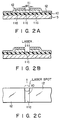
- a first embodiment of a trimming process by a laser beam according to the present invention will be described with reference to Figs. 2A through 2E.
- poly-silicone As shown in Fig. 2A, poly-silicone, approximately 5000 ⁇ thick, is deposited, by CVD process, over insulating (thermal silicon oxide) film 10, which has been layered on a semiconductor substrate, e.g., silicone substrate 5. Boron ions are implanted in the polysilicon, to form a shorting polysilicon layer of extremely small resistance, i.e., trimmed material 11.
- the insulating material may be any other suitable material other than silicon oxide, for example, PSG glass or silicone nitride.
- the insulating layer has preferably a thickness of 1.2 ⁇ or more, because its figure would prevents an adverse effect on silicone substrate 5 in the processings to be given later.
- shield metal film 12 which has higher reflectivity for laser beam than the polysilicon layer and a large heat conductivity, is applied over silicon substrate 5 and polysilicon layer 11. Then, the film is patterned to have an opening or a slit on a trimmed region 11c, through which polysilicon layer 11 is exposed. In this way, shield metal film (laser shield layer) 12 is formed.
- the step of forming shield metal film 12 may be preferably made at the same time of forming electrode wiring pattern. That is, the shield metal film 12 and the electrode wiring pattern for the resist film may be formed only one step of depositing metal and patterning the same.
- Shield metal film 12 is preferably made of any of aluminum, gold and platinum, or material essentially consisting of aluminum plus doped with impurity of silicone and/or copper.
- the thickness of shield metal film 12 is preferably 1 ⁇ or more, and when it is formed following the electrode forming step, it has preferably the same thickness as that of the electrode, e.g., abnout 4 ⁇ .
- a width W of trimmed region 11c is about 9 ⁇ m. As shown in Fig. 2B, trimmed region 11c was irradiated with a laser beam having a spot diameter of less than 9 ⁇ , and the trimmed material in this region was cut off through the vaporizing process.
- a laser trimming device used was LX84, which is commercially available and manufactured by LTX Co., Ltd.
- the trimming is made to separate trimmed material by scanning a laser beam in a direction as shown by an arrow.
- the diameter of laser spot is set to 10 ⁇
- the opening or slot of metal film 12 is set to be slightly narrow and to 9 ⁇ in this embodiment .
- the diameter of a laser spot should be larger than the width of the slot of shield metal 12.
- the slight difference between the spot diameter and the slot width may be preferabl, which are selected to a different length of 5 ⁇ 15%.
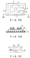
- Fig. 2D shows one example of an electric circuit using polysilicon layer 11 for short-circuiting. In this example, to obtain a resistance of resistor 14, polysilicone layer 11 is cut off (as indicated by mark X) by the trimming process according to present invention.
- a power distribution of the laser beam incident on the trimmed material 11 is as shown in Fig. 2E.
- the distribution curve of of the laser power absorbed by the trimmed material was plotted under the condition that the center A of the applied laser spot is set at the center of trimmed region 11c.
- the laser beam on the fringe of the trimmed portion is reflected by shield metal film 12 and does not reach the trimmed material thereunder. This indicates that only the trimmed material right under opening 13 of shield metal film 12 is evaporated by the laser beam.
- the untrimmed region of the trimmed material is of course heated by the heat laterally transferred from evaporation region 11c, but its temperature rise is small and its melting hardly progresses, because most of the heat from the evaporation region is absorbed by shield metal film 12 of good heat conductivity. Therefore, melting region 1b as shown in Fig. 1C is remarkably reduced, so that a phase of the trimmed material shifts from evaporation region 11c to solidus region 11a through the very narrow melting region.
- the melting region possibly causing the protruded portion is remarkably reduced.
- the shield metal film is layered just above the melting region, occurrence of the protrusion in the fringe of the trimmed region is minimized.
- resistor film 11 made of Ni-Cr alloy
- resistor film 11 is made of Ni-Cr alloy.
- An insulating layer, e.g., SiO2 film 25, is interlayered between resistor film 11 and shield metal film 12.
- the insulating layer, which is for electrically insulating the films 11 and 12 one from another, is formed by CVD process, for example, and is made of PSG or silicon nitride.
- trimmed material 11 is made of silicone, it may be a thermal silicon oxide film.
- a preferable thickness of insulating layer 25 is 1000 ⁇ or less. This figure allows shield metal film 12 to well absorb the the heat of the trimmed material.
- resistance film 11 is connected in parallel with resistor 24 of 2 ohms, for example, is used as a resistor element of 1 ohm. If necessary, it is disconnected or cut off (as indicated by mark X) from resistor 24 and is used as a resistor element of 2 ohms.
- the trimmed material 11 with insulating film 2 layered thereover is irradiated with the laser beam, the trimmed material could be vaporized through the insulating film.
- the insulating layer may be layered over the region to be irradiated with the laser beam, as shown in Fig. 4.
- shield metal film 12 may be provided on only one side of the laser irradiated region.
- the present invention is applicable for the trimmed material formed over an insulating substrate such as a ceramic substrate. If the shield metal film has a higher reflectivity for laser beam than the trimmed material or a good heat conductivity, is used, the beneficial effects by the present invention may sometimes be obtained. To reliably obtain such effects, it is preferable that the shield metal film is excellent in both the reflectivity and the heat conductivity.
- a trimming process by a laser beam according to the present invention, after the upper surface of the untrimmed region of a trimmed material is covered with a predetermined shield metal film, the trimming process based on the laser beam irradiation is performed.
- a resulting melting region of the trimmed material which will cause a protruded portion, is very narrow, thus minimizing formation of the protruded portion. Therefore, a protecting film formed over the structure thus formed is reliable and can hermetically protect the structure for a long time.
Landscapes
- Engineering & Computer Science (AREA)
- Physics & Mathematics (AREA)
- Optics & Photonics (AREA)
- Plasma & Fusion (AREA)
- Manufacturing & Machinery (AREA)
- Microelectronics & Electronic Packaging (AREA)
- Apparatuses And Processes For Manufacturing Resistors (AREA)
- Semiconductor Integrated Circuits (AREA)
- Design And Manufacture Of Integrated Circuits (AREA)
Applications Claiming Priority (2)
| Application Number | Priority Date | Filing Date | Title |
|---|---|---|---|
| JP63005566A JPH01184861A (ja) | 1988-01-13 | 1988-01-13 | レーザ光によるトリミング方法 |
| JP5566/88 | 1988-01-13 |
Publications (3)
| Publication Number | Publication Date |
|---|---|
| EP0324407A2 true EP0324407A2 (fr) | 1989-07-19 |
| EP0324407A3 EP0324407A3 (en) | 1990-10-17 |
| EP0324407B1 EP0324407B1 (fr) | 1994-10-26 |
Family
ID=11614760
Family Applications (1)
| Application Number | Title | Priority Date | Filing Date |
|---|---|---|---|
| EP89100264A Expired - Lifetime EP0324407B1 (fr) | 1988-01-13 | 1989-01-09 | Procédé d'ajustage par rayon laser |
Country Status (5)
| Country | Link |
|---|---|
| US (1) | US4928838A (fr) |
| EP (1) | EP0324407B1 (fr) |
| JP (1) | JPH01184861A (fr) |
| KR (1) | KR920004516B1 (fr) |
| DE (1) | DE68918955T2 (fr) |
Cited By (5)
| Publication number | Priority date | Publication date | Assignee | Title |
|---|---|---|---|---|
| EP0361439A3 (en) * | 1988-09-30 | 1990-08-16 | Kabushiki Kaisha Toshiba | Trimming resistor element for microelectronic circuit |
| EP1003217A3 (fr) * | 1998-11-06 | 2001-03-14 | Matsushita Electric Industrial Co., Ltd. | Réseau de résistances régulé, dispositif semi-conducteur comprenant ce réseau de résistance, et méthode de fabrication |
| DE10141352A1 (de) * | 2001-08-23 | 2003-06-05 | Osram Opto Semiconductors Gmbh | Verfahren zur Oberflächenbehandlung eines Halbleiters |
| EP1414280A3 (fr) * | 2002-10-16 | 2006-06-14 | Hitachi, Ltd. | Dispositif électronique multicouche et sa méthode d'obtention |
| WO2012099635A3 (fr) * | 2010-10-28 | 2012-12-27 | President And Fellows Of Harvard College | Traitement par faisceau d'électrons à l'aide de glace condensée |
Families Citing this family (13)
| Publication number | Priority date | Publication date | Assignee | Title |
|---|---|---|---|---|
| JP2584884B2 (ja) * | 1990-05-31 | 1997-02-26 | 株式会社日立製作所 | 配線基板 |
| US5068513A (en) * | 1990-09-28 | 1991-11-26 | Beloit Corporation | Water jet slitter with laser finish and method |
| US5213649A (en) * | 1990-10-15 | 1993-05-25 | Beloit Technologies, Inc. | Apparatus for receiving and cutting a continuous web |
| US5235154A (en) * | 1992-04-28 | 1993-08-10 | International Business Machines Corporation | Laser removal of metal interconnects |
| US5347423A (en) * | 1992-08-24 | 1994-09-13 | Murata Erie North America, Inc. | Trimmable composite multilayer capacitor and method |
| US5345361A (en) * | 1992-08-24 | 1994-09-06 | Murata Erie North America, Inc. | Shorted trimmable composite multilayer capacitor and method |
| KR100431179B1 (ko) * | 2001-12-04 | 2004-05-12 | 삼성전기주식회사 | 온도보상 수정발진기 및 그 출력주파수조정방법 |
| US20030129396A1 (en) * | 2001-12-27 | 2003-07-10 | Gerhard Kiessling | Coating composition for metal conductors and coating process involving the use thereof |
| KR100826633B1 (ko) * | 2002-03-28 | 2008-05-02 | 지에스아이 루모닉스 코포레이션 | 소자배열의 고속, 정밀한 마이크로머시닝을 위한 방법 및 시스템 |
| JP4137888B2 (ja) | 2003-05-13 | 2008-08-20 | 富士通株式会社 | 半導体集積回路装置 |
| US8426745B2 (en) * | 2009-11-30 | 2013-04-23 | Intersil Americas Inc. | Thin film resistor |
| JP5666411B2 (ja) * | 2011-09-30 | 2015-02-12 | セイコーインスツル株式会社 | 半導体装置 |
| CN112687558B (zh) * | 2020-12-05 | 2024-06-28 | 西安翔腾微电子科技有限公司 | 一种改善激光修调多晶硅电阻精度的方法 |
Family Cites Families (8)
| Publication number | Priority date | Publication date | Assignee | Title |
|---|---|---|---|---|
| US4146673A (en) * | 1977-10-27 | 1979-03-27 | E. I. Du Pont De Nemours And Company | Process of film resistor laser trimming and composition of removable coating used therein |
| US4272775A (en) * | 1978-07-03 | 1981-06-09 | National Semiconductor Corporation | Laser trim protection process and structure |
| US4179310A (en) * | 1978-07-03 | 1979-12-18 | National Semiconductor Corporation | Laser trim protection process |
| US4374314A (en) * | 1981-08-17 | 1983-02-15 | Analog Devices, Inc. | Laser template trimming of circuit elements |
| EP0164564A1 (fr) * | 1984-05-18 | 1985-12-18 | Siemens Aktiengesellschaft | Agencement pour la fabrication de trous borgnes dans une construction laminée |
| JPH0789567B2 (ja) * | 1985-02-25 | 1995-09-27 | 株式会社日立製作所 | 半導体装置 |
| JPH0640563B2 (ja) * | 1985-03-13 | 1994-05-25 | 株式会社東芝 | 膜抵抗体のレ−ザトリミング方法 |
| JPS6288338A (ja) * | 1985-10-15 | 1987-04-22 | Nec Corp | 半導体記憶装置 |
-
1988
- 1988-01-13 JP JP63005566A patent/JPH01184861A/ja active Pending
-
1989
- 1989-01-04 US US07/293,278 patent/US4928838A/en not_active Expired - Lifetime
- 1989-01-07 KR KR1019890000120A patent/KR920004516B1/ko not_active Expired
- 1989-01-09 DE DE68918955T patent/DE68918955T2/de not_active Expired - Fee Related
- 1989-01-09 EP EP89100264A patent/EP0324407B1/fr not_active Expired - Lifetime
Cited By (8)
| Publication number | Priority date | Publication date | Assignee | Title |
|---|---|---|---|---|
| EP0361439A3 (en) * | 1988-09-30 | 1990-08-16 | Kabushiki Kaisha Toshiba | Trimming resistor element for microelectronic circuit |
| US5065221A (en) * | 1988-09-30 | 1991-11-12 | Kabushiki Kaisha Toshiba | Trimming resistor element for microelectronic circuit |
| EP1003217A3 (fr) * | 1998-11-06 | 2001-03-14 | Matsushita Electric Industrial Co., Ltd. | Réseau de résistances régulé, dispositif semi-conducteur comprenant ce réseau de résistance, et méthode de fabrication |
| US6649463B2 (en) | 1998-11-06 | 2003-11-18 | Matsushita Electric Industrial Co., Ltd. | Regulating resistor network, semiconductor device including the resistor network, and method for fabricating the device |
| DE10141352A1 (de) * | 2001-08-23 | 2003-06-05 | Osram Opto Semiconductors Gmbh | Verfahren zur Oberflächenbehandlung eines Halbleiters |
| EP1414280A3 (fr) * | 2002-10-16 | 2006-06-14 | Hitachi, Ltd. | Dispositif électronique multicouche et sa méthode d'obtention |
| US7105911B2 (en) | 2002-10-16 | 2006-09-12 | Hitachi, Ltd. | Multilayer electronic substrate, and the method of manufacturing multilayer electronic substrate |
| WO2012099635A3 (fr) * | 2010-10-28 | 2012-12-27 | President And Fellows Of Harvard College | Traitement par faisceau d'électrons à l'aide de glace condensée |
Also Published As
| Publication number | Publication date |
|---|---|
| US4928838A (en) | 1990-05-29 |
| KR920004516B1 (ko) | 1992-06-08 |
| KR890012365A (ko) | 1989-08-26 |
| JPH01184861A (ja) | 1989-07-24 |
| DE68918955D1 (de) | 1994-12-01 |
| EP0324407A3 (en) | 1990-10-17 |
| EP0324407B1 (fr) | 1994-10-26 |
| DE68918955T2 (de) | 1995-02-23 |
Similar Documents
| Publication | Publication Date | Title |
|---|---|---|
| EP0324407B1 (fr) | Procédé d'ajustage par rayon laser | |
| US4751197A (en) | Make-link programming of semiconductor devices using laser enhanced thermal breakdown of insulator | |
| US5329152A (en) | Ablative etch resistant coating for laser personalization of integrated circuits | |
| US4912066A (en) | Make-link programming of semiconductor devices using laser-enhanced thermal breakdown of insulator | |
| US5065221A (en) | Trimming resistor element for microelectronic circuit | |
| US4617723A (en) | Method and device for creating an activatable conducting link in a semiconductor device | |
| US5087589A (en) | Selectively programmable interconnections in multilayer integrated circuits | |
| EP0075926A2 (fr) | Dispositif semiconducteur à circuit intégré | |
| US4835118A (en) | Non-destructive energy beam activated conductive links | |
| KR920003467B1 (ko) | 트리밍소자와 그 전기단락방법 | |
| JP2001068629A (ja) | バリア屈折層または非反射層を用いた薄膜抵抗のレーザトリム特性の改良 | |
| US4968643A (en) | Method for fabricating an activatable conducting link for metallic conductive wiring in a semiconductor device | |
| US7804391B2 (en) | Changing an electrical resistance of a resistor | |
| EP0539197A1 (fr) | Dispositif semi-conducteur comprenant un anti-fusible et procédé de fabrication | |
| EP0189598B1 (fr) | Procédé de fabrication d'un dispositif semi-conducteur | |
| US5675174A (en) | Method for using fuse structure in semiconductor device | |
| US5266529A (en) | Focused ion beam for thin film resistor trim on aluminum nitride substrates | |
| EP0272799A1 (fr) | Couche destructurable et résistant à la gravure pour la personnalisation par laser de circuits intégrés | |
| USH546H (en) | Formation of thin-film resistors on silicon substrates | |
| US6764953B2 (en) | Electronic device, and method of patterning a first layer | |
| KR950001758B1 (ko) | 반도체 장치 | |
| JPH0760853B2 (ja) | レ−ザ・ビ−ムでプログラムし得る半導体装置と半導体装置の製法 | |
| EP0263574A1 (fr) | Méthode pour fabriquer un dispositif semi-conducteur et un tel dispositif ayant au moins une ligne conductrice activable sélectivement | |
| JP2508293B2 (ja) | 半導体装置及びその製造方法 | |
| EP0258962A2 (fr) | Dispositifs semi-conducteurs à liens sélectifs et un procédé pour leur fabrication |
Legal Events
| Date | Code | Title | Description |
|---|---|---|---|
| PUAI | Public reference made under article 153(3) epc to a published international application that has entered the european phase |
Free format text: ORIGINAL CODE: 0009012 |
|
| 17P | Request for examination filed |
Effective date: 19890206 |
|
| AK | Designated contracting states |
Kind code of ref document: A2 Designated state(s): DE FR GB |
|
| PUAL | Search report despatched |
Free format text: ORIGINAL CODE: 0009013 |
|
| AK | Designated contracting states |
Kind code of ref document: A3 Designated state(s): DE FR GB |
|
| 17Q | First examination report despatched |
Effective date: 19921204 |
|
| GRAA | (expected) grant |
Free format text: ORIGINAL CODE: 0009210 |
|
| AK | Designated contracting states |
Kind code of ref document: B1 Designated state(s): DE FR GB |
|
| REF | Corresponds to: |
Ref document number: 68918955 Country of ref document: DE Date of ref document: 19941201 |
|
| ET | Fr: translation filed | ||
| PLBE | No opposition filed within time limit |
Free format text: ORIGINAL CODE: 0009261 |
|
| STAA | Information on the status of an ep patent application or granted ep patent |
Free format text: STATUS: NO OPPOSITION FILED WITHIN TIME LIMIT |
|
| 26N | No opposition filed | ||
| PGFP | Annual fee paid to national office [announced via postgrant information from national office to epo] |
Ref country code: GB Payment date: 19971231 Year of fee payment: 10 |
|
| PGFP | Annual fee paid to national office [announced via postgrant information from national office to epo] |
Ref country code: FR Payment date: 19980109 Year of fee payment: 10 |
|
| PG25 | Lapsed in a contracting state [announced via postgrant information from national office to epo] |
Ref country code: GB Free format text: LAPSE BECAUSE OF NON-PAYMENT OF DUE FEES Effective date: 19990109 |
|
| GBPC | Gb: european patent ceased through non-payment of renewal fee |
Effective date: 19990109 |
|
| PG25 | Lapsed in a contracting state [announced via postgrant information from national office to epo] |
Ref country code: FR Free format text: LAPSE BECAUSE OF NON-PAYMENT OF DUE FEES Effective date: 19990930 |
|
| REG | Reference to a national code |
Ref country code: FR Ref legal event code: ST |
|
| PGFP | Annual fee paid to national office [announced via postgrant information from national office to epo] |
Ref country code: DE Payment date: 20070104 Year of fee payment: 19 |
|
| PG25 | Lapsed in a contracting state [announced via postgrant information from national office to epo] |
Ref country code: DE Free format text: LAPSE BECAUSE OF NON-PAYMENT OF DUE FEES Effective date: 20080801 |