EP0324929B1 - Halbleiteranordnung mit Druckkontakten - Google Patents
Halbleiteranordnung mit Druckkontakten Download PDFInfo
- Publication number
- EP0324929B1 EP0324929B1 EP19880119894 EP88119894A EP0324929B1 EP 0324929 B1 EP0324929 B1 EP 0324929B1 EP 19880119894 EP19880119894 EP 19880119894 EP 88119894 A EP88119894 A EP 88119894A EP 0324929 B1 EP0324929 B1 EP 0324929B1
- Authority
- EP
- European Patent Office
- Prior art keywords
- electrode
- insulator
- external
- external electrode
- temperature compensator
- Prior art date
- Legal status (The legal status is an assumption and is not a legal conclusion. Google has not performed a legal analysis and makes no representation as to the accuracy of the status listed.)
- Expired - Lifetime
Links
Images


Classifications
-
- H—ELECTRICITY
- H10—SEMICONDUCTOR DEVICES; ELECTRIC SOLID-STATE DEVICES NOT OTHERWISE PROVIDED FOR
- H10W—GENERIC PACKAGES, INTERCONNECTIONS, CONNECTORS OR OTHER CONSTRUCTIONAL DETAILS OF DEVICES COVERED BY CLASS H10
- H10W72/00—Interconnections or connectors in packages
-
- H—ELECTRICITY
- H10—SEMICONDUCTOR DEVICES; ELECTRIC SOLID-STATE DEVICES NOT OTHERWISE PROVIDED FOR
- H10W—GENERIC PACKAGES, INTERCONNECTIONS, CONNECTORS OR OTHER CONSTRUCTIONAL DETAILS OF DEVICES COVERED BY CLASS H10
- H10W76/00—Containers; Fillings or auxiliary members therefor; Seals
- H10W76/10—Containers or parts thereof
- H10W76/12—Containers or parts thereof characterised by their shape
- H10W76/13—Containers comprising a conductive base serving as an interconnection
- H10W76/138—Containers comprising a conductive base serving as an interconnection having another interconnection being formed by a cover plate parallel to the conductive base, e.g. sandwich type
Definitions
- the present invention relates to a semiconductor device, and more particularly, it relates to a pressure-connection type semiconductor device such as a thyristor or a high-power transistor.
- Japanese Patent Laying-Open Gazette No. 79669/1987 discloses a conventional semiconductor device of this type.
- the cathode contacts with a metal electrode plate, which in turn contacts the semiconductor element.
- the contact areas of the cathode are made smaller than the corresponding areas of the metal electrode plates. This structure avoids deformation of the cathode, even when the metal electrode plates are not properly centered.
- the European patent application EP-A-0 220 698 discloses a GTO thyristor comprising island-shaped emitter zones.
- the surface not covered with emitter zones serves as the basis region and is covered with a gate electrode.
- the gate electrode is located at a central position of the semiconductor body and contacts same through a metal contact disc.
- This contact disc is located in a cavity or bore of the cathode electrode.
- the contact disc is insulated by an insulation sleeve and is urged to the semiconductor element by a spring.
- Fig. 1 is a sectional view showing another semiconductor device according to the prior art, similar to that of JP-A-62 079 669.
- a thyristor element 1 is provided in the form of a disc, wherein a gate electrode 1b and a cathode electrode 1c are provided on the lower surface of a semiconductor substrate 1a in inner and outer peripheral regions, respectively.
- An anode electrode 1d is provided on the upper surface of the semiconductor substrate 1a.
- a doughnut-shaped temperature compensator 2 is pressed against the cathode electrode 1c to get electrically in contact only with that.
- An external cathode electrode 3 is pressed against the temperature compensator 2 to get electrically in contact only with that.
- a discoidal external anode electrode 4 is pressed against the anode electrode 1d to get electrically in contact only with that.
- a flange 5a is provided on the outer peripheral region of the external cathode electrode 3, while a flange 5b is provided on the outer peripheral region of the external anode electrode 4.
- An insulating sleeve 6 couples these flanges 5a and 5b with each other, to thereby integrally couple the external cathode electrode 3 with the external anode electrode 4 while maintaining an electrically insulated state.
- a disc spring 7 and an insulator 8, the configuration of which is shown in Fig. 2, are received in this order in a cavity 3a defined in a central portion of the external cathode electrode 3.
- a gate lead 10 is inserted in a through hole 8a defined in an upper central portion of the insulator 8 and an insulating tube 9. The first end of the gate lead 10 is pressed against the gate electrode 1b to provide electrical contact by the spring force of the disc spring 7 through the insulator 8, while the second end thereof is electrically connected with a gate terminal 11.
- the assembly sequence of the semiconductor device shown in Fig. 1 is as follows: First, the gate lead 10 is inserted into the through hole 8a of the insulator 8 and the insulating tube 9, to thereby form an assembly A . Then the disc spring 7 and the assembly A are introduced in this order into the cavity 3a of the external cathode electrode 3, and the temperature compensator 2 is placed on the upper surface of the external cathode electrode 3. Further, the thyristor element 1 is so arranged that the temperature compensator 2 faces the cathode electrode 1c and that an end of the gate lead 10 faces the gate electrode 1b.
- the external anode electrode 4 is placed on the anode electrode 1d of the thyristor element 1, and the flanges 5a and 5b are coupled with each other by the insulating sleeve 6 while externally applying pressure to the external cathode electrode 3 and the external anode electrode 4.
- Fig. 3 illustrates the positional relation between the temperature compensator 2, the external cathode electrode 3, the insulator 8 and the gate lead 10.
- a clearance is defined between the insulator 8 and the gate lead 10 since the bore diameter a of the through hole 8a of the insulator 8 is larger than the outer diameter b of the gate lead 10, whereby misalignment may be caused between the insulator 8 and the gate lead 10.
- another clearance is defined between the insulator 8 and the external cathode electrode 3 since the inner diameter c of the cavity 3a of the external cathode electrode 3 is larger than the outer diameter d of the insulator 8, whereby misalignment may be caused between the external cathode electrode 3 and the insulator 8.
- a semiconductor device is provided according to the present invention as defined in Claim 1.
- a principal object of the present invention is to provide a semiconductor device which can correctly and easily perform alignment between the first electrode of the semiconductor element and the temperature compensator and between the second electrode of the semiconductor element and the second external electrode.
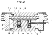
- Fig. 5 is a sectional view showing a semiconductor device according to an embodiment of the present invention.
- the thyristor element 1 is similar in structure to that of the prior art shown in Fig. 1.
- the through hole 2a is defined in a central portion of a temperature compensator 2 and the cavity 3a is defined in an upper central portion of the external cathode electrode 3, respectively.
- the inner diameter of the through hole 2a is preferably smaller than that of the cavity 3a, while the former may be identical to the latter.
- the upper surface of the external cathode electrode 3 faces the lower surface of the temperature compensator 2, while the external cathode electrode 3 is pressed against the temperature compensator 2 to be electrically in contact only with that.
- a space region defined by the through hole 2a and the cavity 3a is adapted to receive a disc spring 7, an insulating plate 12 and a substantially cylindrical insulator 13, being C-shaped in section and having an outer diameter equal to the inner diameter of the space region, in this order.
- the outer side surface of the insulator 13 is brought into close contact with the inner side surfaces of the through hole 2a and the cavity 3a.
- an elastic insulator having an outer diameter larger than the inner diameter of the space region may be employed so as to be fitted with pressure in the space region.
- the outer side surface of such an insulator is further strongly adhered to the inner side surfaces of the through hole 2a and the cavity 3a.
- An assembly B (Fig. 6B), which is assembled along the procedure shown in Fig. 6A, is fitted with pressure into the insulator 13.
- the bottom surface of an external gate electrode 14 forming the assembly B is upwardly urged by spring force of the disc spring 7 through the insulating plate 12, so that the upper surface thereof is pressed against the gate electrode 1b to get electrically in contact with that.
- the temperature compensator 2 which is doughnut-shaped similarly to that of the prior art, is pressed against the cathode electrode 1c to get electrically in contact only with that.
- the discoidal external anode electrode 4 is pressed against the anode electrode 1d to get electrically in contact with that.
- the flange 5a is provided on the outer periphery of the external cathode electrode 3, while the other flange 5b is provided on the outer periphery of the external anode electrode 4.
- flanges 5a and 5b are coupled with each other by the insulating sleeve 6 while externally applying pressure onto the external cathode electrode 3 and the external anode electrode 4, to thereby integrally couple the external cathode electrode 3 with the external anode electrode 4, whereas there is an electrically insulated state between the external cathode electrode 3 and the external anode electrode 4.
- the substantially cylindrical insulator 13 being C-shaped in section and having an outer diameter equal to or larger than the inner diameter of the space region defined by the through hole 2a of the temperature compensator 2 and the cavity 3a of the external cathode electrode 3, is fitted with pressure into the space region in this embodiment, whereby the insulator 13 is adhered to the external cathode electrode 3 as well as to the temperature compensator 2.
- the assembly B (Fig. 6B) is fitted with pressure into the insulator 13, whereby the insulator 13 is adhered to the external gate electrode 14 forming the assembly B .
- the insulator 13 locates the external gate electrode 14 in prescribed positional relation to the temperature compensator 2 and the external cathode electrode 3.
- Fig. 7 is a sectional view illustrating the semiconductor device shown in Fig. 5 in a state before assembling.
- the semiconductor device shown in Fig. 5 is assembled in the following manner:
- an O-ring 15 is mounted in an annular groove 14a of the external gate electrode 14 and a gate lead 16 is inserted into the insulating tube 9 as shown in Fig. 6A, to thereby form the assembly B shown in Fig. 6B.
- the inner diameter of the O-ring 15 is preferably set to be smaller than the outer diameter of the external gate electrode 14 in the portion of the annular groove 14a. Further, it is necessary to set the outer diameter of the O-ring 15 to be larger than the inner diameter of the insulator 13 upon completion of the assembly B .
- the insulating sleeve 6, the external cathode electrode 3, the flanges 5a and 5c and a gate pipe 17 are respectively brazed by silver solder (not shown) or the like, to thereby form an assembly C .
- the external anode electrode 4 and the flange 5b are brazed by silver solder (not shown) or the like, to thereby form an assembly D .
- the disc spring 7, the insulating plate 12 and the insulator 13 are introduced in this order into the cavity 3a which is defined in the central portion of the external cathode electrode 3.
- a part (external gate electrode 14) of the assembly B is fitted with pressure in the insulator 13, while a part of the gate lead 16 not covered with the insulating tube 9 is inserted into the gate pipe 17.
- the insulator 13 is engaged into the through hole 2a of the temperature compensator 2, while a lower surface 2b of the temperature compensator 2 is placed on an upper surface 3b of the external cathode electrode 3.
- the thyristor element 1 and the assembly D are arranged in this order on the temperature compensator 2, then the outer peripheries of the flanges 5b and 5c are arcwelded with external applying pressure to the external cathode electrode 3 and the external anode electrode 4.
- the semiconductor device is so assembled that the thyristor element 1, the temperature compensator 2, the external cathode electrode 3, the external gate electrode 14 and the external anode electrode 4 are pressure-connected with each other.
- the O-ring 15 is employed in order to improve adhesion between the insulator 13 and the external gate electrode 14.
- the semiconductor element is implemented by the thyristor element 1 in the above embodiment, such a semiconductor element may be prepared by a static induction thyristor, a gate turn-off thyristor or a high-power transistor.
- the present invention can be applied to the static induction type thyristor et al., wherein a gate electrode and a cathode electrode (or source or emitter electrode) can be easily and correctly aligned with an external gate electrode and a temperature compensator, respectively.
Landscapes
- Thyristors (AREA)
- Die Bonding (AREA)
Claims (3)
- Halbleitervorrichtung, die folgendes aufweist:- ein Halbleiterelement (1) mit einer ersten Elektrode (1c) und einer zweiten Elektrode (1b), die in einem ersten bzw. zweiten Bereich einer ersten Oberfläche vorgesehen sind;- eine erste externe Elektrode (3) mit einem Hohlraum (3a) in einem Bereich, der der zweiten Elektrode (1b) zugewandt gegenüberliegt;- eine Temperaturausgleichseinrichtung (2), die in einem der zweiten Elektrode (1b) gegenüberliegenden Bereich mit einem Durchgangsloch (2a) versehen ist und die eine Oberfläche aufweist, die für den Kontakt mit der Oberfläche der ersten Elektrode (1c) angeordnet ist, wobei die eine Oberfläche (3b) der ersten externen Elektrode (3) für den Kontakt mit einer anderen Oberfläche (2b) der Temperaturausgleichseinrichtung (2) angeordnet ist;- eine zweite externe Elektrode (14), die in einem Raum, der durch Ausfluchten des Hohlraums (3a) und des Durchgangslochs (2a) der Temperaturausgleichseinrichtung gebildet ist, angeordnet ist und mit einer Oberfläche der zweiten Elektrode (1b) in Kontakt steht;- einen Isolator (13), der sich an der Innenseite des Hohlraums (3a) befindet und als zylindrisches Element ausgebildet ist, das zwischen der Außenseite der zweiten externen Elektrode (14) und der Innenseite des Hohlraums (3a) angeordnet ist, und- Druckverbindungseinrichtungen (5a, 5b, 7) zum Aufbringen von Druck auf das Halbleiterelement (1) und die erste externe Elektrode (3), um eine Druckverbindung zwischen der ersten Elektrode (1c) und der zweiten Elektrode (1b) mit dem Halbleiterelement (1) herzustellen und einen Druck zwischen der zweiten Elektrode (1b) und der zweiten externen Elektrode (14) aufzubringen,dadurch gekennzeichnet,- daß das Durchgangsloch (2a) der Temperaturausgleichseinrichtung (2) und der Hohlraum (3a) der ersten externen Elektrode (3) gleichen Innendurchmesser aufweisen;- daß der zylindrische Isolator (13) als elastisches Element mit C-förmigem Querschnitt ausgebildet ist und ebenfalls zwischen der Außenseite der zweiten externen Elektrode (14) und der Innenseite des Durchgangslochs (2a) angeordnet ist;- wobei der Außendurchmesser des Isolators (13) im demontierten Zustand größer ist als der Innendurchmesser des Raumbereichs, so daß der Isolator (13) im montierten Zustand im Preßsitz in den Raumbereich eingepaßt ist;- daß die zweite externe Elektrode (14) mit einer ringförmigen Nut (14a) versehen ist, in der ein im Schnappsitz eingepaßter O-Ring (15) positioniert ist, wobei der O-Ring (15) zwischen der äußeren Seitenfläche der zweiten externen Elektrode (14) und der inneren Seitenfläche des Isolators (13) angeordnet ist;- wobei die Druckverbindungseinrichtungen (5a, 5b, 7) Druckkontakt-Übergangsflächen zwischen der ersten Elektrode (1c) und der Temperaturausgleichseinrichtung (2) schaffen.
- Vorrichtung nach Anspruch 1,
wobei die zweite externe Elektrode (14) eine zylindrische Gestalt aufweist und an ihrem einen Ende in Richtung zu der zweiten Elektrode (1b) abgeschrägt ist. - Vorrichtung nach Anspruch 1 oder 2,
wobei die zweite externe Elektrode (14) mit der Außenseite mittels einer Leitung (16) verbunden ist, die in ein Isolierrohr (9) eingeführt ist.
Applications Claiming Priority (2)
| Application Number | Priority Date | Filing Date | Title |
|---|---|---|---|
| JP308055/87 | 1987-12-03 | ||
| JP62308055A JPH0831488B2 (ja) | 1987-12-03 | 1987-12-03 | 半導体装置 |
Publications (3)
| Publication Number | Publication Date |
|---|---|
| EP0324929A2 EP0324929A2 (de) | 1989-07-26 |
| EP0324929A3 EP0324929A3 (de) | 1990-01-10 |
| EP0324929B1 true EP0324929B1 (de) | 1997-11-05 |
Family
ID=17976341
Family Applications (1)
| Application Number | Title | Priority Date | Filing Date |
|---|---|---|---|
| EP19880119894 Expired - Lifetime EP0324929B1 (de) | 1987-12-03 | 1988-11-29 | Halbleiteranordnung mit Druckkontakten |
Country Status (4)
| Country | Link |
|---|---|
| US (1) | US5047836A (de) |
| EP (1) | EP0324929B1 (de) |
| JP (1) | JPH0831488B2 (de) |
| DE (1) | DE3856061T2 (de) |
Families Citing this family (6)
| Publication number | Priority date | Publication date | Assignee | Title |
|---|---|---|---|---|
| JP3153638B2 (ja) * | 1992-06-26 | 2001-04-09 | 三菱電機株式会社 | 圧接型半導体装置及びその製造方法並びに熱補償板 |
| JP3471880B2 (ja) * | 1994-02-23 | 2003-12-02 | 三菱電機株式会社 | 圧接型半導体装置 |
| DE10041112B4 (de) * | 2000-08-22 | 2006-05-24 | eupec Europäische Gesellschaft für Leistungshalbleiter mbH & Co. KG | Isolierelement |
| DE102005055713B4 (de) * | 2005-11-23 | 2011-11-17 | Semikron Elektronik Gmbh & Co. Kg | Leistungshalbleitermodul mit Anschlusselementen |
| EP2071621A1 (de) | 2007-12-11 | 2009-06-17 | ABB Research Ltd. | Halbleiterschaltungsanordnung mit Gate-Anschluß |
| CN109494206B (zh) * | 2017-09-12 | 2022-05-24 | 株洲中车时代半导体有限公司 | 一种晶闸管 |
Family Cites Families (10)
| Publication number | Priority date | Publication date | Assignee | Title |
|---|---|---|---|---|
| DE2103146A1 (de) * | 1970-01-26 | 1971-08-05 | Westinghouse Electric Corp | Mittels einer Gate Elektrode Steuer bares Schaltelement |
| JPS5147577B2 (de) * | 1973-06-12 | 1976-12-15 | ||
| DE2641483A1 (de) * | 1976-09-15 | 1978-03-16 | Siemens Ag | Halbleiterbauelement |
| JPS57104283U (de) * | 1980-12-17 | 1982-06-26 | ||
| JPS58207644A (ja) * | 1982-05-29 | 1983-12-03 | Toshiba Corp | 半導体装置 |
| JPS6063945U (ja) * | 1983-10-05 | 1985-05-07 | 日本インター株式会社 | 加圧接触型半導体装置 |
| JPH065685B2 (ja) * | 1984-06-20 | 1994-01-19 | 株式会社日立製作所 | 加圧接触形半導体装置 |
| JPS61136269A (ja) * | 1984-12-07 | 1986-06-24 | Hitachi Ltd | 半導体装置 |
| JPS62101072A (ja) * | 1985-10-25 | 1987-05-11 | シ−メンス、アクチエンゲゼルシヤフト | サイリスタ |
| JPH0770552B2 (ja) * | 1986-03-29 | 1995-07-31 | 三菱電機株式会社 | 半導体装置 |
-
1987
- 1987-12-03 JP JP62308055A patent/JPH0831488B2/ja not_active Expired - Lifetime
-
1988
- 1988-11-29 DE DE3856061T patent/DE3856061T2/de not_active Expired - Fee Related
- 1988-11-29 EP EP19880119894 patent/EP0324929B1/de not_active Expired - Lifetime
-
1990
- 1990-10-02 US US07/593,383 patent/US5047836A/en not_active Expired - Fee Related
Non-Patent Citations (1)
| Title |
|---|
| Patent Abstracts of Japan, vol. 11, no. 280 (E-539)[2727];& JP-A-62 079 669 * |
Also Published As
| Publication number | Publication date |
|---|---|
| JPH0831488B2 (ja) | 1996-03-27 |
| DE3856061D1 (de) | 1997-12-11 |
| EP0324929A3 (de) | 1990-01-10 |
| JPH01147837A (ja) | 1989-06-09 |
| US5047836A (en) | 1991-09-10 |
| EP0324929A2 (de) | 1989-07-26 |
| DE3856061T2 (de) | 1998-06-10 |
Similar Documents
| Publication | Publication Date | Title |
|---|---|---|
| US5278434A (en) | Pressure engagement structure for a full press-pack type semiconductor device | |
| US3299328A (en) | Semiconductor device with pressure contact | |
| US4587550A (en) | Press-packed semiconductor device with lateral fixing member | |
| EP1009067B1 (de) | Steckeranordnung | |
| EP0324929B1 (de) | Halbleiteranordnung mit Druckkontakten | |
| EP0158749A1 (de) | Halbleiteranordnung mit unter Druck stehenden Gliedern | |
| EP0477801B1 (de) | Optische Halbleiter-Vorrichtung | |
| EP0432796B1 (de) | Halbleiteranordnung | |
| JPH07221286A (ja) | 加圧組立半導体装置のためのゲート結合システム | |
| JPH033971Y2 (de) | ||
| JPS6127901B2 (de) | ||
| JPH06252280A (ja) | 平形半導体装置 | |
| US3196325A (en) | Electrode connection to mesa type semiconductor device | |
| US3553538A (en) | Pressure contact semiconductor device | |
| JPS6116687Y2 (de) | ||
| JPH02220452A (ja) | 半導体装置 | |
| JP2571916Y2 (ja) | 圧接型半導体素子 | |
| JPS6041459B2 (ja) | 半導体装置 | |
| JPH01293543A (ja) | 半導体装置 | |
| JPS61156768A (ja) | 半導体装置 | |
| GB2162366A (en) | Semiconductor device contact arrangements | |
| JP3005331B2 (ja) | 半導体装置 | |
| JPS6432682A (en) | Optoelectronic semiconductor | |
| JPH0777469A (ja) | 半導体圧力検出装置 | |
| JP2598573B2 (ja) | 圧接型半導体装置 |
Legal Events
| Date | Code | Title | Description |
|---|---|---|---|
| PUAI | Public reference made under article 153(3) epc to a published international application that has entered the european phase |
Free format text: ORIGINAL CODE: 0009012 |
|
| AK | Designated contracting states |
Kind code of ref document: A2 Designated state(s): DE FR GB IT |
|
| PUAL | Search report despatched |
Free format text: ORIGINAL CODE: 0009013 |
|
| RHK1 | Main classification (correction) |
Ipc: H01L 23/34 |
|
| AK | Designated contracting states |
Kind code of ref document: A3 Designated state(s): DE FR GB IT |
|
| 17P | Request for examination filed |
Effective date: 19900221 |
|
| 17Q | First examination report despatched |
Effective date: 19920610 |
|
| GRAG | Despatch of communication of intention to grant |
Free format text: ORIGINAL CODE: EPIDOS AGRA |
|
| GRAH | Despatch of communication of intention to grant a patent |
Free format text: ORIGINAL CODE: EPIDOS IGRA |
|
| GRAH | Despatch of communication of intention to grant a patent |
Free format text: ORIGINAL CODE: EPIDOS IGRA |
|
| GRAA | (expected) grant |
Free format text: ORIGINAL CODE: 0009210 |
|
| AK | Designated contracting states |
Kind code of ref document: B1 Designated state(s): DE FR GB IT |
|
| ITF | It: translation for a ep patent filed | ||
| REF | Corresponds to: |
Ref document number: 3856061 Country of ref document: DE Date of ref document: 19971211 |
|
| ET | Fr: translation filed | ||
| REG | Reference to a national code |
Ref country code: GB Ref legal event code: 727A |
|
| REG | Reference to a national code |
Ref country code: GB Ref legal event code: 727 |
|
| PLBE | No opposition filed within time limit |
Free format text: ORIGINAL CODE: 0009261 |
|
| STAA | Information on the status of an ep patent application or granted ep patent |
Free format text: STATUS: NO OPPOSITION FILED WITHIN TIME LIMIT |
|
| REG | Reference to a national code |
Ref country code: GB Ref legal event code: 727B |
|
| REG | Reference to a national code |
Ref country code: GB Ref legal event code: SP |
|
| 26N | No opposition filed | ||
| PGFP | Annual fee paid to national office [announced via postgrant information from national office to epo] |
Ref country code: FR Payment date: 19981110 Year of fee payment: 11 |
|
| PGFP | Annual fee paid to national office [announced via postgrant information from national office to epo] |
Ref country code: GB Payment date: 19981204 Year of fee payment: 11 |
|
| PGFP | Annual fee paid to national office [announced via postgrant information from national office to epo] |
Ref country code: DE Payment date: 19981207 Year of fee payment: 11 |
|
| ITPR | It: changes in ownership of a european patent |
Owner name: OFFERTA DI LICENZA AL PUBBLICO;AL PUBBLICO |
|
| REG | Reference to a national code |
Ref country code: GB Ref legal event code: 746 Effective date: 19990519 |
|
| REG | Reference to a national code |
Ref country code: FR Ref legal event code: D6 |
|
| PG25 | Lapsed in a contracting state [announced via postgrant information from national office to epo] |
Ref country code: GB Free format text: LAPSE BECAUSE OF NON-PAYMENT OF DUE FEES Effective date: 19991129 |
|
| GBPC | Gb: european patent ceased through non-payment of renewal fee |
Effective date: 19991129 |
|
| PG25 | Lapsed in a contracting state [announced via postgrant information from national office to epo] |
Ref country code: FR Free format text: LAPSE BECAUSE OF NON-PAYMENT OF DUE FEES Effective date: 20000731 |
|
| PG25 | Lapsed in a contracting state [announced via postgrant information from national office to epo] |
Ref country code: DE Free format text: LAPSE BECAUSE OF NON-PAYMENT OF DUE FEES Effective date: 20000901 |
|
| REG | Reference to a national code |
Ref country code: FR Ref legal event code: ST |
|
| PG25 | Lapsed in a contracting state [announced via postgrant information from national office to epo] |
Ref country code: IT Free format text: LAPSE BECAUSE OF NON-PAYMENT OF DUE FEES;WARNING: LAPSES OF ITALIAN PATENTS WITH EFFECTIVE DATE BEFORE 2007 MAY HAVE OCCURRED AT ANY TIME BEFORE 2007. THE CORRECT EFFECTIVE DATE MAY BE DIFFERENT FROM THE ONE RECORDED. Effective date: 20051129 |