EP0325342B1 - Verfahren zum Herstellen eines komplementären BICMOS-Transistors mit isoliertem vertikalem PNP-Transistor - Google Patents
Verfahren zum Herstellen eines komplementären BICMOS-Transistors mit isoliertem vertikalem PNP-Transistor Download PDFInfo
- Publication number
- EP0325342B1 EP0325342B1 EP89300019A EP89300019A EP0325342B1 EP 0325342 B1 EP0325342 B1 EP 0325342B1 EP 89300019 A EP89300019 A EP 89300019A EP 89300019 A EP89300019 A EP 89300019A EP 0325342 B1 EP0325342 B1 EP 0325342B1
- Authority
- EP
- European Patent Office
- Prior art keywords
- collector
- base
- implant
- pnp transistor
- transistor
- Prior art date
- Legal status (The legal status is an assumption and is not a legal conclusion. Google has not performed a legal analysis and makes no representation as to the accuracy of the status listed.)
- Expired - Lifetime
Links
Images



Classifications
-
- H—ELECTRICITY
- H10—SEMICONDUCTOR DEVICES; ELECTRIC SOLID-STATE DEVICES NOT OTHERWISE PROVIDED FOR
- H10D—INORGANIC ELECTRIC SEMICONDUCTOR DEVICES
- H10D84/00—Integrated devices formed in or on semiconductor substrates that comprise only semiconducting layers, e.g. on Si wafers or on GaAs-on-Si wafers
- H10D84/01—Manufacture or treatment
- H10D84/0107—Integrating at least one component covered by H10D12/00 or H10D30/00 with at least one component covered by H10D8/00, H10D10/00 or H10D18/00, e.g. integrating IGFETs with BJTs
- H10D84/0109—Integrating at least one component covered by H10D12/00 or H10D30/00 with at least one component covered by H10D8/00, H10D10/00 or H10D18/00, e.g. integrating IGFETs with BJTs the at least one component covered by H10D12/00 or H10D30/00 being a MOS device
-
- H—ELECTRICITY
- H10—SEMICONDUCTOR DEVICES; ELECTRIC SOLID-STATE DEVICES NOT OTHERWISE PROVIDED FOR
- H10P—GENERIC PROCESSES OR APPARATUS FOR THE MANUFACTURE OR TREATMENT OF DEVICES COVERED BY CLASS H10
- H10P30/00—Ion implantation into wafers, substrates or parts of devices
- H10P30/20—Ion implantation into wafers, substrates or parts of devices into semiconductor materials, e.g. for doping
- H10P30/21—Ion implantation into wafers, substrates or parts of devices into semiconductor materials, e.g. for doping of electrically active species
-
- H—ELECTRICITY
- H10—SEMICONDUCTOR DEVICES; ELECTRIC SOLID-STATE DEVICES NOT OTHERWISE PROVIDED FOR
- H10D—INORGANIC ELECTRIC SEMICONDUCTOR DEVICES
- H10D84/00—Integrated devices formed in or on semiconductor substrates that comprise only semiconducting layers, e.g. on Si wafers or on GaAs-on-Si wafers
- H10D84/01—Manufacture or treatment
- H10D84/0112—Integrating together multiple components covered by H10D8/00, H10D10/00 or H10D18/00, e.g. integrating multiple BJTs
- H10D84/0119—Integrating together multiple components covered by H10D8/00, H10D10/00 or H10D18/00, e.g. integrating multiple BJTs the components including complementary BJTs
- H10D84/0121—Integrating together multiple components covered by H10D8/00, H10D10/00 or H10D18/00, e.g. integrating multiple BJTs the components including complementary BJTs the complementary BJTs being vertical BJTs
-
- H—ELECTRICITY
- H10—SEMICONDUCTOR DEVICES; ELECTRIC SOLID-STATE DEVICES NOT OTHERWISE PROVIDED FOR
- H10D—INORGANIC ELECTRIC SEMICONDUCTOR DEVICES
- H10D84/00—Integrated devices formed in or on semiconductor substrates that comprise only semiconducting layers, e.g. on Si wafers or on GaAs-on-Si wafers
- H10D84/01—Manufacture or treatment
- H10D84/02—Manufacture or treatment characterised by using material-based technologies
- H10D84/03—Manufacture or treatment characterised by using material-based technologies using Group IV technology, e.g. silicon technology or silicon-carbide [SiC] technology
- H10D84/038—Manufacture or treatment characterised by using material-based technologies using Group IV technology, e.g. silicon technology or silicon-carbide [SiC] technology using silicon technology, e.g. SiGe
-
- H—ELECTRICITY
- H10—SEMICONDUCTOR DEVICES; ELECTRIC SOLID-STATE DEVICES NOT OTHERWISE PROVIDED FOR
- H10D—INORGANIC ELECTRIC SEMICONDUCTOR DEVICES
- H10D84/00—Integrated devices formed in or on semiconductor substrates that comprise only semiconducting layers, e.g. on Si wafers or on GaAs-on-Si wafers
- H10D84/40—Integrated devices formed in or on semiconductor substrates that comprise only semiconducting layers, e.g. on Si wafers or on GaAs-on-Si wafers characterised by the integration of at least one component covered by groups H10D12/00 or H10D30/00 with at least one component covered by groups H10D10/00 or H10D18/00, e.g. integration of IGFETs with BJTs
- H10D84/401—Combinations of FETs or IGBTs with BJTs
-
- H—ELECTRICITY
- H10—SEMICONDUCTOR DEVICES; ELECTRIC SOLID-STATE DEVICES NOT OTHERWISE PROVIDED FOR
- H10P—GENERIC PROCESSES OR APPARATUS FOR THE MANUFACTURE OR TREATMENT OF DEVICES COVERED BY CLASS H10
- H10P30/00—Ion implantation into wafers, substrates or parts of devices
- H10P30/20—Ion implantation into wafers, substrates or parts of devices into semiconductor materials, e.g. for doping
- H10P30/202—Ion implantation into wafers, substrates or parts of devices into semiconductor materials, e.g. for doping characterised by the semiconductor materials
- H10P30/204—Ion implantation into wafers, substrates or parts of devices into semiconductor materials, e.g. for doping characterised by the semiconductor materials into Group IV semiconductors
-
- H—ELECTRICITY
- H10—SEMICONDUCTOR DEVICES; ELECTRIC SOLID-STATE DEVICES NOT OTHERWISE PROVIDED FOR
- H10P—GENERIC PROCESSES OR APPARATUS FOR THE MANUFACTURE OR TREATMENT OF DEVICES COVERED BY CLASS H10
- H10P30/00—Ion implantation into wafers, substrates or parts of devices
- H10P30/20—Ion implantation into wafers, substrates or parts of devices into semiconductor materials, e.g. for doping
- H10P30/225—Ion implantation into wafers, substrates or parts of devices into semiconductor materials, e.g. for doping of a molecular ion, e.g. decaborane
Definitions
- the present invention relates to a process for forming, on a single wafer, p- and n- channel MOS transistors along with vertical, isolated NPN and PNP transistors.
- CMOS complementary metal-oxide-semiconductor
- Bipolar transistors are faster with larger current drive, but consume more power and have lower VLSI yield. Integration of isolated vertical NPN transistors into a CMOS process results in faster bipolar performance. By retaining the majority of the transistors in CMOS, the low power and high yield of a CMOS process are maintained.
- isolated NPN transistors increase the bandwidth of Opamps five-fold compared to pure CMOS implementation. They also help in easier realization of bandgap voltage references.
- isolated, vertical PNP transistors constitutes the Complementary BiCMOS process.
- the bandwidths of Opamps is now increased by an additional factor of at least two. Circuit noise and settling time are less. Bias generators are easily realized. It also achieves rail-to-rail analog output with low distortion combined with capability to source or sink high currents.
- the vertical PNP transistors in the above references are formed through a buried P+ collector which is created by a P+ implant before the growing of an N epitaxial layer.
- US-A-4,637,125 describes a method of forming CMOS transistors including vertical PNP and NPN bipolar transistors in the same wafer.
- the high energy P implant gives a peak at approximately 0.8um below the surface to form the equivalent of a buried layer (without growing an epitaxial layer after a P implant to form a buried layer as in the prior art).
- the advantages of a sharp profile of the high energy P implant are maintained by performing this step near the end of the process to prevent the profile from being flattened by subsequent thermal steps.
- a flat base profile improves the devices' performance and is preferably provided by doing the N base implantation early in the process and allowing the temperature of later steps to drive the implanted ions deeper to provide a flat profile.
- the complementary BiCMOS process of the present invention is one which integrates complementary, isolated vertical PNP and NPN bipolar transistors with complementary MOS transistors on the same silicon chip.
- Both the vertical NPN and PNP transistors have a high transition frequency (fT)> 1 (GHz).
- both of them have excellent current drive capabilities of the order of 1 mA/100 um2 (even without the addition of an N+ buried layer for the NPN's.)
- the process combines the high speed, excellent linearity and large bandwidth of complementary bipolar circuits with the high packing density and low power consumption of complementary MOS transistor circuits. It also results in a lower settling time for switching, and lower noise compared to either CMOS or BiCMOS with NPN transistors only.
- the complementary bipolar transistors permit nearly rail-to-rail swings for linear signals with low distortion.
- the complementary BiCMOS process of the present invention adds three additional non-critical masks and implants to an existing 11 mask, double poly, single metal, N-well CMOS process. Thus, it is a 14 mask process. However, there are no additional process steps except for the three masked implants listed below:
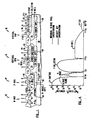
- Fig. 1 generally shows the structure resulting from the process of the present invention.
- a P-MOS transistor 14 and a vertical NPN transistor 16 which have been produced in the prior art
- the present invention also produces a vertical PNP transistor 18.
- a P substrate or P epitaxial layer 20 is first provided, and 3 N-wells 22, 24 and 26 are produced in step M #1 (see Appendix).
- N-Base 28 or PNP transistor 18 is then produced, followed by the implantation of the P-Base 30 for NPN transistor 16.
- the N+ source 32 and drain 34 of N-MOS transistor 12 are then produced, along with N+ emitter 36 of NPN transistor 16 and N+Base contact 38 of PNP transistor 18.
- the high energy implantation to produce P collector 40 is then done.
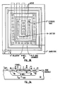
- PNP transistor 18 The preferred structure of PNP transistor 18 is shown in Figs. 2A and 2B in cross-sectional and top views, respectively. The numbering corresponds to that of Fig. 1. Also shown is an additional P+ region 52 for coupling to the P substrate 20 and an N+ region 54 for coupling to N well 26.
- Figs. 3A and 3B show a preferred embodiment of NPN transistor 16 of Fig. 1 with cross-sectional and top views, respectively. The numbering is the same as set forth in Fig. 1. In addition, an N+ collector contact 56 is shown.
- a high fT vertical PNP transistor is unique to this BiCMOS process. Details of fabrication of this device are now described.
- the usual implementation of high performance vertical PNP transistors involves complex process steps which reduce yield, such as double epitaxy, etc.
- a feature of the process described here is that it involves three (or two) additional masked implant steps only, i.e., an N-Base implant mask and a P-Collector implant mask. This gives two advantages:
- the P+ and N+ source/drain implants for the CMOS transistors form the P+ and N+ emitters of the PNP and NPN transistors, respectively.
- the N-well forms the collector of the NPN transistor and serves to isolate the P-collector of the PNP from the P-substrate or P-Epi on P-substrate.
- the N-well can merge with a N+ buried layer for higher NPN drive capability through a N+ buried layer implant and drive into a P-substrate and a subsequent P-Epi.
- the P-Base Implant for the NPN and P-Collector Implant of the PNP can be combined to eliminate one additional mask and implant reducing it to a 13 mask process. Therefore only the additional N-Base and P-Collector masked implant steps are explained here. The rest of the steps are same as in a conventional CMOS process.
- N-Base Phosphorus implant Simulations have been done for the optimum location of the N-Base Phosphorus implant in the process sequence. It is introduced early in the process, i.e., after the N-well drive and just prior to growing the gate oxide of the CMOS transistors. Thus, the N-Base is driven deep by subsequent thermal steps. If necessary, the drive can be increased without affecting the threshold adjust implants of the CMOS transistors, since these are implanted after the gate oxide. This deep drive gives a relatively flat implanted N-base impurity profile, leading to greater control and less sensivity to process variations, compared to a much steeper N-base profile if this implant were to be done later.
- the surface concentration of the implanted phosphorus must be less than 3E18/cc which corresponds to a typical dose of from 3E13 to 1.5E14/sq.cm.
- the N-Base implant dose and energy have a dominant influence on the following parameters:
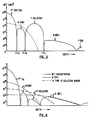
- the profile shown in Fig. 5 results from the process flow listed in the Appendix.
- the N-Base mask follows immediately after the Field implant.
- the implanted base is driven deep (to a depth of about 1.2um at a concentration of 1 x 10¹⁶/cm3) due to subsequent high temperature steps such as gate oxide, interpoly oxidation at 1140°c etc. Therefore, the base impurity profile is approximately constant or flat over the final N-Base region (0.25 t 0.45/um depth).
- it is not sensitive to the BPSG flow and reflow conditions since the thermal Dt's associated with these steps are so much smaller compared to other high temperature steps such as interpoly ox., etc.
- a relatively stable individual base profile results.
- the typical base implant dose is in the range of 3 x 10¹³ to 1 x 10¹⁴/cm2 with a surface concentration in the range of 5 x 10¹⁷ to 2 x 10¹⁸/cm3. This corresponds to BVEBO in the range of 10 to 4V, which is quite adequate.
- the final net base charge is affected by compensation due to the P+ emitter profile diffusing down from the top surface and the a P collector profile (a retrograde one achieved by a high energy Boron implant) "pinching" from below.
- the P-collector is implanted at a very high energy (greater than 150 kV, preferably 180-200 kV Boron implant by using doubly ionized Boron or greater than 300 keV using singly ionized Boron).
- the resultant peak lies at a depth of about 0.8um below the surface, forming a P+ buried collector well.
- the retrograde P-collector combines a low series resistance with a smaller collector-base junction capacitance due to reduced collector doping at the junction. To maintain this advantage, the profile must not be flattened by out-diffusion from subsequent thermal steps. Therefore, the implant is done just before the PSG/BPSG deposition and sees only the bare minimum thermal drive necessary for the doped oxide to flow.
- the masked P+ S/D implant is also done at this stage as shown in the Process Sequence Table (Appendix). For the same reason, this implant uses a Boron (BF2) species to give a shallower P+/N-base junction than would be given by a Boron implant at the same energy.
- BF2 Boron
- the peak of the P-Collector lies at a depth of 0.7 to 0.8um for an implant energy in the range of 380-400 keV and the P-Collector - N-well junction depth is about 1.2um.
- the typical P-Collector implant dose is in the range of 2 x 10¹³/cm ⁇ 2 to 2 x 10¹⁴/cm ⁇ 2.
- the lower limit is set by the conditions that it must be larger than the N-well dose and by the condition that the pinched (buried) collector sheet resistance must not be too large in order to reduce the Ic*Rc voltage drop. If the P-Collector dose is increased, due to the standard deviation of the implant and diffusion during BPSG flow and reflow, it counter dopes the N-Base and increases the base sheet resistance.
- the pinched collector sheet resistance varies from 1000 to 200 ohms/square. These are low enough that even a small geometry device can carry several milliamps of collector current before the C-B junction gets forward biased due to the IcRc drop.
- the peak of the collector implant lies only at a depth of 0.7um. Therefore, the N-Base/P-Collector junction depth must be less than 0.5um.
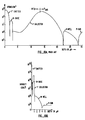
- a B11 Boron implant even at a low energy or 40 keV, has a large range and standard deviation so that the P+/N-Base junction depth is also approximately 0.5um. Therefore, as illustrated in Fig. 8, the P+ emitter and P-Collector merge.
- a P+ emitter implant using BF2 at a low energy of from 40 to 60 keV is much shallower. This is because BF2 dissociates into B11 and F2 on impact and the resultant B11 has energy of only 11/49 times the energy of the BF2 ion.
- a BF2 implant at 49 keV is equivalent to an 11 keV B ⁇ implant. Both the range and the standard deviation are therefore proportionately smaller, resulting in a shallower P+ emitter junction (0.25 to 0.3um). This as illustrated in Fig. 9, which shows the separation of the emitter from the P-Collector, allowing for an N-Base which is approximately 0-1 to 0-2um wide.
- the P+ emitter BF2 implant can also be replaced by a low energy Boron implant, i.e., B11 at less than 15 keV.
- the VPNP in the complementary bipolar processes is formed through a buried P+ collector through a P+ implant before epitaxy. This leads to larger size and process complications through auto doping due to the presence of both N+ and P+ buried layers.
- the P collector in the CB processes is formed, on other hand, by introducing a P+ buried layer, which in turn is isolated from the P- substrate by a very deep N-Well (junction depth of approx. 30um from the top surface and approx. 16um from the epi/substrate interface). Besides the increase in size, the deep buried P+ collector causes two significant process problems:
- the prior art process suffers from the same disadvantages common to other CB processes, i.e. large size due to deep junctions, simultaneous P+ and N+ buried layers and a very deep P-Well for isolation.
- Adding N+ Buried Layers The device described so far has been implemented in a conventional CMOS process.
- the collector series resistance In a BiCMOS process, to improve the drive capabilities of the vertical NPN, the collector series resistance must be reduced. This is done by incorporating an N+ buried layer 58 (see Fig. 1) in the front end.
Landscapes
- Metal-Oxide And Bipolar Metal-Oxide Semiconductor Integrated Circuits (AREA)
- Bipolar Transistors (AREA)
- Bipolar Integrated Circuits (AREA)
Claims (9)
- Verfahren zur Herstellung von CMOS-Transistoren und NPN-Transistoren auf einer einzigen Halbleiterscheibe, mit den Verfahrensschritten: Herstellung einer N-Wanne (24) als Kollektor eines vertikalen NPN-Transistors (16) und Herstellung eines isolierten, vertikalen PNP-Transistors (18), wobei Material vom Typ N zur Bildung einer N-Basis (28) des PNP-Transistors (18) implantiert wird, sowie Herstellung einer P-Region als Emitter des PNP-Transistors (18), dadurch gekennzeichnet,
daß während des Verfahrensschrittes zur Herstellung des Kollektors (24) des vertikalen NPN-Transistors eine N-Wanne (26) zur Aufnahme des PNP-Transistors (18) hergestellt wird,
und daß zur Herstellung des Kollektors des PNP-Transistors (18) Material vom Typ P implantiert wird mit einer Energie größer als 300 keV für einfach ionisiertes Material oder größer als 150 keV für doppelt ionisiertes Material. - Verfahren nach Anspruch 1,
dadurch gekennzeichnet, daß die N-Basis (28) mit einer Dosis von 3 x 10¹³/cm² bis 1,5 x 10¹⁴/cm² implantiert wird. - Verfahren nach Anspruch 2,
dadurch gekennzeichnet, daß das Material vom Typ N für die N-Basis (28) Phosphor ist. - Verfahren nach Anspruch 1,
dadurch gekennzeichnet, daß die N-Basis (28) zeitlich vor dem Kollektor des PNP-Transistors hergestellt wird. - Verfahren nach Anspruch 1,
dadurch gekennzeichnet, daß der Emitter des PNP-Transistors (18) eine flache P⁺-Region von weniger als 0,35 µm Dicke ist. - Verfahren nach Anspruch 1,
dadurch gekennzeichnet, daß das doppelt ionisierte Material Bor ist. - Verfahren nach Anspruch 1,
dadurch gekennzeichnet, daß der PNP-Emitter in demselben Verfahrensschritt hergestellt wird wie die Herstellung einer P⁺-Quelle und eines P⁺-Drain der CMOS-Transistoren. - Verfahren nach Anspruch 1,
dadurch gekennzeichnet, daß der PNP-Kollektor in demselben Verfahrensschritt hergestellt wird wie eine P-Basis (30) des NPN-Transistors. - Verfahren nach Anspruch 1,
gekennzeichnet durch die Verfahrensschritte:
Implantieren einer vergrabenen N⁺-Schicht (58) unter der N-Wanne (24); und
Züchten einer Epitaxieschicht (60) vom Typ P.
Priority Applications (1)
| Application Number | Priority Date | Filing Date | Title |
|---|---|---|---|
| AT89300019T ATE98815T1 (de) | 1988-01-21 | 1989-01-04 | Verfahren zum herstellen eines komplementaeren bicmos-transistors mit isoliertem vertikalem pnp- transistor. |
Applications Claiming Priority (2)
| Application Number | Priority Date | Filing Date | Title |
|---|---|---|---|
| US14693488A | 1988-01-21 | 1988-01-21 | |
| US146934 | 1988-01-21 |
Publications (3)
| Publication Number | Publication Date |
|---|---|
| EP0325342A2 EP0325342A2 (de) | 1989-07-26 |
| EP0325342A3 EP0325342A3 (en) | 1990-10-03 |
| EP0325342B1 true EP0325342B1 (de) | 1993-12-15 |
Family
ID=22519636
Family Applications (1)
| Application Number | Title | Priority Date | Filing Date |
|---|---|---|---|
| EP89300019A Expired - Lifetime EP0325342B1 (de) | 1988-01-21 | 1989-01-04 | Verfahren zum Herstellen eines komplementären BICMOS-Transistors mit isoliertem vertikalem PNP-Transistor |
Country Status (5)
| Country | Link |
|---|---|
| EP (1) | EP0325342B1 (de) |
| JP (1) | JPH0748530B2 (de) |
| KR (1) | KR910009337B1 (de) |
| AT (1) | ATE98815T1 (de) |
| DE (1) | DE68911321T2 (de) |
Cited By (1)
| Publication number | Priority date | Publication date | Assignee | Title |
|---|---|---|---|---|
| RU2106039C1 (ru) * | 1995-11-09 | 1998-02-27 | Акционерное общество открытого типа "НИИМЭ и завод "Микрон" | Способ изготовления бикмоп структур |
Families Citing this family (5)
| Publication number | Priority date | Publication date | Assignee | Title |
|---|---|---|---|---|
| KR940003589B1 (ko) * | 1991-02-25 | 1994-04-25 | 삼성전자 주식회사 | BiCMOS 소자의 제조 방법 |
| DE4411869C2 (de) * | 1994-04-06 | 1997-05-15 | Siemens Ag | Schaltungsanordnung mit einer integrierten Treiberschaltungsanordnung |
| RU2141149C1 (ru) * | 1998-07-09 | 1999-11-10 | Акционерное общество открытого типа "Научно-исследовательский институт молекулярной электроники и завод "Микрон" | Способ изготовления бикмоп структуры |
| RU2141148C1 (ru) * | 1998-07-09 | 1999-11-10 | Акционерное общество открытого типа "НИИМЭ и завод "Микрон" | Способ изготовления бикмоп прибора |
| DE19844531B4 (de) * | 1998-09-29 | 2017-12-14 | Prema Semiconductor Gmbh | Verfahren zur Herstellung von Transistoren |
Family Cites Families (3)
| Publication number | Priority date | Publication date | Assignee | Title |
|---|---|---|---|---|
| US4637125A (en) * | 1983-09-22 | 1987-01-20 | Kabushiki Kaisha Toshiba | Method for making a semiconductor integrated device including bipolar transistor and CMOS transistor |
| US4752589A (en) * | 1985-12-17 | 1988-06-21 | Siemens Aktiengesellschaft | Process for the production of bipolar transistors and complementary MOS transistors on a common silicon substrate |
| US4737472A (en) * | 1985-12-17 | 1988-04-12 | Siemens Aktiengesellschaft | Process for the simultaneous production of self-aligned bipolar transistors and complementary MOS transistors on a common silicon substrate |
-
1989
- 1989-01-04 DE DE68911321T patent/DE68911321T2/de not_active Expired - Fee Related
- 1989-01-04 AT AT89300019T patent/ATE98815T1/de not_active IP Right Cessation
- 1989-01-04 EP EP89300019A patent/EP0325342B1/de not_active Expired - Lifetime
- 1989-01-21 KR KR1019890000629A patent/KR910009337B1/ko not_active Expired
- 1989-01-21 JP JP1011014A patent/JPH0748530B2/ja not_active Expired - Lifetime
Cited By (1)
| Publication number | Priority date | Publication date | Assignee | Title |
|---|---|---|---|---|
| RU2106039C1 (ru) * | 1995-11-09 | 1998-02-27 | Акционерное общество открытого типа "НИИМЭ и завод "Микрон" | Способ изготовления бикмоп структур |
Also Published As
| Publication number | Publication date |
|---|---|
| JPH0748530B2 (ja) | 1995-05-24 |
| DE68911321D1 (de) | 1994-01-27 |
| EP0325342A2 (de) | 1989-07-26 |
| KR890012391A (ko) | 1989-08-26 |
| KR910009337B1 (ko) | 1991-11-11 |
| ATE98815T1 (de) | 1994-01-15 |
| JPH027462A (ja) | 1990-01-11 |
| DE68911321T2 (de) | 1994-07-07 |
| EP0325342A3 (en) | 1990-10-03 |
Similar Documents
| Publication | Publication Date | Title |
|---|---|---|
| US5011784A (en) | Method of making a complementary BiCMOS process with isolated vertical PNP transistors | |
| US5248624A (en) | Method of making isolated vertical pnp transistor in a complementary bicmos process with eeprom memory | |
| US4694562A (en) | Method for manufacturing a semiconductor integrated device including bipolar and CMOS transistors | |
| US4484388A (en) | Method for manufacturing semiconductor Bi-CMOS device | |
| US4734382A (en) | BiCMOS process having narrow bipolar emitter and implanted aluminum isolation | |
| US8603873B2 (en) | High-gain bipolar junction transistor compatible with complementary metal-oxide-semiconductor (CMOS) process and method for fabricating the same | |
| EP0139019B1 (de) | Halbleiteranordnung und deren herstellung | |
| US5679587A (en) | Method of fabricating an integrated circuit with vertical bipolar power transistors and isolated lateral bipolar control transistors | |
| US4902639A (en) | Process for making BiCMOS integrated circuit having a shallow trench bipolar transistor with vertical base contacts | |
| US5408125A (en) | Semiconductor process for manufacturing semiconductor device with increased operating voltages | |
| US5268312A (en) | Method of forming isolated wells in the fabrication of BiCMOS devices | |
| US5652456A (en) | Semiconductor structure containing multiple optimized well regions | |
| EP0569204B1 (de) | Verfahren zur Herstellung von N-Kanal- und P-Kanal-Sperrschicht-Feldeffekttransistoren unter Verwendung eines BiCMOS-Verfahrens | |
| EP0746038B1 (de) | Isolierter vertikaler PNP-Transistor und Verfahren zu seiner Herstellung | |
| US5455447A (en) | Vertical PNP transistor in merged bipolar/CMOS technology | |
| KR0166052B1 (ko) | 고전압 병합 바이폴라/cmos 및 그 제조 방법 | |
| EP0325342A2 (de) | Verfahren zum Herstellen eines komplementären BICMOS-Transistors mit isoliertem vertikalem PNP-Transistor | |
| US5786622A (en) | Bipolar transistor with a ring emitter | |
| US6359317B1 (en) | Vertical PNP bipolar transistor and its method of fabrication | |
| US6501152B1 (en) | Advanced lateral PNP by implant negation | |
| US6797577B2 (en) | One mask PNP (or NPN) transistor allowing high performance | |
| US6281530B1 (en) | LPNP utilizing base ballast resistor | |
| EP0348626B1 (de) | Verfahren zur Herstellung von isolierten vertikalbipolaren und JFET-Transistoren und entsprechender IC | |
| EP0792514B1 (de) | Herstellungsverfahren eines integrierten schaltkreises mit komplementären isolierten bipolartransistoren | |
| US6130122A (en) | Method for forming a BiCMOS integrated circuit with Nwell compensation implant and method |
Legal Events
| Date | Code | Title | Description |
|---|---|---|---|
| PUAI | Public reference made under article 153(3) epc to a published international application that has entered the european phase |
Free format text: ORIGINAL CODE: 0009012 |
|
| AK | Designated contracting states |
Kind code of ref document: A2 Designated state(s): AT DE FR GB IT NL |
|
| PUAL | Search report despatched |
Free format text: ORIGINAL CODE: 0009013 |
|
| AK | Designated contracting states |
Kind code of ref document: A3 Designated state(s): AT DE FR GB IT NL |
|
| 17P | Request for examination filed |
Effective date: 19901119 |
|
| 17Q | First examination report despatched |
Effective date: 19921012 |
|
| GRAA | (expected) grant |
Free format text: ORIGINAL CODE: 0009210 |
|
| AK | Designated contracting states |
Kind code of ref document: B1 Designated state(s): AT DE FR GB IT NL |
|
| REF | Corresponds to: |
Ref document number: 98815 Country of ref document: AT Date of ref document: 19940115 Kind code of ref document: T |
|
| REF | Corresponds to: |
Ref document number: 68911321 Country of ref document: DE Date of ref document: 19940127 |
|
| ITF | It: translation for a ep patent filed | ||
| ET | Fr: translation filed | ||
| PLBE | No opposition filed within time limit |
Free format text: ORIGINAL CODE: 0009261 |
|
| STAA | Information on the status of an ep patent application or granted ep patent |
Free format text: STATUS: NO OPPOSITION FILED WITHIN TIME LIMIT |
|
| 26N | No opposition filed | ||
| PGFP | Annual fee paid to national office [announced via postgrant information from national office to epo] |
Ref country code: AT Payment date: 19941216 Year of fee payment: 7 |
|
| PGFP | Annual fee paid to national office [announced via postgrant information from national office to epo] |
Ref country code: NL Payment date: 19950131 Year of fee payment: 7 |
|
| PG25 | Lapsed in a contracting state [announced via postgrant information from national office to epo] |
Ref country code: AT Effective date: 19960104 |
|
| PG25 | Lapsed in a contracting state [announced via postgrant information from national office to epo] |
Ref country code: NL Effective date: 19960801 |
|
| NLV4 | Nl: lapsed or anulled due to non-payment of the annual fee |
Effective date: 19960801 |
|
| PGFP | Annual fee paid to national office [announced via postgrant information from national office to epo] |
Ref country code: FR Payment date: 19981217 Year of fee payment: 11 |
|
| PGFP | Annual fee paid to national office [announced via postgrant information from national office to epo] |
Ref country code: GB Payment date: 19981218 Year of fee payment: 11 |
|
| PGFP | Annual fee paid to national office [announced via postgrant information from national office to epo] |
Ref country code: DE Payment date: 19981221 Year of fee payment: 11 |
|
| PG25 | Lapsed in a contracting state [announced via postgrant information from national office to epo] |
Ref country code: GB Free format text: LAPSE BECAUSE OF NON-PAYMENT OF DUE FEES Effective date: 20000104 |
|
| GBPC | Gb: european patent ceased through non-payment of renewal fee |
Effective date: 20000104 |
|
| PG25 | Lapsed in a contracting state [announced via postgrant information from national office to epo] |
Ref country code: FR Free format text: LAPSE BECAUSE OF NON-PAYMENT OF DUE FEES Effective date: 20000929 |
|
| PG25 | Lapsed in a contracting state [announced via postgrant information from national office to epo] |
Ref country code: DE Free format text: LAPSE BECAUSE OF NON-PAYMENT OF DUE FEES Effective date: 20001101 |
|
| REG | Reference to a national code |
Ref country code: FR Ref legal event code: ST |
|
| PG25 | Lapsed in a contracting state [announced via postgrant information from national office to epo] |
Ref country code: IT Free format text: LAPSE BECAUSE OF NON-PAYMENT OF DUE FEES Effective date: 20050104 |