EP0325423B1 - Circuit de détection d'erreur pour un décodeur - Google Patents
Circuit de détection d'erreur pour un décodeur Download PDFInfo
- Publication number
- EP0325423B1 EP0325423B1 EP89300436A EP89300436A EP0325423B1 EP 0325423 B1 EP0325423 B1 EP 0325423B1 EP 89300436 A EP89300436 A EP 89300436A EP 89300436 A EP89300436 A EP 89300436A EP 0325423 B1 EP0325423 B1 EP 0325423B1
- Authority
- EP
- European Patent Office
- Prior art keywords
- circuit
- node
- input node
- output
- units
- Prior art date
- Legal status (The legal status is an assumption and is not a legal conclusion. Google has not performed a legal analysis and makes no representation as to the accuracy of the status listed.)
- Expired - Lifetime
Links
Images


Classifications
-
- G—PHYSICS
- G06—COMPUTING OR CALCULATING; COUNTING
- G06F—ELECTRIC DIGITAL DATA PROCESSING
- G06F11/00—Error detection; Error correction; Monitoring
- G06F11/07—Responding to the occurrence of a fault, e.g. fault tolerance
- G06F11/0703—Error or fault processing not based on redundancy, i.e. by taking additional measures to deal with the error or fault not making use of redundancy in operation, in hardware, or in data representation
- G06F11/0751—Error or fault detection not based on redundancy
- G06F11/0763—Error or fault detection not based on redundancy by bit configuration check, e.g. of formats or tags
-
- G—PHYSICS
- G06—COMPUTING OR CALCULATING; COUNTING
- G06F—ELECTRIC DIGITAL DATA PROCESSING
- G06F11/00—Error detection; Error correction; Monitoring
- G06F11/07—Responding to the occurrence of a fault, e.g. fault tolerance
- G06F11/08—Error detection or correction by redundancy in data representation, e.g. by using checking codes
- G06F11/085—Error detection or correction by redundancy in data representation, e.g. by using checking codes using codes with inherent redundancy, e.g. n-out-of-m codes
Definitions
- the present invention relates to an error detecting circuit for a decoder having a plurality of output terminals and producing an active logic level at one output terminal in response to an input selection data.
- Such a decoder has been employed in a register selection circuit of a microprocessor or in a semiconductor memory as an address decoder.
- the decoder employed in the register selection circuit has a plurality of output terminals connected respectively to read/write enable terminals of a plurality of registers and outputs the active level to one of the output terminals in response to the selection data applied thereto, thus selecting a corresponding one of the registers. Data is thereby written into or read from the selected register.
- the active logic level is outputted at two or more output terminals in response to a single selection data. The corresponding two or more registers are thereby selected simultaneously, so that the contents stored in these registers are outputted simultaneously or the same data is written into two or more registers simultaneously.
- US-A-3.886.520 discloses a checking circuit for a 1-out-of- n decoder in which a binary table of rows and columns is established.
- Column associated 0-OR and 1-OR gates have their outputs coupled to ⁇ 1-OR and >1-OR gates to indicate that two or more, or none, of the decoder outputs is active.
- an object of the present invention is to provide a decoder error detecting circuit for detecting whether or not a decoder operates correctly.
- Another object of the present invention is to provide an error detection circuit for a decoder to detect whether or not two or more output terminals of the decoder take the active logic level in response to the same selection data.
- an error detection circuit for a decoder having a plurality of decoded output terminals, said error detection circuit comprising a set of first circuit units, each including a first input node, a first selection input node, a first output node, means for connecting said first input node to said first output node when said first selection input node is at a first logic level, and means for outputting a predetermined logic level to said first output node when said first selection input node is at a second logic level; a set of second circuit units, each including a second input node, a third input node, a second selection input node, a second output node, means for connecting said second input node to said second output node when said second selection input node is at said first logic level, and means for controlling a logic level of said second output node in response to the logic level of said third input node when second selection input node is at said second logic level; means connecting said first circuit units in series such that the first output node of the preced
- an error output signal is taken from the output terminal of the last series-connected second circuit unit.
- the associated two or more circuit units receive the active level at the respective selection input nodes.
- the first one of those associated circuit units outputs the predetermined logic level at its first output node, so that the second one of them outputs the predetermined logic level at its second output node.
- the predetermined logic level is propagated at the second output node of the last circuit unit, and the error detection signal is produced to indicate an incorrect operation of the decoder.
- the decoder may produce the active level at two or more output terminals in response to the same selection data
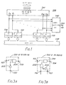
- a register selection circuit 500 includes a decoder 541 and sixteen registers 500 to 515.
- the decoder 541 has four input terminals I0 to I3 supplied with a 4-bits select data and sixteen output terminals O0 to O15 which are in turn connected to read/write enable terminals ET of the registers 500 to 515, respectively.
- an active level a high level or logic "1” in this description
- the remaining output terminals are held at an inactive level (i.e., a low level or logic "0").
- the decoder 541 fails or operates incorrectly, it outputs the active level at two or more output terminals thereof. For this reason, the corresponding two or more registers are selected and coupled to the data bus 539.
- an error detection circuit 540 is provided in accordance with the present invention. This circuit 540 is connected to the output terminals O0 to O15 of the decoder 541 and produces at a terminal 150 an error signal ERR when at least two output terminals of the decoder 541 take the active level simultaneously.
- the error detection circuit 540 includes fifteen first-type detecting circuits 120-0 to 120-14 and sixteen second-type detecting circuits 100-0 to 100-15.
- Each of the first-type detecting circuits 120-0 to 120-14 has an input node 121, an output node 123 and a selection input node 122.
- the selection nodes 122 of the detecting circuit 120-0 to 120-14 are connected to the first to fifteen output terminals O0 to O14 of the decoder 541, respectively.
- the first-type detecting circuits 120-0 to 120-14 are connected in series such that the output node 123 of the preceding circuit is connected to the input node 121 of the subsequent circuit.
- any one of the first-type detecting circuit 120-0 to 120-14 receives at its selection input node 122 the active level from the associated output terminal of the decoder 541, it produces the low level (logic "0") at its output node 123 irrespective of the logic level at its input node 121 to inform the subsequent detecting circuit 120 of receiving the active level from the decoder 541.
- the first-type detecting circuit or circuits 120 receiving the inactive level at the selection input node 122 transfer the logic level at the input node 121 to the output node 123. Since the detecting circuit 120-0 is the leading stage, the input node 121 thereof is fixed at logic "1" of Vcc level.
- Each of the second-type detecting circuits 100-0 to 100-15 has first and second input nodes 101 and 102, an output node 104 and a selection input node 103. These second-type detecting circuits 100-0 to 100-15 are connected in series such that the output node 104 of the preceding circuit is connected to the first input node 101 of the subsequent circuit.
- the selection input nodes 102 of the second-type detecting circuits 100-0 to 100-15 are connected to the output terminals O0 to O15 of the decoder 541, respectively.
- the second input nodes 102 of the second-type detecting circuits 100-1 to 100-15 except the leading circuit 100-0 are connected to the output nodes 123 of the first-type detecting circuits 120-0 to 120-14, respectively.
- the detecting circuit 100-0 Since the detecting circuit 100-0 is the leading circuit, the first and second input nodes 101 and 102 thereof are connected to Vcc terminal to receive logic "1".
- the second-type detecting circuit 100-0 to 100-15 receives at its selection input node 103 the active level from the associated output terminal of the decoder 541, it controls the logic level of its output node 104 in response to the logic level at its second input node 102.
- the output node 104 is controlled to be at the high level.
- the output node 104 In case where the second input node 102 is at the low level (logic "0"), the output node 104 is controlled to be at the low level.
- the second-type detecting circuit or circuits 100 receiving the inactive level at the selection node 103 from the decoder 541 transfer the logic level at the first input node 101 to the output node 104.
- An inverter 141 is connected between the error output terminal 150 and the final second-type detecting circuit 100-15. Therefore, the error detection signal ERR taking logic "1" indicates that the decoder 541 produces the active level at two or more output terminals simultaneously.
- the detecting circuit 120-1 thereby outputs logic "0" at its output node 123, so that more significant detecting circuits 120-2 to 120-14 also produce logic "0" at the respective output nodes 123. Only the circuit 120-0 produce logic "1" at its output node 123.
- the detecting circuit 100-1 responds the active level of the output terminal O1 to control its output node 104 in response to the logic level at its second input node 102.
- the error detection signal ERR takes logic "1" to indicate the incorrect operation of the decoder 541. More specifically, in response to the active level of the second output terminal O1, the output nodes 123 of the detecting circuit 120-1 to 120-14 all becomes to logic "0". Since the fifteenth output terminal O14 is also at the active level, the detecting circuit 100-14 controls the logic level of its output node 104 in response to the logic level at its second input node 102. Since logic "0" is applied thereto, the output node 104 of the detecting circuit 100-14 becomes to logic "0". This logic level, logic "0", is transferred to the inverter 141 via the circuit 100-15. As a result, the signal ERR takes logic "1".
- the error detection circuit 540 shown in Fig. 2 can be detect whether or not the decoder 541 operates correctly.
- Each of the first-type detecting circuit 120-0 to 120-14 and the second-type detecting circuits 100-0 to 100-15 having the above-mentioned functions can be constituted by various static-type and/or dynamic-type gate circuits.
- One example of each of the first-type detecting circuits 120-0 to 120-15 is shown in Fig. 3A and one example of each of the second-type detecting circuits 100-0 to 100-15 is shown in Fig. 3B.
- each of the first-type detecting circuits 120-0 to 120-14 includes an AND gate 204 and an inverter 205 which are connected as shown.
- each of the second-type detecting circuits 100-0 to 100-15 includes an OR gate 202, an AND gate 201 and an inverter 203 which are connected as shown. Therefore, when the node 103 receives the active level, the output node 104 is controlled by the logic level at the second input node 102. In case where the node 104 receives the inactive level, on the other hand, the AND gate 201 is made open to transfer the logic level at the first input node 101 to the output node 104.
- Fig. 4 Such an error detection circuit is shown in Fig. 4 as a second embodiment of the present invention, in which the same constituents as those shown in Fig. 1 are denoted by like reference numerals to omit the further description thereof.
- Fig. 4 a second set of sixteen second-type detecting circuits 100-16 to 100-31 are additionally provided and connected as shown, in cascade with the first set of second circuits 100-0 to 100-14.
- the inverter 141 is connected between the error detection output terminals 150 and the additionally provided sixteenth second-type detecting circuit 100-31.
- the signal ERR takes the logic "1" when the active level appears at three or more of decoded output terminals O0 to O15.
Landscapes
- Engineering & Computer Science (AREA)
- Theoretical Computer Science (AREA)
- Quality & Reliability (AREA)
- Physics & Mathematics (AREA)
- General Engineering & Computer Science (AREA)
- General Physics & Mathematics (AREA)
- Compression, Expansion, Code Conversion, And Decoders (AREA)
- Logic Circuits (AREA)
- For Increasing The Reliability Of Semiconductor Memories (AREA)
- Tests Of Electronic Circuits (AREA)
Claims (5)
- Circuit de détection d'erreur pour un décodeur ayant une multitude de bornes de sortie décodées (O₁ à O₁₅), le circuit de détection d'erreur comprenant :
un ensemble de premières unités de circuit (120-0 à 120-14), chacune comportant un premier noeud d'entrée (121), un premier noeud d'entrée de sélection (122), un premier noeud de sortie (123), un moyen pour connecter (204, 205) le premier noeud d'entrée (121) au premier noeud de sortie (123) lorsque le premier noeud d'entrée de sélection (122) est à un premier niveau logique, et un moyen pour sortir (204, 205) un niveau logique prédéterminé vers le premier noeud de sortie (123) lorsque le premier noeud d'entrée de sélection (122) est à un second niveau logique ;
un ensemble de secondes unités de circuit (100-0 à 100-15), chacune comportant un second noeud d'entrée (101), un troisième noeud d'entrée (102), un second noeud d'entrée de sélection (103), un second noeud de sortie (104), un moyen pour connecter (201, 202, 203) le second noeud d'entrée (101) au second noeud de sortie (104) lorsque le second noeud d'entrée de sélection (103) est au premier niveau logique, et un moyen pour commander (201, 202, 203) un niveau logique du second noeud de sortie (104) en réponse au niveau logique du troisième noeud d'entrée (102) lorsque le second noeud d'entrée de sélection (103) est au second niveau logique ;
un moyen connectant les premières unités de circuit (120-0 à 120-14) en série d'une manière telle que le premier noeud de sortie (123) de la première unité de circuit précédente est connecté au premier noeud d'entrée (121) de la première unité de circuit suivante ;
un moyen connectant les secondes unités de circuit (100-0 à 100-15) en série d'une manière telle que le second noeud de sortie (104) de la seconde unité de circuit précédente est connecté au second noeud d'entrée (101) de l'unité de circuit suivante ;
le premier noeud d'entrée (121) et le second noeud d'entrée (101) des première et seconde unités de circuit en tête étant respectivement connectés à un niveau logique fixe ;
un moyen connectant le premier noeud de sortie (123) de chacune des premières unités de circuit (120-0 à 120-14) au troisième noeud d'entrée (102) de l'unité associée des secondes unités de circuit (100-0 à 100-15) ;
un moyen connectant les premier et second noeuds d'entrée de sélection (122, 103) des premières et secondes unités de circuit (120-0 à 120-14, 100-0 à 100-15) à la borne correspondante des bornes de sortie décodées, et
un moyen connectant le troisième noeud d'entrée (102) de la seconde unité de circuit en tête desdites secondes unités de circuit (100-0 à 100-15) au premier noeud d'entrée (121) de la première unité de circuit en tête desdites premières unités de circuit. - Circuit de détection d'erreur selon la revendication 1, dans lequel un signal de sortie d'erreur (150) est prélevé à partir de la borne de sortie de la dernière des secondes unités de circuit connectées en série (100-15).
- Circuit de détection d'erreur selon la revendication 1, dans lequel il existe une multitude d'ensembles de secondes unités de circuit (100-0 à 100-15 et 100-16 à 100-31) disposées en cascade, les unités de chaque ensemble étant connectées en série l'une à l'autre et étant connectées aux unités de l'ensemble immédiatement en amont des premières unités de circuit ou des secondes unités de circuit de la manière spécifiée à la revendication 1 pour le premier ensemble mentionné des secondes unités de circuit, un signal de sortie d'erreur (150) étant prélevé à partir de la borne de sortie de la dernière unité de circuit parmi les secondes unités de circuit connectées en série (100-31) de l'ensemble le plus en aval des secondes unités de circuit.
- Circuit de détection d'erreur selon l'une quelconque des revendications précédentes, dans lequel chacune des premières unités de circuit (120-0 à 120-14) comporte un circuit ET (204) ayant une première borne d'entrée connectée au premier noeud d'entrée (121), une seconde borne d'entrée connectée par l'intermédiaire d'un premier inverseur (205) au premier noeud d'entrée de sélection (122) et une borne de sortie connectée au premier noeud de sortie (123).
- Circuit de détection d'erreur selon l'une quelconque des revendications précédentes, dans lequel chacune des secondes unités de circuit (100-0 à 100-15) comporte un circuit OU (202) et un circuit ET (201), le circuit OU (202) ayant une première borne d'entrée connectée au troisième noeud d'entrée (102) et une seconde borne d'entrée connectée par l'intermédiaire d'un second inverseur (203) au second noeud d'entrée de sélection (103), le circuit ET (201) ayant une première borne d'entrée connectée au second noeud d'entrée (101), une seconde borne d'entrée connectée à une borne de sortie du circuit OU (202) et une borne de sortie connectée au second noeud (104).
Applications Claiming Priority (2)
| Application Number | Priority Date | Filing Date | Title |
|---|---|---|---|
| JP63008765A JPH07120954B2 (ja) | 1988-01-18 | 1988-01-18 | デコーダのエラー検出回路 |
| JP8765/88 | 1988-01-18 |
Publications (3)
| Publication Number | Publication Date |
|---|---|
| EP0325423A2 EP0325423A2 (fr) | 1989-07-26 |
| EP0325423A3 EP0325423A3 (en) | 1990-03-21 |
| EP0325423B1 true EP0325423B1 (fr) | 1993-11-24 |
Family
ID=11702007
Family Applications (1)
| Application Number | Title | Priority Date | Filing Date |
|---|---|---|---|
| EP89300436A Expired - Lifetime EP0325423B1 (fr) | 1988-01-18 | 1989-01-18 | Circuit de détection d'erreur pour un décodeur |
Country Status (4)
| Country | Link |
|---|---|
| US (1) | US4949343A (fr) |
| EP (1) | EP0325423B1 (fr) |
| JP (1) | JPH07120954B2 (fr) |
| DE (1) | DE68910838T2 (fr) |
Families Citing this family (4)
| Publication number | Priority date | Publication date | Assignee | Title |
|---|---|---|---|---|
| JP2513514Y2 (ja) * | 1989-12-04 | 1996-10-09 | カシオ計算機株式会社 | デコ―ド回路 |
| JPH03189736A (ja) * | 1989-12-19 | 1991-08-19 | Nec Corp | 選択回路の障害検出方式 |
| GB9421552D0 (en) * | 1994-10-26 | 1994-12-14 | Philips Electronics Uk Ltd | Improvements in or relating to data communication |
| US5995016A (en) * | 1996-12-17 | 1999-11-30 | Rambus Inc. | Method and apparatus for N choose M device selection |
Family Cites Families (5)
| Publication number | Priority date | Publication date | Assignee | Title |
|---|---|---|---|---|
| US3744024A (en) * | 1972-01-03 | 1973-07-03 | Stromberg Carlson Corp | Circuit for detecting the presence of other than one-bit-out-of-n bits |
| US3886520A (en) * | 1974-04-03 | 1975-05-27 | Sperry Rand Corp | Checking circuit for a 1-out-of-n decoder |
| US4087786A (en) * | 1976-12-08 | 1978-05-02 | Bell Telephone Laboratories, Incorporated | One-bit-out-of-N-bit checking circuit |
| US4320512A (en) * | 1980-06-23 | 1982-03-16 | The Bendix Corporation | Monitored digital system |
| US4380813A (en) * | 1981-04-01 | 1983-04-19 | International Business Machines Corp. | Error checking of mutually-exclusive control signals |
-
1988
- 1988-01-18 JP JP63008765A patent/JPH07120954B2/ja not_active Expired - Lifetime
-
1989
- 1989-01-18 US US07/298,369 patent/US4949343A/en not_active Expired - Lifetime
- 1989-01-18 EP EP89300436A patent/EP0325423B1/fr not_active Expired - Lifetime
- 1989-01-18 DE DE89300436T patent/DE68910838T2/de not_active Expired - Fee Related
Also Published As
| Publication number | Publication date |
|---|---|
| EP0325423A3 (en) | 1990-03-21 |
| DE68910838D1 (de) | 1994-01-05 |
| DE68910838T2 (de) | 1994-03-17 |
| EP0325423A2 (fr) | 1989-07-26 |
| JPH07120954B2 (ja) | 1995-12-20 |
| US4949343A (en) | 1990-08-14 |
| JPH01183919A (ja) | 1989-07-21 |
Similar Documents
| Publication | Publication Date | Title |
|---|---|---|
| EP0540450B1 (fr) | Fonction CCE avec écriture partielle ou lecture/modification/écriture incorporée et schéma d'interfaçage avec parité anticipée | |
| EP0096782B1 (fr) | Réalignement on-line d'erreurs de mémoire | |
| EP0336435A2 (fr) | Dispositif et procédé de diagnostic de mémoire | |
| JPS6112292B2 (fr) | ||
| JPH01195557A (ja) | データ処理システムにおけるデータ転送方法 | |
| JPS62117200A (ja) | 自己テスト機能付き半導体メモリおよび自己テスト方法 | |
| US3898443A (en) | Memory fault correction system | |
| EP0096779A2 (fr) | Arrangement pour la dispersion d'erreur multibit afin de fournir une mémoire à semi-conducteur tolérant des défauts | |
| US20040205384A1 (en) | Computer system and memory control method thereof | |
| US4498178A (en) | Data error correction circuit | |
| EP0325423B1 (fr) | Circuit de détection d'erreur pour un décodeur | |
| JP2953737B2 (ja) | 複数ビット並列テスト回路を具備する半導体メモリ | |
| EP0189699A2 (fr) | Mémoire morte à lignes de bit interdigitales | |
| US4035766A (en) | Error-checking scheme | |
| KR100189531B1 (ko) | Cd-rom 드라이브에 있어서 섹터 데이타 디코딩방법 및 회로 | |
| JPS62242258A (ja) | 記憶装置 | |
| JPH07200419A (ja) | バスインタフェース装置 | |
| US5579269A (en) | Semiconductor memory device having redundancy serial access memory portion | |
| JPS58200351A (ja) | 誤り訂正回路 | |
| JPH0638239B2 (ja) | 誤り訂正機構 | |
| GB2158622A (en) | Computer controlled systems | |
| CA1182917A (fr) | Systeme de memoire utilisant des dispositifs de memoire a bulles defectueux | |
| JPH0760391B2 (ja) | 誤り訂正機構 | |
| JPH0227600A (ja) | 集積回路装置 | |
| JPS60163135A (ja) | デ−タバスチエツク方式 |
Legal Events
| Date | Code | Title | Description |
|---|---|---|---|
| PUAI | Public reference made under article 153(3) epc to a published international application that has entered the european phase |
Free format text: ORIGINAL CODE: 0009012 |
|
| 17P | Request for examination filed |
Effective date: 19890130 |
|
| AK | Designated contracting states |
Kind code of ref document: A2 Designated state(s): DE FR GB |
|
| PUAL | Search report despatched |
Free format text: ORIGINAL CODE: 0009013 |
|
| RHK1 | Main classification (correction) |
Ipc: H03M 13/02 |
|
| AK | Designated contracting states |
Kind code of ref document: A3 Designated state(s): DE FR GB |
|
| 17Q | First examination report despatched |
Effective date: 19920127 |
|
| GRAA | (expected) grant |
Free format text: ORIGINAL CODE: 0009210 |
|
| AK | Designated contracting states |
Kind code of ref document: B1 Designated state(s): DE FR GB |
|
| PG25 | Lapsed in a contracting state [announced via postgrant information from national office to epo] |
Ref country code: FR Effective date: 19931124 |
|
| REF | Corresponds to: |
Ref document number: 68910838 Country of ref document: DE Date of ref document: 19940105 |
|
| EN | Fr: translation not filed | ||
| PLBE | No opposition filed within time limit |
Free format text: ORIGINAL CODE: 0009261 |
|
| STAA | Information on the status of an ep patent application or granted ep patent |
Free format text: STATUS: NO OPPOSITION FILED WITHIN TIME LIMIT |
|
| 26N | No opposition filed | ||
| REG | Reference to a national code |
Ref country code: GB Ref legal event code: IF02 |
|
| PGFP | Annual fee paid to national office [announced via postgrant information from national office to epo] |
Ref country code: GB Payment date: 20020116 Year of fee payment: 14 |
|
| PGFP | Annual fee paid to national office [announced via postgrant information from national office to epo] |
Ref country code: DE Payment date: 20020227 Year of fee payment: 14 |
|
| PG25 | Lapsed in a contracting state [announced via postgrant information from national office to epo] |
Ref country code: GB Free format text: LAPSE BECAUSE OF NON-PAYMENT OF DUE FEES Effective date: 20030118 |
|
| PG25 | Lapsed in a contracting state [announced via postgrant information from national office to epo] |
Ref country code: DE Free format text: LAPSE BECAUSE OF NON-PAYMENT OF DUE FEES Effective date: 20030801 |
|
| GBPC | Gb: european patent ceased through non-payment of renewal fee |