EP0325427A2 - Vorrichtung zur Verbesserung einer Wellenform - Google Patents
Vorrichtung zur Verbesserung einer Wellenform Download PDFInfo
- Publication number
- EP0325427A2 EP0325427A2 EP89300444A EP89300444A EP0325427A2 EP 0325427 A2 EP0325427 A2 EP 0325427A2 EP 89300444 A EP89300444 A EP 89300444A EP 89300444 A EP89300444 A EP 89300444A EP 0325427 A2 EP0325427 A2 EP 0325427A2
- Authority
- EP
- European Patent Office
- Prior art keywords
- signal
- waveform
- full
- differentiation
- circuit
- Prior art date
- Legal status (The legal status is an assumption and is not a legal conclusion. Google has not performed a legal analysis and makes no representation as to the accuracy of the status listed.)
- Granted
Links
Images






Classifications
-
- H—ELECTRICITY
- H04—ELECTRIC COMMUNICATION TECHNIQUE
- H04N—PICTORIAL COMMUNICATION, e.g. TELEVISION
- H04N5/00—Details of television systems
- H04N5/14—Picture signal circuitry for video frequency region
- H04N5/142—Edging; Contouring
Definitions
- This invention relates to a waveform improving circuit for improving the waveform contour of a signal whose band is reduced such as, for example, a chrominance signal reproduced in a video tape recorder (VTR).
- VTR video tape recorder
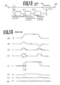
- Fig. 12 is a block diagram showing a conventional circuit for this purpose.
- Figs. 13(A) through (H) are diagrams showing the waveforms of signals of the circuit in Fig. 12. Referring to Fig. 12 and Figs. 13(A) through (H), a color difference signal a whose band is reduced is inputted to a terminal 30 and differentiated by a differentiation circuit 31 to be a signal b. The signal b thus obtained is subjected to a full-wave rectification by a full-wave rectification circuit 32 to be a signal c.
- the signal c thus obtained is waveform-shaped by a waveform shaping circuit 33 to be a signal d.
- the input signal a is subjected to sample-hold in response to this signal d by a sample-hold circuit 34 thereby to obtain an output signal e.
- the output signal e is improved in the contour of its waveform but a deviation of time t is taken place at the edge portion thereof.
- An object of the present invention is to provide a waveform improving apparatus which improves the waveform contour of a signal whose frequency band is reduced.
- a first input signal which is a signal to be improved in its waveform contour, is adjusted in its waveform such that a level at substantially the center of the rising slope of the waveform is raised to be substantially equal to a level at the uppermost end of the rising slope and that a level at substantially the center of the falling slope of the waveform is reduced to be substantially equal to a level at the lowermost end of the falling slope.
- a second signal which has a correlation to the first signal is differentiated twice to obtain two control pulses each having a predetermined pulse width - one of which terminates at a timing substantially corresponding to the center of the rising slope of the first signal waveform and the other of which terminates at a timing substantially corresponding to the center of the falling slope of the first signal waveform.
- the waveform-adjusted first signal is sampled at the leading edge of each of the two control pulses and the sampled level is held during the duration of each control pulse thereby obtaining a waveform contour improved first signal.
- the second signal may be the same as the first signal.
- the present invention is advantageously applicable to a video signal, which contains a luminance signal and a chrominance signal including a chrominance-difference signal, or which contains three primary color signals.
- the first signal may be a chrominance signal, and at this time the second signal may be either a luminance signal or the chrominance signal.
- Both the first and second signal may be a luminance signal.
- the first signal may be one of the three primary color signals, and at this time the second signal may be either the same as the first signal or another of the three primary color signals.
- the first and second signals may be selected such that they are correlated to each other.
- it is preferable to use a luminance signal as the second signal because the luminance signal generally has a high signal to noise ratio and a high frequency band. Both a luminance signal and a chrominance signal may be used for producing the control pulses.
- a waveform adjusting circuit for performing the waveform adjusting of the input first signal comprises: a differentiation circuit for differentiating the first signal; and an adder for adding the input first signal and an output of the differentiation circuit.
- a control pulse generating circuit for producing the control pulses from the second signal comprises: a first differentiation circuit for differentiating the input second signal; a full-wave rectification circuit for full-wave-rectifying an output of the first differentiation circuit; and a second differentiation circuit for differentiating an output of the full-wave rectification circuit.
- a waveform-adjusted first signal outputted from the waveform adjusting circuit is fed to a sample-and-hold circuit which is responsive to each control pulse outputted from the control pulse generating circuit for sampling and holding the waveform-adjusted first signal to obtain a waveform contour improved first signal.
- the waveform adjusting circuit may include a delay circuit for compensating a delay caused in the control pulse generating circuit.
- the control pulse generating circuit may include a waveform shaping circuit for shaping a pulse outputted from the second differentiation circuit into a rectangular waveform pulse.
- the control pulse generating circuit is provided before the first differentiation circuit with a low-pass filter for limiting the frequency band of the first signal so that each of the control pulses generated by the control pulse generating circuit has a proper pulse width.
- this low-pass filter may reduce the band of the second signal to be approximately the same as the band of the first signal.
- control pulse generating circuit may further comprise: a third differentiation circuit for differentiating the first signal; an additional full-wave rectification circuit for full-wave-rectifying an output of the third differentiation circuit; and an adder for adding outputs of the full-wave rectification circuit and the additional full-wave rectification circuit, an output of the adder being fed to the second differentiation circuit.
- This structure is advantageous in a case that the second signal is not always correlated to the first signal.
- This structure may be further modified such that a multiplier is provided between the first differentiation circuit and the full-wave rectification circuit for multiplying the outputs of the first and third differentiation circuits or between the full-wave rectification circuit and the adder for multiplying the outputs of the two full-wave rectification circuits.
- the multiplier operates as a kind of gate for passing the output of the first differentiation circuit to the second differentiation circuit only when there is a change in the first signal.
- control pulse generating circuit may have a gate circuit which is inserted to any position after the first differentiation circuit for passing the output information of the first differentiation circuit to the subsequent stage only when there is a change in the first signal.
- a circuit for detecting a change in the first signal is provided for producing a gate control signal for the gate circuit.
- the control pulse generating circuit may further comprises: an additional low-pass having a higher response than that of the low-pass filter provided before the first differentiation circuit for limitinng the band of the input second (luminance) signal; and additional differentiation circuit for differentiating an output of the additional low-pass filter; and an adder for adding outputs of the first and additional differentiation circuits, an output of the adder being fed to the full-wave rectification circuit.
- Fig. 1 is a block diagram showing a waveform improving apparatus in accordance with a first embodiment of this invention
- Fig. 2 shows waveforms of signals of the components of the circuit in Fig. 1.
- the reference letters (a) through (k) are designated correspondingly to each other. Since a video signal has a luminance signal and a color difference signal which are strongly correlated to each other, it may be considered that the luminance signal changes when the color difference signal changes. Therefore, in this first embodiment, a control signal f is obtained from the luminance signal.
- a luminance signal a inputted into a terminal 1 is sent to control signal generating circuit 3.
- the frequency band of the input signal is limited by a low-pass filter (LPF) 6 to be a signal b.
- the band-limited signal b is differentiated by a first differentiation circuit 7 to be a signal c.
- the signal c thus obtained is subjected to a full-wave rectification by a full-wave rectification circuit 8 to be a signal d.
- the signal d thus obtained is differentiated by a second differentiation circuit 9 to be a signal e.
- a waveform shaping circuit 10 detects a positive pulse portion of the signal c thus differentiated to obtain a control signal f.
- the control signal f thus obtained occurs from the beginning point of each edge slope part of the signal b to the center of the same.
- a color difference signal g (for example, R-Y or B-Y signal) is inputted to a terminal 2 and then fed to a waveform adjusting circuit 4.
- the color difference signal g is inputted to a delay circuit 11 which has a suitable delay time corresponding to a processing time in the control signal generating circuit 3, and, at the same time, inputted to a differentiation circuit 12.
- An output signal h of the differentiation circuit 12 is sliced at a small level by a slice circuit 13 in order to eliminate noise components thereby to obtain a signal i.
- the slice circuit 13 is not an inherently necessary circuit, and may be omitted.
- the signal i is added by an adder 14 with the output of the delay circuit 11 to obtain a signal j.
- the signal j thus obtained is subjected to sample-hold in response to the control signal f by a sample-hold circuit 5 to obtain a waveform contour improved signal k, which is outputted from a terminal 15.
- the waveform contour improving effect can be clearly seen by comparing the signal k with the input band-reduced signal g. In this case, if the output signal i of the slice circuit 13 is not added with the output of the delay circuit 11, the output signal k becomes as shown in l, so that the contour improving effect is halved. Therefore, it is preferable that the signal i is added with the output of the delay circuit 11 by the adder 14 so as to obtain the waveform of the signal k.
- the delay circuit 11 may be or may not be included in the waveform adjusting circuit 4.
- Fig. 2 (m) is a diagram schematically superposing the input signal g, the signal j and the output signal k. This clearly shows that the waveform contour is largely improved and yet no time delay at the edge portion of the output signal is generated.
- a waveform improving circuit of this invention achieves the waveform contour improving process of a signal at the center of each edge slope of the waveform thereof, which means that there is no time lag due to process.
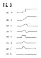
- the luminance signal is indicated as signal a.
- waveforms a through f as schematically illustrated in Figs. 3(A)-(E) are produced an consequently the signal to be outputted will become as shown at k.
- reference letters a through k in Fig. 3 correspond to the reference letters a through k in Fig. 1, respectively.
- the control signal f lasts almost through the interval of red, so that if sample-hold is made before the color difference signal indicates red an interval where the image is not colored is possibly generated. This is not preferable.
- a second embodiment of the control signal generating circuit 4 of the waveform improving circuit of this invention is shown in Fig. 4.
- a low-pass filter (LPF) 16 As clearly shown in Fig. 4 are disposed a low-pass filter (LPF) 16, a differentiation circuit 17 and an adder 18 additionally to the circuit shown in Fig. 1.
- the LPF 16 has a cut-off frequency which is higher than that of the LPF 6 shown in Fig. 1.
- the waveforms of signals of the components of the circuit in Fig. 4 are shown in Figs. 5(A) through (H), respectively.
- the luminance signal a is band-limited by the LPF 16 to be a signal b1 which is subsequently differentiated by the differentiation circuit 17 to be a signal c1.
- the differential signal c1 is added by the adder 18 to the differential signal c and rectified thereby to produce the signal d.
- the secondary differential signal becomes as an signal e and the control signal f is obtained.
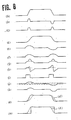
- Color difference output signals obtained when the color difference signal is subjected to the sample-hold by the signal f in Fig. 5 and the signal f in Fig. 3 are shown in Figs. 6(A) through (G), respectively.
- Fig. 6 In Fig. 6 are shown the luminance signal a, color difference signal g, added signal j, signal f1 which is identical to the signal f shown in Fig. 3, signal k1 which is produced by use of signal f1, signal f2 which is identical to the signal f shown in Fig. 5, and signal k2 which is produced by use of signal f2.
- signal k2 In the signal k2, such a decoloration as is seen in the case of the signal k1 is not generated.
- Fig. 7 is a block diagram showing a waveform improving apparatus in accordance with a third embodiment of the invention
- Fig. 8 shows waveforms of signals from the components of the apparatus in Fig. 7.
- Reference letters shown in Fig. 7 and Figs. 8(a) to (k) are designated correspondingly to each other.
- the control signal for improving the edge of a chrominance signal is made from the information on the change in chrominance signal is made from the information on the change in chrominance signal and the information on the change in luminance signal.
- a luminance signal a inputted to a terminal 1 is differentiated by a differentiation circuit 7 to obtain a signal b.
- a color difference signal d which is input to a terminal 2 is differentiated by a differentiation circuit 20 to obtain a signal e.
- the two signals b and c are subjected to full-wave rectification by full-wave rectification circuits 8 and 21 to obtain signals c and f, respectively.
- the signals c and f thus obtained are added by an adder 22 to output a signal g.
- the signal g is differentiated by a differentiation circuit 9 to output a signal h.
- the signal h is waveform-shaped by a waveform shaping circuit 10 thereby to obtain a control signal i.
- the luminance signal a is generally superior in S/N ratio to the color difference signal d, so that it is preferable that the control signal is obtained from the luminance signal.
- a video signal has no change in luminance signal but changes only in color difference signal
- it is impossible to generate the control signal which means that the waveform contour improvement is impossible to be achieved.
- the information on the luminance signal is used, and, on the other hand, when there exists no change in the luminance signal, the control signal is generated from the change in the color difference signal.
- This function is accomplished by the arrangement as shown in Fig. 7.
- a fourth embodiment of the control signal generating circuit is shown in Fig. 9.
- the differential signal b of the luminance signal a is fed to a gate circuit 23.
- the gate circuit 23 is controlled by the signal f which is obtained through the full-wave recification of the differential signal e of the color difference signal d.
- the gate circuit 23 is turned ON when the signal f becomes a specific output level.
- a control signal i is obtained using the information on the change in the luminance signal only when the color difference signal is being changed. This means that when the color difference signal has no change, no control signal is generated, so that such a malfunction that may execute a sample-hold at an unnecessary timing will be prevented from taking place.
- the gate circuit 23 can be insertedly disposed at any position in the path from the front of the full-wave rectification circuit 8 to the rear of the waveform shaping circuit 10 in Fig. 9.
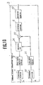
- a fifth embodiment of the control signal generating circuit is shown in Fig. 10 in a block diagram form.
- a multiplier 24 is used instead of the gate circuit 23 in Fig. 9 and an adder 22 is insertedly used successively thereto.
- the waveform contour of the color difference signal can be improved based on the change in the luminance signal which is superior in S/N ratio, and when there exists no correlation between the change in the luminance signal and the change in the color difference signal, the waveform contour is improved by the information on the change of the color difference signal itself.
- the delay circuit 11 in order to construct the waveform adjusting circuit 4, can be disposed at either front portion of the differentiation circuit 12 or rear portion of the adder 14 as shown in Figs. 11(A) and (B).
- the delay circuit in the waveform adjusting circuit 4 is not always necessary and may be omitted.
- the luminance signal and color difference signal are exemplified as the two input signals of the apparatus of this invention, but the two input signals may be identical to each other.
- both of the two input signals are a color difference signal or a luminance signal.
- the LPF 6 in the control signal generating circuit 3 shown in the first embodiment of this invention may be omitted.
Landscapes
- Engineering & Computer Science (AREA)
- Multimedia (AREA)
- Signal Processing (AREA)
- Picture Signal Circuits (AREA)
- Processing Of Color Television Signals (AREA)
Applications Claiming Priority (4)
| Application Number | Priority Date | Filing Date | Title |
|---|---|---|---|
| JP63008729A JP2523747B2 (ja) | 1988-01-19 | 1988-01-19 | 輪郭改善回路 |
| JP8729/88 | 1988-01-19 | ||
| JP8728/88 | 1988-01-19 | ||
| JP63008728A JP2523746B2 (ja) | 1988-01-19 | 1988-01-19 | 輪郭改善回路 |
Publications (3)
| Publication Number | Publication Date |
|---|---|
| EP0325427A2 true EP0325427A2 (de) | 1989-07-26 |
| EP0325427A3 EP0325427A3 (de) | 1991-07-03 |
| EP0325427B1 EP0325427B1 (de) | 1994-12-14 |
Family
ID=26343305
Family Applications (1)
| Application Number | Title | Priority Date | Filing Date |
|---|---|---|---|
| EP89300444A Expired - Lifetime EP0325427B1 (de) | 1988-01-19 | 1989-01-18 | Vorrichtung zur Verbesserung einer Wellenform |
Country Status (3)
| Country | Link |
|---|---|
| US (1) | US4931858A (de) |
| EP (1) | EP0325427B1 (de) |
| DE (1) | DE68919863T2 (de) |
Cited By (1)
| Publication number | Priority date | Publication date | Assignee | Title |
|---|---|---|---|---|
| US6008862A (en) * | 1996-09-16 | 1999-12-28 | U.S. Philips Corporation | Perceived color transient improvement |
Families Citing this family (9)
| Publication number | Priority date | Publication date | Assignee | Title |
|---|---|---|---|---|
| US5260774A (en) * | 1989-04-20 | 1993-11-09 | Canon Kabushiki Kaisha | White balance control for still image sensing apparatus |
| JPH0449781A (ja) * | 1990-06-19 | 1992-02-19 | Sony Corp | テレビジョン画像表示装置 |
| KR920008630B1 (ko) * | 1990-09-28 | 1992-10-02 | 삼성전자 주식회사 | 수평윤곽 보상회로 |
| DE19639572A1 (de) * | 1996-09-26 | 1998-04-02 | Philips Patentverwaltung | Verfahren und Anordnung zur Farbkantenversteilerung |
| US9174053B2 (en) | 2013-03-08 | 2015-11-03 | Boston Scientific Neuromodulation Corporation | Neuromodulation using modulated pulse train |
| CN106687173A (zh) * | 2014-09-15 | 2017-05-17 | 波士顿科学神经调制公司 | 用于对神经刺激脉冲模式进行编程的图形用户界面 |
| JP6452836B2 (ja) | 2014-11-04 | 2019-01-16 | ボストン サイエンティフィック ニューロモデュレイション コーポレイション | 複合神経刺激パターンをプログラムする方法及び装置 |
| EP3328481B1 (de) | 2015-07-30 | 2019-05-15 | Boston Scientific Neuromodulation Corporation | Benutzerschnittstelle für elektrische stimulation mit personalisiertem muster |
| US10456586B2 (en) | 2015-10-15 | 2019-10-29 | Boston Scientific Neuromodulation Corporation | User interface for neurostimulation waveform composition |
Family Cites Families (6)
| Publication number | Priority date | Publication date | Assignee | Title |
|---|---|---|---|---|
| DE2064731B2 (de) * | 1970-12-31 | 1973-06-07 | Robert Bosch Fernsehanlagen Gmbh, 6100 Darmstadt | Verfahren zur versteilerung von signalspruengen und schaltungsanordnung zur ausuebung des verfahrens |
| US4030121A (en) * | 1975-12-02 | 1977-06-14 | Faroudja Y C | Video crispener |
| US4181917A (en) * | 1977-07-01 | 1980-01-01 | Quadricolor Technology L.P. | Color television receiving system utilizing inferred high frequency signal components to reduce color infidelities in regions of color transitions |
| US4316215A (en) * | 1979-09-26 | 1982-02-16 | Matsushita Electric Industrial Co., Ltd. | System for improving reproduction of images in a color television receiver |
| US4331971A (en) * | 1980-11-19 | 1982-05-25 | Zenith Radio Corporation | Mode decision controller for selectively actuating a chrominance bandwith enhancement in a television receiver |
| DE3223580A1 (de) * | 1982-06-24 | 1983-12-29 | Philips Patentverwaltung Gmbh, 2000 Hamburg | Schaltungsanordnung zum erhoehen der schaerfe von farbkanten |
-
1989
- 1989-01-18 EP EP89300444A patent/EP0325427B1/de not_active Expired - Lifetime
- 1989-01-18 DE DE68919863T patent/DE68919863T2/de not_active Expired - Fee Related
- 1989-01-19 US US07/298,980 patent/US4931858A/en not_active Expired - Lifetime
Cited By (1)
| Publication number | Priority date | Publication date | Assignee | Title |
|---|---|---|---|---|
| US6008862A (en) * | 1996-09-16 | 1999-12-28 | U.S. Philips Corporation | Perceived color transient improvement |
Also Published As
| Publication number | Publication date |
|---|---|
| US4931858A (en) | 1990-06-05 |
| DE68919863D1 (de) | 1995-01-26 |
| DE68919863T2 (de) | 1995-07-06 |
| EP0325427A3 (de) | 1991-07-03 |
| EP0325427B1 (de) | 1994-12-14 |
Similar Documents
| Publication | Publication Date | Title |
|---|---|---|
| US4072984A (en) | Chrominance-luminance separator | |
| US4084181A (en) | Apparatus for transmission of chrominance signals during blanking period | |
| EP0084241B1 (de) | Gerät zur Signalverarbeitung und Verfahren zum Aufzeichnen auf einem Videoband | |
| US4015076A (en) | Noise eliminating circuit for video television signal | |
| EP0617564A2 (de) | Schaltung zur automatischen Signaltrennungsanpassung in ein Y/C Trennkammfilter | |
| US4931858A (en) | Waveform improving apparatus | |
| US4563704A (en) | Noise reduction circuit for a video signal | |
| CA2047398C (en) | Luminance signal noise suppressor | |
| GB1584317A (en) | Electronic time base error correction methods and arrangements | |
| US4293869A (en) | Circuit for reducing drop-out errors in a video signal derived from a recording device | |
| CA1115412A (en) | Suppression of luminance signal contamination of chrominance signals in a video signal processing system | |
| EP0199602B1 (de) | Signalverarbeitungsschaltung | |
| JP2523746B2 (ja) | 輪郭改善回路 | |
| US4101940A (en) | Circuit for delaying a composite video signal by a line duration, particularly for use with a video record player | |
| DE69604107T2 (de) | Farbsignaldemodulator geeignet für PAL- und SECAM-Fernsehempfänger | |
| EP0420184B1 (de) | Videosignalverarbeitungsschaltung | |
| EP0668702B1 (de) | Schaltung zur Trennung des Helligkeitssignals von einem Farbsignal | |
| US2844646A (en) | Television test apparatus | |
| US5159439A (en) | Circuit for controlling delay time between luminance and chrominance signals | |
| JP2523747B2 (ja) | 輪郭改善回路 | |
| JP3077154B2 (ja) | エンハンサ回路 | |
| SU1390817A1 (ru) | Устройство дл коррекции цветовых переходов | |
| JP2523745B2 (ja) | 輪郭改善回路 | |
| JPS57199386A (en) | Color video signal recording system and reproducing system | |
| JPH02149070A (ja) | 輪郭改善回路 |
Legal Events
| Date | Code | Title | Description |
|---|---|---|---|
| PUAI | Public reference made under article 153(3) epc to a published international application that has entered the european phase |
Free format text: ORIGINAL CODE: 0009012 |
|
| AK | Designated contracting states |
Kind code of ref document: A2 Designated state(s): DE FR GB |
|
| PUAL | Search report despatched |
Free format text: ORIGINAL CODE: 0009013 |
|
| AK | Designated contracting states |
Kind code of ref document: A3 Designated state(s): DE FR GB |
|
| 17P | Request for examination filed |
Effective date: 19911218 |
|
| 17Q | First examination report despatched |
Effective date: 19931007 |
|
| GRAA | (expected) grant |
Free format text: ORIGINAL CODE: 0009210 |
|
| AK | Designated contracting states |
Kind code of ref document: B1 Designated state(s): DE FR GB |
|
| REF | Corresponds to: |
Ref document number: 68919863 Country of ref document: DE Date of ref document: 19950126 |
|
| ET | Fr: translation filed | ||
| PLBE | No opposition filed within time limit |
Free format text: ORIGINAL CODE: 0009261 |
|
| STAA | Information on the status of an ep patent application or granted ep patent |
Free format text: STATUS: NO OPPOSITION FILED WITHIN TIME LIMIT |
|
| 26N | No opposition filed | ||
| REG | Reference to a national code |
Ref country code: GB Ref legal event code: IF02 |
|
| PGFP | Annual fee paid to national office [announced via postgrant information from national office to epo] |
Ref country code: FR Payment date: 20020110 Year of fee payment: 14 |
|
| PGFP | Annual fee paid to national office [announced via postgrant information from national office to epo] |
Ref country code: GB Payment date: 20020116 Year of fee payment: 14 |
|
| PGFP | Annual fee paid to national office [announced via postgrant information from national office to epo] |
Ref country code: DE Payment date: 20020227 Year of fee payment: 14 |
|
| PG25 | Lapsed in a contracting state [announced via postgrant information from national office to epo] |
Ref country code: GB Free format text: LAPSE BECAUSE OF NON-PAYMENT OF DUE FEES Effective date: 20030118 |
|
| PG25 | Lapsed in a contracting state [announced via postgrant information from national office to epo] |
Ref country code: DE Free format text: LAPSE BECAUSE OF NON-PAYMENT OF DUE FEES Effective date: 20030801 |
|
| GBPC | Gb: european patent ceased through non-payment of renewal fee | ||
| PG25 | Lapsed in a contracting state [announced via postgrant information from national office to epo] |
Ref country code: FR Free format text: LAPSE BECAUSE OF NON-PAYMENT OF DUE FEES Effective date: 20030930 |
|
| REG | Reference to a national code |
Ref country code: FR Ref legal event code: ST |