EP0326018A2 - Dispositif semi-conducteur comprenant des couches conductrices - Google Patents
Dispositif semi-conducteur comprenant des couches conductrices Download PDFInfo
- Publication number
- EP0326018A2 EP0326018A2 EP89100865A EP89100865A EP0326018A2 EP 0326018 A2 EP0326018 A2 EP 0326018A2 EP 89100865 A EP89100865 A EP 89100865A EP 89100865 A EP89100865 A EP 89100865A EP 0326018 A2 EP0326018 A2 EP 0326018A2
- Authority
- EP
- European Patent Office
- Prior art keywords
- conductor
- palladium
- semiconductor device
- conductor film
- substrate
- Prior art date
- Legal status (The legal status is an assumption and is not a legal conclusion. Google has not performed a legal analysis and makes no representation as to the accuracy of the status listed.)
- Granted
Links
Images


Classifications
-
- H—ELECTRICITY
- H10—SEMICONDUCTOR DEVICES; ELECTRIC SOLID-STATE DEVICES NOT OTHERWISE PROVIDED FOR
- H10W—GENERIC PACKAGES, INTERCONNECTIONS, CONNECTORS OR OTHER CONSTRUCTIONAL DETAILS OF DEVICES COVERED BY CLASS H10
- H10W20/00—Interconnections in chips, wafers or substrates
- H10W20/01—Manufacture or treatment
- H10W20/031—Manufacture or treatment of conductive parts of the interconnections
- H10W20/064—Manufacture or treatment of conductive parts of the interconnections by modifying the conductivity of conductive parts, e.g. by alloying
-
- H—ELECTRICITY
- H10—SEMICONDUCTOR DEVICES; ELECTRIC SOLID-STATE DEVICES NOT OTHERWISE PROVIDED FOR
- H10D—INORGANIC ELECTRIC SEMICONDUCTOR DEVICES
- H10D64/00—Electrodes of devices having potential barriers
- H10D64/01—Manufacture or treatment
- H10D64/011—Manufacture or treatment of electrodes ohmically coupled to a semiconductor
- H10D64/0111—Manufacture or treatment of electrodes ohmically coupled to a semiconductor to Group IV semiconductors
- H10D64/0112—Manufacture or treatment of electrodes ohmically coupled to a semiconductor to Group IV semiconductors using conductive layers comprising silicides
-
- H—ELECTRICITY
- H10—SEMICONDUCTOR DEVICES; ELECTRIC SOLID-STATE DEVICES NOT OTHERWISE PROVIDED FOR
- H10P—GENERIC PROCESSES OR APPARATUS FOR THE MANUFACTURE OR TREATMENT OF DEVICES COVERED BY CLASS H10
- H10P50/00—Etching of wafers, substrates or parts of devices
- H10P50/20—Dry etching; Plasma etching; Reactive-ion etching
- H10P50/26—Dry etching; Plasma etching; Reactive-ion etching of conductive or resistive materials
- H10P50/264—Dry etching; Plasma etching; Reactive-ion etching of conductive or resistive materials by chemical means
- H10P50/266—Dry etching; Plasma etching; Reactive-ion etching of conductive or resistive materials by chemical means by vapour etching only
- H10P50/267—Dry etching; Plasma etching; Reactive-ion etching of conductive or resistive materials by chemical means by vapour etching only using plasmas
-
- H—ELECTRICITY
- H10—SEMICONDUCTOR DEVICES; ELECTRIC SOLID-STATE DEVICES NOT OTHERWISE PROVIDED FOR
- H10W—GENERIC PACKAGES, INTERCONNECTIONS, CONNECTORS OR OTHER CONSTRUCTIONAL DETAILS OF DEVICES COVERED BY CLASS H10
- H10W20/00—Interconnections in chips, wafers or substrates
- H10W20/01—Manufacture or treatment
- H10W20/031—Manufacture or treatment of conductive parts of the interconnections
- H10W20/064—Manufacture or treatment of conductive parts of the interconnections by modifying the conductivity of conductive parts, e.g. by alloying
- H10W20/065—Manufacture or treatment of conductive parts of the interconnections by modifying the conductivity of conductive parts, e.g. by alloying by making at least a portion of the conductive part non-conductive, e.g. by oxidation
-
- H—ELECTRICITY
- H10—SEMICONDUCTOR DEVICES; ELECTRIC SOLID-STATE DEVICES NOT OTHERWISE PROVIDED FOR
- H10W—GENERIC PACKAGES, INTERCONNECTIONS, CONNECTORS OR OTHER CONSTRUCTIONAL DETAILS OF DEVICES COVERED BY CLASS H10
- H10W20/00—Interconnections in chips, wafers or substrates
- H10W20/40—Interconnections external to wafers or substrates, e.g. back-end-of-line [BEOL] metallisations or vias connecting to gate electrodes
- H10W20/41—Interconnections external to wafers or substrates, e.g. back-end-of-line [BEOL] metallisations or vias connecting to gate electrodes characterised by their conductive parts
- H10W20/425—Barrier, adhesion or liner layers
-
- H—ELECTRICITY
- H10—SEMICONDUCTOR DEVICES; ELECTRIC SOLID-STATE DEVICES NOT OTHERWISE PROVIDED FOR
- H10W—GENERIC PACKAGES, INTERCONNECTIONS, CONNECTORS OR OTHER CONSTRUCTIONAL DETAILS OF DEVICES COVERED BY CLASS H10
- H10W20/00—Interconnections in chips, wafers or substrates
- H10W20/40—Interconnections external to wafers or substrates, e.g. back-end-of-line [BEOL] metallisations or vias connecting to gate electrodes
- H10W20/41—Interconnections external to wafers or substrates, e.g. back-end-of-line [BEOL] metallisations or vias connecting to gate electrodes characterised by their conductive parts
- H10W20/44—Conductive materials thereof
- H10W20/4403—Conductive materials thereof based on metals, e.g. alloys, metal silicides
- H10W20/4405—Conductive materials thereof based on metals, e.g. alloys, metal silicides the principal metal being aluminium
- H10W20/4407—Aluminium alloys
-
- H—ELECTRICITY
- H10—SEMICONDUCTOR DEVICES; ELECTRIC SOLID-STATE DEVICES NOT OTHERWISE PROVIDED FOR
- H10W—GENERIC PACKAGES, INTERCONNECTIONS, CONNECTORS OR OTHER CONSTRUCTIONAL DETAILS OF DEVICES COVERED BY CLASS H10
- H10W70/00—Package substrates; Interposers; Redistribution layers [RDL]
- H10W70/60—Insulating or insulated package substrates; Interposers; Redistribution layers
-
- H—ELECTRICITY
- H10—SEMICONDUCTOR DEVICES; ELECTRIC SOLID-STATE DEVICES NOT OTHERWISE PROVIDED FOR
- H10W—GENERIC PACKAGES, INTERCONNECTIONS, CONNECTORS OR OTHER CONSTRUCTIONAL DETAILS OF DEVICES COVERED BY CLASS H10
- H10W72/00—Interconnections or connectors in packages
- H10W72/50—Bond wires
- H10W72/531—Shapes of wire connectors
- H10W72/536—Shapes of wire connectors the connected ends being ball-shaped
-
- H—ELECTRICITY
- H10—SEMICONDUCTOR DEVICES; ELECTRIC SOLID-STATE DEVICES NOT OTHERWISE PROVIDED FOR
- H10W—GENERIC PACKAGES, INTERCONNECTIONS, CONNECTORS OR OTHER CONSTRUCTIONAL DETAILS OF DEVICES COVERED BY CLASS H10
- H10W72/00—Interconnections or connectors in packages
- H10W72/50—Bond wires
- H10W72/531—Shapes of wire connectors
- H10W72/5363—Shapes of wire connectors the connected ends being wedge-shaped
-
- H—ELECTRICITY
- H10—SEMICONDUCTOR DEVICES; ELECTRIC SOLID-STATE DEVICES NOT OTHERWISE PROVIDED FOR
- H10W—GENERIC PACKAGES, INTERCONNECTIONS, CONNECTORS OR OTHER CONSTRUCTIONAL DETAILS OF DEVICES COVERED BY CLASS H10
- H10W72/00—Interconnections or connectors in packages
- H10W72/50—Bond wires
- H10W72/551—Materials of bond wires
- H10W72/552—Materials of bond wires comprising metals or metalloids, e.g. silver
- H10W72/5522—Materials of bond wires comprising metals or metalloids, e.g. silver comprising gold [Au]
-
- H—ELECTRICITY
- H10—SEMICONDUCTOR DEVICES; ELECTRIC SOLID-STATE DEVICES NOT OTHERWISE PROVIDED FOR
- H10W—GENERIC PACKAGES, INTERCONNECTIONS, CONNECTORS OR OTHER CONSTRUCTIONAL DETAILS OF DEVICES COVERED BY CLASS H10
- H10W72/00—Interconnections or connectors in packages
- H10W72/50—Bond wires
- H10W72/551—Materials of bond wires
- H10W72/552—Materials of bond wires comprising metals or metalloids, e.g. silver
- H10W72/5524—Materials of bond wires comprising metals or metalloids, e.g. silver comprising aluminium [Al]
-
- H—ELECTRICITY
- H10—SEMICONDUCTOR DEVICES; ELECTRIC SOLID-STATE DEVICES NOT OTHERWISE PROVIDED FOR
- H10W—GENERIC PACKAGES, INTERCONNECTIONS, CONNECTORS OR OTHER CONSTRUCTIONAL DETAILS OF DEVICES COVERED BY CLASS H10
- H10W72/00—Interconnections or connectors in packages
- H10W72/50—Bond wires
- H10W72/551—Materials of bond wires
- H10W72/552—Materials of bond wires comprising metals or metalloids, e.g. silver
- H10W72/5525—Materials of bond wires comprising metals or metalloids, e.g. silver comprising copper [Cu]
-
- H—ELECTRICITY
- H10—SEMICONDUCTOR DEVICES; ELECTRIC SOLID-STATE DEVICES NOT OTHERWISE PROVIDED FOR
- H10W—GENERIC PACKAGES, INTERCONNECTIONS, CONNECTORS OR OTHER CONSTRUCTIONAL DETAILS OF DEVICES COVERED BY CLASS H10
- H10W72/00—Interconnections or connectors in packages
- H10W72/851—Dispositions of multiple connectors or interconnections
- H10W72/874—On different surfaces
- H10W72/884—Die-attach connectors and bond wires
-
- H—ELECTRICITY
- H10—SEMICONDUCTOR DEVICES; ELECTRIC SOLID-STATE DEVICES NOT OTHERWISE PROVIDED FOR
- H10W—GENERIC PACKAGES, INTERCONNECTIONS, CONNECTORS OR OTHER CONSTRUCTIONAL DETAILS OF DEVICES COVERED BY CLASS H10
- H10W74/00—Encapsulations, e.g. protective coatings
-
- H—ELECTRICITY
- H10—SEMICONDUCTOR DEVICES; ELECTRIC SOLID-STATE DEVICES NOT OTHERWISE PROVIDED FOR
- H10W—GENERIC PACKAGES, INTERCONNECTIONS, CONNECTORS OR OTHER CONSTRUCTIONAL DETAILS OF DEVICES COVERED BY CLASS H10
- H10W90/00—Package configurations
- H10W90/701—Package configurations characterised by the relative positions of pads or connectors relative to package parts
- H10W90/731—Package configurations characterised by the relative positions of pads or connectors relative to package parts of die-attach connectors
- H10W90/736—Package configurations characterised by the relative positions of pads or connectors relative to package parts of die-attach connectors between a chip and a stacked lead frame, conducting package substrate or heat sink
-
- H—ELECTRICITY
- H10—SEMICONDUCTOR DEVICES; ELECTRIC SOLID-STATE DEVICES NOT OTHERWISE PROVIDED FOR
- H10W—GENERIC PACKAGES, INTERCONNECTIONS, CONNECTORS OR OTHER CONSTRUCTIONAL DETAILS OF DEVICES COVERED BY CLASS H10
- H10W90/00—Package configurations
- H10W90/701—Package configurations characterised by the relative positions of pads or connectors relative to package parts
- H10W90/751—Package configurations characterised by the relative positions of pads or connectors relative to package parts of bond wires
- H10W90/756—Package configurations characterised by the relative positions of pads or connectors relative to package parts of bond wires between a chip and a stacked lead frame, conducting package substrate or heat sink
-
- Y—GENERAL TAGGING OF NEW TECHNOLOGICAL DEVELOPMENTS; GENERAL TAGGING OF CROSS-SECTIONAL TECHNOLOGIES SPANNING OVER SEVERAL SECTIONS OF THE IPC; TECHNICAL SUBJECTS COVERED BY FORMER USPC CROSS-REFERENCE ART COLLECTIONS [XRACs] AND DIGESTS
- Y10—TECHNICAL SUBJECTS COVERED BY FORMER USPC
- Y10T—TECHNICAL SUBJECTS COVERED BY FORMER US CLASSIFICATION
- Y10T428/00—Stock material or miscellaneous articles
- Y10T428/12—All metal or with adjacent metals
- Y10T428/12493—Composite; i.e., plural, adjacent, spatially distinct metal components [e.g., layers, joint, etc.]
- Y10T428/12528—Semiconductor component
-
- Y—GENERAL TAGGING OF NEW TECHNOLOGICAL DEVELOPMENTS; GENERAL TAGGING OF CROSS-SECTIONAL TECHNOLOGIES SPANNING OVER SEVERAL SECTIONS OF THE IPC; TECHNICAL SUBJECTS COVERED BY FORMER USPC CROSS-REFERENCE ART COLLECTIONS [XRACs] AND DIGESTS
- Y10—TECHNICAL SUBJECTS COVERED BY FORMER USPC
- Y10T—TECHNICAL SUBJECTS COVERED BY FORMER US CLASSIFICATION
- Y10T428/00—Stock material or miscellaneous articles
- Y10T428/12—All metal or with adjacent metals
- Y10T428/12493—Composite; i.e., plural, adjacent, spatially distinct metal components [e.g., layers, joint, etc.]
- Y10T428/12535—Composite; i.e., plural, adjacent, spatially distinct metal components [e.g., layers, joint, etc.] with additional, spatially distinct nonmetal component
- Y10T428/12611—Oxide-containing component
-
- Y—GENERAL TAGGING OF NEW TECHNOLOGICAL DEVELOPMENTS; GENERAL TAGGING OF CROSS-SECTIONAL TECHNOLOGIES SPANNING OVER SEVERAL SECTIONS OF THE IPC; TECHNICAL SUBJECTS COVERED BY FORMER USPC CROSS-REFERENCE ART COLLECTIONS [XRACs] AND DIGESTS
- Y10—TECHNICAL SUBJECTS COVERED BY FORMER USPC
- Y10T—TECHNICAL SUBJECTS COVERED BY FORMER US CLASSIFICATION
- Y10T428/00—Stock material or miscellaneous articles
- Y10T428/12—All metal or with adjacent metals
- Y10T428/12493—Composite; i.e., plural, adjacent, spatially distinct metal components [e.g., layers, joint, etc.]
- Y10T428/12535—Composite; i.e., plural, adjacent, spatially distinct metal components [e.g., layers, joint, etc.] with additional, spatially distinct nonmetal component
- Y10T428/12625—Free carbon containing component
Definitions
- This invention relates to a semiconductor device, and particularly to a conductor film and fabricating method thereof applied suitably to large scale integration (LSI) circuit devices.
- LSI large scale integration
- the conductor of semiconductor device is generally made of aluminum added by several percent of silicon.
- the current flowing in the aluminum conductor film causes atoms of the film to move, resulting in the formation of hillocks in one section and voids in other section of the conductor film.
- a grown hillcock causes a short-circuit between interconnecting conductors. While a grown void causes an increased resistance of conductor at the portion of void and eventually a failure of conductor by heat generation, and both cases result in a malfunctioning of the semiconductor device.
- 0.1-54 weight-% of copper is added to aluminum so that a precipitation structure of CuAl2 particles is formed.
- the particles precipitate at grain boundaries and grain boundary triple points of the aluminum matrix to prevent the movement of aluminum atoms, and consequently the semiconductor device can have an extended life against electromigration.
- CuAl2 is highly apt to segregate, and the semiconductor device suffers a premature failure due to electromigration at portions where CuAl2 is not precipitated.
- Al-Cu alloy exhibits difficulty in fine pattern formation using dry etching, and is corroded severely by Cl and residual Cl ⁇ ion during the process, and therefore it is extremely difficult to have a forming accuracy of 1 ⁇ m or submicron pattern.
- Another problem in the operation of the semiconductor device is the reliability under humidity conditions.
- the Al conductor film is coated with a passivation film for surface protection, which exerts a tensional stress on the conductor film until it is broken, and this defect caused by so-called stress migration is also a problem.
- the Al-Cu conductor which has a poor pattern accuracy, is prone to break at a narrow portion.
- Japanese Patent Unexamined Publication JP-A-60-26640 discloses conductor materials consisting of aluminum, precious metals (Pt, Pd, Rh, Ir) and silicon
- another Japanese Patent Unexamined Publication JP-A-61-144847 discloses a semiconductor device having a conductor film formed of alloy including at least one of Pd and Pt by 0.1-2 weight-% and precipitated in the form of metal or compound. These wiring film materials are deposited on a semiconductor substrate by evapolative deposition or sputtering, and then formed into an intended pattern mainly by the wet-etching process.
- the inventors of the present invention has found the fact that when an aluminum conductor film or aluminum-based alloy conductor film including a small quantity of precious metal, silicon, copper, etc. added to aluminum is subjected to dry etching, the conductor film has its side wall etched slantwise (will be termed "side etching"), creating a difference in the pattern profile between the top and bottom line width.
- side etching side wall etched slantwise
- wet etching is free from the side etching problem, it is merely capable of forming lines down to several ⁇ m at most and is not suited for fine pattern formation of 1 ⁇ m or smaller.
- the line width of conductor film has come to be narrower, and the etching technique capable of pattern formation with a line width of 1.3 ⁇ m or less would be increasingly important.
- An object of this invention is to provide a method of fabricating a semiconductor device having a conductor film on a semiconductor substrate, in which the occurrence of side etching in the dry etching process of conductor film is prevented.
- Another object of this invention is to provide a semiconductor device having on its semiconductor substrate a conductor film for which the occurrence of side etching is prevented or significantly etching
- a further object of this invention is to provide a semiconductor device having its conductor film prevented or significantly controlled from the occurrence of side etching thereby to accomplish the fine conductor formation.
- a further object of this invention is to provice a semiconductor device and a fabricating method thereof having the improved fine pattern formation property for the Al conductor film and high resistances against electromigration and stress migration.
- the invention resides in a semiconductor device having a conductor film of aluminum-based alloy on a semiconductor substrate, in which a layer of material including the element included in the conductor film material is formed on the side wall of the conductor film.
- the layer is formed through deposition of conductor film material on the semiconductor substrate, annealing, and dry etching.
- palladium, platinum, or palladium and silicon as an alloy element for enhancing the corrosion resistance, is dispersed uniformly in the Al conductor film. This preprocessing facilitates the fine pattern formation of the Al conductor film.
- palladium, platinum, or palladium and silicon By the addition of palladium, platinum, or palladium and silicon by 5% or less, the resistivity against electromigration is also improved.
- At least one of lithium, beryllium, magnesium, manganese, iron, cobalt, nickel, copper, lanthanum, chrome, hafnium, zirconium, cadmium, titanium, tungsten, vanadium, tantalum, niobium, and cerium by a quantity of less than 5% is added besides palladium or platinum.
- a thin film of Al alloy of the above-mentioned composition is deposited on a semiconductor substrate by chemical vapor deposition (CVD), electron beam deposition or sputtering, and thereafter a prescribed heat process is conducted. Consequently, in the following dry etching process for forming a conductor pattern, a layer of material including the element included in the conductor film material is re-deposited on the side wall, and side etching on the conductor pattern is prevented or suppressed.
- This layer is mainly made of oxide of Pd or Pt and material including C included in the gas or resist used for etching, and has a thickness of 100 nm or less preferably.
- the quantity of specific additive element in the aluminum-based alloy is not much crucial for the formation of the side etching preventive layer on the side wall of conductor film. A crucial point is that the specific additive element is included in the aluminum-based alloy, and the element reacts with oxygen or other gas in the etching atmosphere to yield a layer of material which is different from the aluminum-based alloy. The quantity of additive element required to exist in the aluminum-based alloy was found to be little actually, as shown in Table 1.
- the conductor film material of aluminum-based alloy with the compositions mentioned above is deposited on a semiconductor substrate, thereafter a heat process is conducted, and finally dry etching is conducted to form an intended conductor pattern.
- a protective layer including the oxide of Pd or Pt, which is a composition of the conductor film material, and C is formed on the side wall of the conductor pattern, so that side etching of the conductor pattern is prevented or suppressed during dry etching.
- annealing is optimal.
- Two-stage annealing is preferable, in which the substrate is heated to 200-500°C, then it is cooled down quickly to the room temperature, and again it is heated to a temperture not in excess of 350°C, preferably 150-350°C.
- the latter heating stage of 350°C or lower may take place in several cycles dividedly.
- the duration of heating is preferably 3 to 180 minutes for the former stage of 200-500°C and 10 to 600 minutes for the latter stage of 350°C or lower.
- the total time length of heating is in the range of 10 to 600 minutes preferably.
- the layer created on the side wall of conductor pattern through the annealing and succeeding dry etching serves to prevent hillocks which can cause short-circuit. Also, the layer is corrosion resistance against molding resin, and it serves as a protective layer when the passivation film which cover the conductor film has been broken by the corrosion by components in the resin.
- the additive element of the aluminum-based alloy includes palladium, platinum, or palladium and silicon, a layer which includes the oxide of palladium or platinum, and the carbon is created on the side wall of conductor film in the dry etching process, and that the layer has a thickness of 100 nm or less.
- the etched surface has a creation of a compound of aluminum with Pd or Pt besides PdO or PtO, and the compound is corroded by chlorine (Cl) in the etching gas thereby to cause side etching.
- the aluminum alloy including Pd or Pt is preferably an aluminum-based alloy including 5 weight-% of Pd or Pt, or an aluminum-based alloy including 0.01-3 weight-% of Pd and 0.1-3 weight-% of silicon.
- Preferable methods of depositing the conductor film material on a semiconductor substrate include chemical vapor deposition (CVD), electron beam deposition and sputtering, as mentioned previously.
- CVD chemical vapor deposition
- electron beam deposition electron beam deposition
- sputtering forces Pd or Pt to form solid solution in the aluminum alloy, which facilitates precipitation of the compound of aluminum with Pd or Pt in the following heat process.
- the inventive semiconductor device is useful in a structure in which the semiconductor substrate having conductor films is placed on a lead frame, with electrical connection being made between the lead frame and the conductor films using metallic wires, or in a structure in which the above-mentioned assembly is sealed with resin.
- the inventive semiconductor structure is useful for integrated circuits (ICs), hybrid ICs and large-scale integration (LSI) circuits.
- the inventive technique prevents side etching of conductor film caused by dry etching, and this enables a smaller line width of conductor film and eventually enhances the integration density of IC and LSI devices.
- the conductor film is rectangular in cross section, it is possible to make a line width of 1.3 ⁇ m or less and a line width vs. line spacing ratio of 1 or less, and this enables higher integration.
- the aluminum alloy conductor including Pd or Pt improves the resistance against migration and the property of contact between the semiconductor substrate and conductor film at the same time.
- the inventive semiconductor device is applicable to computers, personal computers and word processors, although it is not confined to these applications.
- the following describes the reason for the improvement in the property of fine pattern formation of conductor film, the property against electromigration, and the property of contact with the semiconductor substrate, by taking an example of an aluminum alloy conductor including palladium.
- an aluminum conductor film is made to include palladium as much as the limit of solid solution or more relative to aluminum, specifically 0.01 weight-% or more, a thin uniform film of palladium oxide is created in the surface aluminum oxide film on the aluminum alloy conductor film.
- the palladium oxide is extremely high corrosion resistance against Cl gas used by dry etching, and it prevents portions other than the etching surface from being sublimated as AlCl3 during the dry etching process.
- the etching gas including Cl destroys the alumina film over the conductor film and combines with Al to sublimate as AlCl3. Due to the presence of Pd in the Al conductor, a Pd oxide layer is created in the alumina film, and it serves to protect portions other than etching portions against the etching gas.
- the compound By conducting a heat process for precipitating the compound of Al with Pd in the conductor film, the compound precipitates mainly in crystal grain boundaries of aluminum alloy, and Pd which has not combined with Al disperses finely in aluminum grains.
- the residual Pd combines with oxygen in the atmosphere to yield a thin layer of Pd oxide on the side wall of etching surface and it retards side etching.
- the successful retardation of side etching realizes fine pattern formation that is a merit of dry etching.
- a fine conductor with a line width of 1.3 ⁇ m or less, specifically 0.5-1.3 ⁇ m, which is almost infeasible by wet etching is accomplished.
- the conductor film has a rectangular or virtually rectangular profile in cross section, and it allows a line width vs. line spacing of 1 or greater.
- the conductor film has a virtually constant line width over the entire range of the height, and the dimensional error is within 0.05 ⁇ m on one side and within 0.1 ⁇ m over the entire width.
- Palladium has the most superior protective effect against corrosion by Cl gas as compared with precious metals such as platinum, gold, iridium and silver and transition metals such as chrome, hafnium, nickel, cobalt, tantalum, and niobium.
- Electromigration is a phenomena in which an electron current flowing in the Al conductor causes Al atoms to move along the grain boundary of Al conductor film and, particularly creates voids at grain boundary triple points, which extends until the conductor is broken.
- the resistivity against-electromigration can be enhanced.
- the addition of palladium by 0.01-3 weight-% to Al and through the heat process precipitations mainly consisting of fine Al-Pd compound are created on Al grain boundaries.
- Al-Pd compound on grain boundary triple points it is desirable for Al to include palladium by the limit of solid solution or more.
- the inventors of this invention successfully precipitated Al3Pd in areas which cover 30% or more of grain boundary triple points by conducting the two-stage heat process of the above-mentioned condition.
- silicide barrier layer In order to prevent silicon from melting into the Al conductor film and to suppress the precipitation of silicon in Al, the interface between Si and Al needs silicide barrier layer. However, it is yet unknown how to produce silicide from the element added in Al. A trial of annealing at 450°C for Al alloy films added by transition metals and precious metals revealed successful formation of silicide on Si contact hole only for Al-Pd based alloys.
- the conductor film is made to include silicon preferably, and it is especially effective when the quantity of silicon is 0.1 weight-% or more, but not in excess of 3 weight-% from the viewpoint of avoiding the breakage of conductor film.
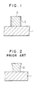
- Fig. 1 is an enlarged view of the conductor film section of the inventive semiconductor device.
- a conductor film 2 made of aluminum alloy including palladium, with a layer of palladium oxide including C being yield on the side wall of the dry-etched conductor film.
- the presence of the layer 3 prevents side etching on the side wall of conductor film during the dry etching process for forming a conductor film pattern.
- Fig. 2 shows, in a sense of model, the over etching of side walls of the conductor film resulting from the dry etching process without the prior heat process offered by this invention.
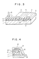
- Fig. 3 is a cross-sectional diagram showing in part the structure of a semiconductor device, e.g., 4 M DRAM or 1 M SRAM, based on one embodiment of this invention.
- a semiconductor device e.g., 4 M DRAM or 1 M SRAM
- indicated by 1 is a semiconductor substrate made of silicon for example
- 4 is an insulator, with contact holes being formed in it, made of SiO2 film or PSG film with a thickness of 0.1-05 ⁇ m for example
- 2 is an Al alloy conductor film made of pure Al or Al including Si added by 0.01-4 weight-% of Pd with a thickness of 0.5-1 ⁇ for LSI in general.
- the Al alloy conductor film 2 contacts with the semiconductor substrate 1 through contact holes.
- the Al alloy conductor film 2 has its exposed surface protected by a passivation film (not shown), e.g., PSG or PIQ film with a thickness of 0.5-2.0 ⁇ m.
- the Al alloy conductor film 2 has a bonding pad, and connection is made by ball bonding using metallic wires 6, e.g., copper wires, aluminum wires or gold wires.
- the bass is created by melting the wire end in the non-oxidative atmosphere and forming it into a ball by utilizing the surface tension.
- the conductor film material After the conductor film material has been formed on the semiconductor substrate 1, it is heat processed so that the compound of aluminum with palladium precipitates in the conductor film. The process is followed by dry etching, by which the intended conductor pattern is completed. During dry etching, conductor patterns are covered by a mask, which is preferably a resist mask for example.
- Fig. 4 shows the resin-molded semiconductor device, in which a semiconductor substrate having a conductor film is placed on a lead frame 7, with the conductor film 2 and lead frame 7 being connected electrically by a metallic wire 6 and, thereafter sealed with resin 8.
- Indicated by 9 in the figure is a passivation film.
- the metallic wire 6 is preferably a copper wire of pure copper or copper including substantially no additive element, or an aluminum wire of pure aluminum or aluminum without additive element.
- the lead frame 7 is preferably made of copper or iron-nickel alloy.
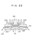
- Fig. 22 shows an application of this invention to an LSI circuit device such as a DRAM with a capacity of 4 MB or more or a SRAM with a capacity of 1 MB or more.
- the device includes a semiconductor substrate 181 in which an LSI circuit is formed, a metallic plate 185, e.g., made of Mo, on which the semiconductor substrate is placed, conductor films 2 fitted on the semiconductor substrate, metallic wires 183 for connecting the conductor films to lead frames 182 electrically, and an electrical insulation cap 184 for providing a hermetical seal for the semiconductor substrate, conductor films and metallic wires.
- the conductor film 2 is formed in such a manner as described in connection with the preceding embodiment.
- the conductor film has its side wall cut in a rectangular or virtually rectangular profile, with a protective film including the oxide of Pd included in the conductor film material and C being formed on the side wall surface.
- the metallic plate which supports the semiconductor substrate is made up of a molybdenum plate 185 and a gold-plated copper stand 186.
- the LSI 181 is fixed on the Mo plate by gold plating.
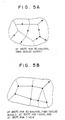
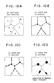
- Fig. 5A shows the matrix structure of the conductor film made of Al - 1 weight-% Si - 0.5 weight-% Pd alloy resulting from the heat process at 450°C for 30 minutes.
- Fig. 5B shows the matrix structure of the same conductor film resulting from the second heat processes at 300°C for 1 hour and at 350°C for 1 hour following the above-mentioned heat process. The second heat process may be conducted in divided cycles as in this case.
- precipitations exist on usual grain boundaries, whereas in Fig. 5B, they exist concentrically on grain boundary triple points. Detailed examination of precipitation in both structures revealed that grain boundary precipitations are 90% or more of all in the structure of Fig. 5A, while those on grain boundary are less than 10% in the structure of Fig. 5B.
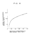
- Fig. 6 shows the relation between the proportion of precipitations located on grain boundary triple points and the mean time t50 until the conductor is broken by electromigration when a current of 2 x 10⁶ A/cm2 is applied to stripes of the same lot.
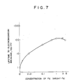
- Fig. 7 shows the relation between the mean life time t50 and the quantity of Pd addition for the conductor in which 30% of precipitations are located on grain boundary triple points. As indicated on the graph, the addition of Pd by 0.01 weight-% or more is effective. It will be appreciated from Figs. 6 and 7 that a proper amount of additive Pd is 0.01-3 weight-%, and an increased proportion of precipitations on grain boundary triple points further enhances the resistance against electromigration.
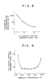
- Fig. 8 shows the relation between the dispersion angle of dominant direction of Al (111) grains and the mean time to breakage for a conductor film of Al - 0.5 weight-% Pd - 1 weight-% Si alloy after it has been annealed and then subjected to another heat process (precipitation heat process).
- Aluminum grains are generally polarized on the most stable plane 111, while each grain has its ⁇ 111> direction deviated slightly from one another. This deviation is measured using the X-rays, and its mean value is defined to be the dispersion angle.
- a great dispersion angle signifies a great disruption of crystal grain boundaries.
- Fig. 9 shows the relation between the dispersion angle and the annealing temperature
- Fig. 10 shows the relation between the precipitation heat process and the matrix structure annealed at 400°C for 30 minutes.
- Fig. 9 implies that a too low annealing temperature does not allow re-arrangement of grains, while a too high annealing temperature causes re-crystallization and the dispersion angle does not become smaller. Accordingly, the annealing condition of 200-450°C for 3-180 minutes enhances the anti-migration property.
- Fig. 9 implies that a too low annealing temperature does not allow re-arrangement of grains, while a too high annealing temperature causes re-crystallization and the dispersion angle does not become smaller. Accordingly, the annealing condition of 200-450°C for 3-180 minutes enhances the anti-migration property.
- Fig. 9 implies that a too low annealing temperature does not allow re-arrangement
- a layer of palladium oxide is formed on the side wall of the film as shown in Fig. 1.
- This palladium oxide includes C as mentioned previously, and the quantity of C included can be controlled by adjusting the etching conditions such as atomospheric gas compositions, etching power and/or etching time interval.
- Fig. 21 shows the relation between the quantity of C and the corrosion current at the natural corrosion voltage in the 100 ppm aqueous solution of Cl ion indicative of the film corrosive property. The figure indicates that the corrosion current decreases to 1/100 as the quantity of C increases to 0.01% or more.
- Table 1 shows the reduction of pattern dimension demonstrated by conductor films of 0.5 ⁇ m in thickness formed of several conductor film materials by sputtering and, after the heat process, dry-etched to a line width of 1 ⁇ m.
- the conductor film of the Al - 0.5 wt% (weight-%) Pd - 1 wt% Si alloy attains a minimal reduction of dimension.
- Fig. 11 is a brief cross-sectional view of the semiconductor device according to one embodiment of this invention.
- Palladium silicide 25 is formed partly between an Al alloy conductor film 2 and a Si diffusion layer 24.
- Indicated by 22 is a passivation film, and 23 is a heat-oxidized SiO2 film.
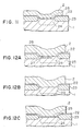
- Figs. 12A-12C show, as an example, the fabricating process of the inventive semiconductor device.
- a conventional conductor film of Al - 1 weight-% Si - 1 weight-% Pd alloy is formed on a semiconductor substrate 1 by sputtering, and a conductor pattern is formed through the photo-etching process, as shown in Fig. 12A.
- lattice defects 27 created by sputtering for the conductor film material are left inside the diffusion layer 24 and an oxide film 28 is left on the surface of the diffusion layer 24.
- annealing is conducted at 400°C for 30 minutes. This process recovers the defects 27 of sputtering to form a good ohmic contact, as shown in Fig. 12B.
- a natural oxide film 28 left on the surface of the Al alloy conductor film at its deposition is reduced by Al, and the semiconductor substrate has a clean Si surface. After that, another heat process is conducted at 200°C for 2 hours. Consequently, Pd in the Al alloy concentrates on the Si interface, where it reacts with Si to yield silicide, as shown in Fig. 12C.
- Fig. 13 shows the result of X-ray photoelectron spectroscopy (XPS) on the Si interface after the overlying Al alloy film has been etched off.
- the Al alloy and Al metallic compound are removed by etching, while precipitations to other interfaces remain and they are detected by the XPS analysis.
- Pd, Si, O and C detected, O and C are derived from the contamination on the Si surface sustained in the etching process.
- a further detailed examination on the detected Pd3d5/2 peak revealed that the Pd forms Pd2Si as shown in Fig. 14.
- Table 2 shows the proportion of area of Pd2Si which covers the Si interface, with the heat process of 200°C being shortened to 60 minutes and 30 minutes, evaluated from the XPS spectrum intensity.
- Table 2 Heat Condition Relative value of Pd3d5/2 peak area (The value is 1 when annealing at 200°C, 2 hours)
- Proportion of Pd2Si interface (%) 200°C, 30 minutes 0.2 20 1 hour 0.5 50 2 hours 1 100 3 hours 1.0 100 4 hours 1.05 100
- the 30-minute re-heating does not make 80% of Si interface to become silicide, and the following annealing at 450°C for 60 minutes does not cause Si precipitations to grow.
- the contact resistance increased by only 77% before and after the annealing at 450°C for 60 minutes. This resistance increase is half or less the case of the conventional technique using Al - 1 weight-% Si alloy, presenting the effectiveness of this invention.
- the silicide formation is effective even if it does not cover the entire Si interface.
- Fig. 15 shows the XPS spectrum on the Si interface after the heat process which is conducted in this case by lowering the re-heating temperature of 200°C to 150°C for a duration of 2 hours.
- precipitations of pure Pd occur on the interface besides Pd2Si.
- a successive annealing at 450°C for 60 minutes causes the precipitations of pure Pd to be absorbed back into the Al alloy film, resulting in a weakened suppression effect against Si precipitation.
- a sufficient amount of Pd2Si is formed on the interface to effectively suppress Si precipitation, as shown in Table 3.
- Table 3 Process Condition Contact resistance before 450°C, 60 min.
- annealing ra (1.2 ⁇ m ⁇ CONT) Contact resistance after 450°C, 60 min. annealing rb Increase in contact resistance (rb-ra)/ra (%) Proportion if Si precipitations on contact interface after 450°C, 60 min. annealing (%) Al-Pd-Si 200°C 30 min 22 ⁇ 39 ⁇ 77 10 1 hour 24 35 45 7 2 hours 26 30 15 ⁇ 5 150°C 2 hours 24 40 66 15 Al-1% Si 400°C, 30 min. Ohnic formation only 20 60 200 >30
- silicide needs to be formed as uniform as possible at a low temperature.
- Table 4 lists a variety of silicide which can be formed at relatively low temperatures.
- Table 4 Silicide Forming temperature (°C) Mg2Si ⁇ 200 Co2Si 350 - 500 CoSi 400 - 500 Ni3Si ⁇ 200 Ni5Si2 ⁇ 200 Ni2Si 200 - 350 NiSi 350 - 750 Pd2Si ⁇ 100 Pt2Si 200 - 500 PtSi ⁇ 300
- Mg Besides Pd which forms silicide at the lowest temperature, another element which forms only one type of silicide at a low temperature is Mg, but Mg easily forms solid solution with Al when added to it and does not emerge on the Si interface.
- the conductor film material is desirably deposited by chemical vapor deposition (CVD), electron beam (EB) evapolative deposition, or sputtering.
- CVD chemical vapor deposition
- EB electron beam
- sputtering use of a target, with the concentration distribution of additive element being controlled within ⁇ 0.05%, is recommended to produce a uniform Al conductor film with outstanding characteristics.
- the conductor film material based on aluminum or aluminum including silicon by less than 3 weight-% includes less than 5 weight-% of palladium or platinum as additive element and further includes at least one of lithium, beryllium, magnesium, manganese, iron, cobalt, nickel, copper, lanthanum, cerium, chrome, hafnium, zirconium, cadmium, titanium, tungsten, vanadium, tantalum, and niobium by less than 5 weight-% as additional additive element.
- the above material is deposited on a semiconductor substrate by sputtering, and the anneal process at 400-500°C for 10 minutes or longer is conducted as a first-stage heat process thereby to form a solid solution of the additive elements on the Al matrix. Then the whole substrate is cooled quickly at a rate of 10°C/sec so that the Al matrix becomes a super-saturated solid solution of the additive elements. Next, the precipitation heat process is conducted at 350°C or lower for 20-60 minutes so that the super-saturated solid solution makes precipitates as fine compound, and thereafter another heat process is conducted at the same annealing temperature for 10 minutes or less so that the additive elements are made solid solution again in the Al matrix.
- the Al conductor film formed as described above initially includes precipitations of metallic compound between palladium or platinum and aluminum, and, as the time passes on, the electron current flowing in the conductor causes other additive element in solid solution to precipitate successively. Consequently, a fine conductor film with a line width of 2 ⁇ m or less has its resistances against electromigration and stress migration, respectively, enhanced significantly.
- Fig. 16 compares the life time to breakage resulting from electromigration of the conductor films formed by the inventive method described above and those formed by the conventional method, the test being based on the current conduction at a high temperature.
- three rows in the upper section are the test results for the conductor films formed by the conventional method.
- the life time of conductor evaluated here is defined to be the time length at which a half of the test samples are broken.
- the inventive Al alloy conductors are superior in life time to the conventional conductors.
- Fig. 17A shows the grain boundary structure of the Al alloy conductor film based on the foregoing inventive heat process
- Figs. 17B, 17C and 17D show the grain boundary structure of the Al-Si, Al-Pd-Si and Al-Pd-Cu-Si conductor materials, respectively, based on the conventional heat process at 450°C for 1 hour.
- the Al alloy film structures were observed after the application of current at a high current density of 8 x 10⁶ A/cm2 for 3 hours.
- both coarse precipitations and fine precipitations emerge on grain boundaries, standing for the occurrence of fine precipitation reaction.
- the other three samples exhibit over-growing precipitations, and therefore the suppression of the diffusion through grain boundaries by dislocation pinning effect is lost.
- Fig. 18 shows the pattern dimension accuracy after dry etching using chlorine-based gas for the Al alloy conductor based on the embodiment of this invention and the conventional Al plus Si conductor.
- the property of formation based on the embodiment is superior particularly for semiconductor devices, e.g., 4M DRAM and 1M SRAM, where the pattern dimension is 1 ⁇ m or smaller.
- Fig. 19 shows the result of examination on the cumulative fault rate attributable to stress migration for the conventional Al-Si conductor and Al-Pd-Si conductor and the Al-Pd-Mg-Si conductor based on the embodiment of this invention.
- the addition of Mg enhances the stress migration resistance significantly.
- the same effectiveness is achieved by the addition of at least one of the aforementioned additive elements besides Mg.
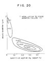
- Fig. 20 shows the change in the life time of conductor to stress migration failure when the Al-Pd-Si conductor film added by Mg is heat processed as described above so that grains are made smaller than the conductor width (0.8 ⁇ m). As shown clearly in Fig. 20, samples with the addition of more Mg and having smaller grains are higher in stability, and samples having grain diameters larger than the conductor width are shorter in life to stress migration failure.
- a conceivable reason is that the stress migration breakage is caused by the grain boundary diffusion of Al atoms ascribed to the tensional stress, and, in case of comparable dimensions of the conductor and Al grains, grain boundary diffusion occurring at one position has an increased possibility of being destined to failure.
- a finer grain dimension is also accomplished by use of the aforementioned additive elements besides Mg.
- the reason for the grain diameter to become smaller than 1 ⁇ m is conceivably re-crystallization of Al matrix which takes place in, among the inventive heat process, the short-term re-heating at the annealing temperature following the precipitation process.
Landscapes
- Internal Circuitry In Semiconductor Integrated Circuit Devices (AREA)
Applications Claiming Priority (4)
| Application Number | Priority Date | Filing Date | Title |
|---|---|---|---|
| JP834988 | 1988-01-20 | ||
| JP8349/88 | 1988-01-20 | ||
| JP59451/88 | 1988-03-15 | ||
| JP63059451A JPH01233737A (ja) | 1988-03-15 | 1988-03-15 | 集積回路装置及びその製造方法並びに該装置における配線膜を製造するためのターゲット |
Publications (3)
| Publication Number | Publication Date |
|---|---|
| EP0326018A2 true EP0326018A2 (fr) | 1989-08-02 |
| EP0326018A3 EP0326018A3 (fr) | 1991-04-17 |
| EP0326018B1 EP0326018B1 (fr) | 1997-11-19 |
Family
ID=26342845
Family Applications (1)
| Application Number | Title | Priority Date | Filing Date |
|---|---|---|---|
| EP89100865A Expired - Lifetime EP0326018B1 (fr) | 1988-01-20 | 1989-01-19 | Dispositif semiconducteur et procédé de fabrication |
Country Status (4)
| Country | Link |
|---|---|
| US (1) | US5019891A (fr) |
| EP (1) | EP0326018B1 (fr) |
| KR (1) | KR0132786B1 (fr) |
| DE (1) | DE68928448T2 (fr) |
Cited By (8)
| Publication number | Priority date | Publication date | Assignee | Title |
|---|---|---|---|---|
| EP0435009A3 (en) * | 1989-12-27 | 1991-09-25 | Tanaka Denshi Kogyo Kabushiki Kaisha | Semiconductor package connecting method, semiconductor package connecting wires and semiconductor devices |
| DE4303401A1 (en) * | 1992-02-17 | 1993-08-19 | Mitsubishi Electric Corp | Semiconductor device e.g. DRAM mfr. - involves hole-free passive oxide film prodn. on bonding pad |
| DE4337209A1 (de) * | 1993-10-30 | 1995-05-04 | Abb Management Ag | Abschaltbarer Thyristor |
| EP0725439A3 (fr) * | 1992-08-27 | 1996-10-30 | Toshiba Kk | Pièce électronique avec interconnexions métalliques et procédé pour sa fabrication |
| US5709958A (en) * | 1992-08-27 | 1998-01-20 | Kabushiki Kaisha Toshiba | Electronic parts |
| US5830786A (en) * | 1993-02-22 | 1998-11-03 | Semiconductor Energy Laboratory Co., Ltd. | Process for fabricating electronic circuits with anodically oxidized scandium doped aluminum wiring |
| US6001461A (en) * | 1992-08-27 | 1999-12-14 | Kabushiki Kaisha Toshiba | Electronic parts and manufacturing method thereof |
| US6075278A (en) * | 1997-04-24 | 2000-06-13 | Micron Technology, Inc. | Aluminum based alloy bridge structure and method of forming same |
Families Citing this family (21)
| Publication number | Priority date | Publication date | Assignee | Title |
|---|---|---|---|---|
| EP0256557B1 (fr) * | 1986-08-19 | 1993-01-07 | Fujitsu Limited | Dispositif semi-conducteur comprenant une couche de métallisation à film mince et son procédé de fabrication |
| US5243221A (en) * | 1989-10-25 | 1993-09-07 | At&T Bell Laboratories | Aluminum metallization doped with iron and copper to prevent electromigration |
| KR940008936B1 (ko) * | 1990-02-15 | 1994-09-28 | 가부시끼가이샤 도시바 | 고순도 금속재와 그 성질을 이용한 반도체 장치 및 그 제조방법 |
| US5173354A (en) * | 1990-12-13 | 1992-12-22 | Cornell Research Foundation, Inc. | Non-beading, thin-film, metal-coated ceramic substrate |
| US5500301A (en) * | 1991-03-07 | 1996-03-19 | Kabushiki Kaisha Kobe Seiko Sho | A1 alloy films and melting A1 alloy sputtering targets for depositing A1 alloy films |
| TW232079B (fr) * | 1992-03-17 | 1994-10-11 | Wisconsin Alumni Res Found | |
| US5448113A (en) * | 1993-03-08 | 1995-09-05 | Ricoh Company, Ltd. | Micro metal-wiring structure having stress induced migration resistance |
| JPH0737706A (ja) * | 1993-07-19 | 1995-02-07 | Murata Mfg Co Ltd | 半導体セラミック素子 |
| US5434104A (en) * | 1994-03-02 | 1995-07-18 | Vlsi Technology, Inc. | Method of using corrosion prohibiters in aluminum alloy films |
| US5711858A (en) * | 1994-04-12 | 1998-01-27 | International Business Machines Corporation | Process for depositing a conductive thin film upon an integrated circuit substrate |
| KR960028689A (ko) * | 1994-12-26 | 1996-07-22 | 이형도 | 센서용 히터전극 및 이를 사용한 세라믹 히터 |
| KR100231838B1 (ko) * | 1997-05-20 | 1999-12-01 | 유무성 | 집적회로용 리드프레임 및 그 제조방법 |
| US6339026B1 (en) | 1998-04-24 | 2002-01-15 | Micron Technology, Inc. | Semiconductor processing methods of polishing aluminum-comprising layers |
| US6522010B2 (en) | 1998-06-30 | 2003-02-18 | Micron Technology, Inc. | Semiconductor constructions comprising aluminum-containing layers |
| JP2000150652A (ja) * | 1998-09-03 | 2000-05-30 | Seiko Epson Corp | 半導体装置およびその製造方法 |
| JP3533968B2 (ja) | 1998-12-22 | 2004-06-07 | セイコーエプソン株式会社 | 半導体装置の製造方法 |
| JP2003089864A (ja) * | 2001-09-18 | 2003-03-28 | Mitsui Mining & Smelting Co Ltd | アルミニウム合金薄膜及びその薄膜を有する配線回路並びにその薄膜を形成するターゲット材 |
| US6955980B2 (en) * | 2002-08-30 | 2005-10-18 | Texas Instruments Incorporated | Reducing the migration of grain boundaries |
| JP2005086118A (ja) * | 2003-09-11 | 2005-03-31 | Renesas Technology Corp | 半導体装置 |
| US7656045B2 (en) * | 2006-02-23 | 2010-02-02 | Freescale Semiconductor, Inc. | Cap layer for an aluminum copper bond pad |
| JP5524905B2 (ja) * | 2011-05-17 | 2014-06-18 | 株式会社神戸製鋼所 | パワー半導体素子用Al合金膜 |
Family Cites Families (9)
| Publication number | Priority date | Publication date | Assignee | Title |
|---|---|---|---|---|
| NL87258C (fr) * | 1969-01-15 | |||
| US4065781A (en) * | 1974-06-21 | 1977-12-27 | Westinghouse Electric Corporation | Insulated-gate thin film transistor with low leakage current |
| US4127424A (en) * | 1976-12-06 | 1978-11-28 | Ses, Incorporated | Photovoltaic cell array |
| JPS6026640A (ja) * | 1983-07-25 | 1985-02-09 | Hitachi Ltd | 耐食性アルミニウム電子材料 |
| JPS61144847A (ja) * | 1984-12-19 | 1986-07-02 | Hitachi Ltd | 半導体装置およびその製造法 |
| US4843453A (en) * | 1985-05-10 | 1989-06-27 | Texas Instruments Incorporated | Metal contacts and interconnections for VLSI devices |
| JPS6379950A (ja) * | 1986-09-22 | 1988-04-09 | Hitachi Ltd | 耐食性保護膜を有する物品及びその製造方法 |
| US4800419A (en) * | 1987-01-28 | 1989-01-24 | Lsi Logic Corporation | Support assembly for integrated circuits |
| US4827326A (en) * | 1987-11-02 | 1989-05-02 | Motorola, Inc. | Integrated circuit having polyimide/metal passivation layer and method of manufacture using metal lift-off |
-
1989
- 1989-01-12 US US07/296,003 patent/US5019891A/en not_active Expired - Lifetime
- 1989-01-19 DE DE68928448T patent/DE68928448T2/de not_active Expired - Fee Related
- 1989-01-19 EP EP89100865A patent/EP0326018B1/fr not_active Expired - Lifetime
- 1989-01-19 KR KR1019890000525A patent/KR0132786B1/ko not_active Expired - Fee Related
Cited By (14)
| Publication number | Priority date | Publication date | Assignee | Title |
|---|---|---|---|---|
| US5550407A (en) * | 1989-12-27 | 1996-08-27 | Tanaka Denshi Kogyo Kabushiki Kaisha | Semiconductor device having an aluminum alloy wiring line |
| EP0435009A3 (en) * | 1989-12-27 | 1991-09-25 | Tanaka Denshi Kogyo Kabushiki Kaisha | Semiconductor package connecting method, semiconductor package connecting wires and semiconductor devices |
| US5366692A (en) * | 1989-12-27 | 1994-11-22 | Tanaka Denshi Kogyo Kabushiki Kaisha | Alloy connecting materials for semiconductors |
| DE4303401C2 (de) * | 1992-02-17 | 1998-06-04 | Mitsubishi Electric Corp | Verfahren zum Herstellen einer Halbleitervorrichtung |
| US5565378A (en) * | 1992-02-17 | 1996-10-15 | Mitsubishi Denki Kabushiki Kaisha | Process of passivating a semiconductor device bonding pad by immersion in O2 or O3 solution |
| DE4303401A1 (en) * | 1992-02-17 | 1993-08-19 | Mitsubishi Electric Corp | Semiconductor device e.g. DRAM mfr. - involves hole-free passive oxide film prodn. on bonding pad |
| EP0725439A3 (fr) * | 1992-08-27 | 1996-10-30 | Toshiba Kk | Pièce électronique avec interconnexions métalliques et procédé pour sa fabrication |
| US5709958A (en) * | 1992-08-27 | 1998-01-20 | Kabushiki Kaisha Toshiba | Electronic parts |
| US6001461A (en) * | 1992-08-27 | 1999-12-14 | Kabushiki Kaisha Toshiba | Electronic parts and manufacturing method thereof |
| US5830786A (en) * | 1993-02-22 | 1998-11-03 | Semiconductor Energy Laboratory Co., Ltd. | Process for fabricating electronic circuits with anodically oxidized scandium doped aluminum wiring |
| US5491351A (en) * | 1993-10-30 | 1996-02-13 | Abb Management Ag | Gate turn-off thyristor |
| DE4337209A1 (de) * | 1993-10-30 | 1995-05-04 | Abb Management Ag | Abschaltbarer Thyristor |
| US6075278A (en) * | 1997-04-24 | 2000-06-13 | Micron Technology, Inc. | Aluminum based alloy bridge structure and method of forming same |
| US6624519B1 (en) | 1997-04-24 | 2003-09-23 | Micron Technology, Inc. | Aluminum based alloy bridge structure and method of forming same |
Also Published As
| Publication number | Publication date |
|---|---|
| US5019891A (en) | 1991-05-28 |
| KR0132786B1 (ko) | 1998-04-16 |
| DE68928448T2 (de) | 1998-03-12 |
| KR890012377A (ko) | 1989-08-26 |
| EP0326018A3 (fr) | 1991-04-17 |
| EP0326018B1 (fr) | 1997-11-19 |
| DE68928448D1 (de) | 1998-01-02 |
Similar Documents
| Publication | Publication Date | Title |
|---|---|---|
| EP0326018B1 (fr) | Dispositif semiconducteur et procédé de fabrication | |
| US6642623B2 (en) | Multi-layered copper bond pad for an integrated circuit | |
| US5712194A (en) | Semiconductor device including interlayer dielectric film layers and conductive film layers | |
| US7081680B2 (en) | Self-aligned corrosion stop for copper C4 and wirebond | |
| EP0030633A1 (fr) | Conducteurs en nickel-or-nickel pour des composants solides | |
| KR100528743B1 (ko) | 집적 회로 구조체 및 집적 회로 구조체를 마련하는 공정 | |
| EP0725439B1 (fr) | Pièce électronique avec interconnexions métalliques et procédé pour sa fabrication | |
| US5051812A (en) | Semiconductor device and method for manufacturing the same | |
| US6435398B2 (en) | Method for chemically reworking metal layers on integrated circuit bond pads | |
| US4022931A (en) | Process for making semiconductor device | |
| JP2810076B2 (ja) | 半導体装置およびその製造方法 | |
| EP0082012B1 (fr) | Electrode à multicouches d'un dispositif semi-conducteur | |
| JPH06236878A (ja) | 金属配線 | |
| JPH01233737A (ja) | 集積回路装置及びその製造方法並びに該装置における配線膜を製造するためのターゲット | |
| US5565380A (en) | Semiconductor device and process for production thereof | |
| JP3033803B2 (ja) | 半導体装置の製造方法 | |
| JPH04192332A (ja) | 薄膜配線の製造方法並びに薄膜配線及び半導体装置 | |
| US4902582A (en) | Aluminum metallized layer formed on silicon wafer | |
| US6960306B2 (en) | Low Cu percentages for reducing shorts in AlCu lines | |
| JP3356319B2 (ja) | 半導体装置及びその製造方法 | |
| JPH06208999A (ja) | 半導体装置の製造方法 | |
| JPH07111970B2 (ja) | 低い割合のバナジウムを含むアルミニウムの相互接続層を有した半導体装置及び方法 | |
| JPH06310608A (ja) | 半導体装置の製造方法 | |
| JPH05102156A (ja) | 半導体装置 | |
| JPH02232927A (ja) | 電子部品 |
Legal Events
| Date | Code | Title | Description |
|---|---|---|---|
| PUAI | Public reference made under article 153(3) epc to a published international application that has entered the european phase |
Free format text: ORIGINAL CODE: 0009012 |
|
| AK | Designated contracting states |
Kind code of ref document: A2 Designated state(s): DE FR GB IT |
|
| 17P | Request for examination filed |
Effective date: 19901119 |
|
| PUAL | Search report despatched |
Free format text: ORIGINAL CODE: 0009013 |
|
| AK | Designated contracting states |
Kind code of ref document: A3 Designated state(s): DE FR GB IT |
|
| 17Q | First examination report despatched |
Effective date: 19931014 |
|
| GRAG | Despatch of communication of intention to grant |
Free format text: ORIGINAL CODE: EPIDOS AGRA |
|
| GRAH | Despatch of communication of intention to grant a patent |
Free format text: ORIGINAL CODE: EPIDOS IGRA |
|
| GRAH | Despatch of communication of intention to grant a patent |
Free format text: ORIGINAL CODE: EPIDOS IGRA |
|
| GRAA | (expected) grant |
Free format text: ORIGINAL CODE: 0009210 |
|
| AK | Designated contracting states |
Kind code of ref document: B1 Designated state(s): DE FR GB |
|
| REF | Corresponds to: |
Ref document number: 68928448 Country of ref document: DE Date of ref document: 19980102 |
|
| ET | Fr: translation filed | ||
| PLBE | No opposition filed within time limit |
Free format text: ORIGINAL CODE: 0009261 |
|
| STAA | Information on the status of an ep patent application or granted ep patent |
Free format text: STATUS: NO OPPOSITION FILED WITHIN TIME LIMIT |
|
| 26N | No opposition filed | ||
| PGFP | Annual fee paid to national office [announced via postgrant information from national office to epo] |
Ref country code: FR Payment date: 20001218 Year of fee payment: 13 |
|
| PGFP | Annual fee paid to national office [announced via postgrant information from national office to epo] |
Ref country code: GB Payment date: 20001228 Year of fee payment: 13 |
|
| PGFP | Annual fee paid to national office [announced via postgrant information from national office to epo] |
Ref country code: DE Payment date: 20010330 Year of fee payment: 13 |
|
| REG | Reference to a national code |
Ref country code: GB Ref legal event code: IF02 |
|
| PG25 | Lapsed in a contracting state [announced via postgrant information from national office to epo] |
Ref country code: GB Free format text: LAPSE BECAUSE OF NON-PAYMENT OF DUE FEES Effective date: 20020119 |
|
| PG25 | Lapsed in a contracting state [announced via postgrant information from national office to epo] |
Ref country code: DE Free format text: LAPSE BECAUSE OF NON-PAYMENT OF DUE FEES Effective date: 20020801 |
|
| GBPC | Gb: european patent ceased through non-payment of renewal fee |
Effective date: 20020119 |
|
| PG25 | Lapsed in a contracting state [announced via postgrant information from national office to epo] |
Ref country code: FR Free format text: LAPSE BECAUSE OF NON-PAYMENT OF DUE FEES Effective date: 20020930 |
|
| REG | Reference to a national code |
Ref country code: FR Ref legal event code: ST |