EP0326064B1 - Circuit d'alimentation pour alimenter au moins une charge avec une source de courant continu - Google Patents
Circuit d'alimentation pour alimenter au moins une charge avec une source de courant continu Download PDFInfo
- Publication number
- EP0326064B1 EP0326064B1 EP89101132A EP89101132A EP0326064B1 EP 0326064 B1 EP0326064 B1 EP 0326064B1 EP 89101132 A EP89101132 A EP 89101132A EP 89101132 A EP89101132 A EP 89101132A EP 0326064 B1 EP0326064 B1 EP 0326064B1
- Authority
- EP
- European Patent Office
- Prior art keywords
- voltage
- input
- supply circuit
- output
- switch
- Prior art date
- Legal status (The legal status is an assumption and is not a legal conclusion. Google has not performed a legal analysis and makes no representation as to the accuracy of the status listed.)
- Expired - Lifetime
Links
- 238000004804 winding Methods 0.000 claims description 28
- 239000003990 capacitor Substances 0.000 claims description 14
- 238000005516 engineering process Methods 0.000 claims description 3
- 230000000903 blocking effect Effects 0.000 description 7
- 230000033228 biological regulation Effects 0.000 description 6
- 230000001105 regulatory effect Effects 0.000 description 5
- 238000004891 communication Methods 0.000 description 2
- 230000007423 decrease Effects 0.000 description 2
- 101100537098 Mus musculus Alyref gene Proteins 0.000 description 1
- 101100269674 Mus musculus Alyref2 gene Proteins 0.000 description 1
- 101150095908 apex1 gene Proteins 0.000 description 1
- 230000015572 biosynthetic process Effects 0.000 description 1
- 238000010276 construction Methods 0.000 description 1
- 230000000694 effects Effects 0.000 description 1
- 239000000835 fiber Substances 0.000 description 1
- 230000005669 field effect Effects 0.000 description 1
- 239000004065 semiconductor Substances 0.000 description 1
- 238000000926 separation method Methods 0.000 description 1
- 238000011144 upstream manufacturing Methods 0.000 description 1
- 238000003079 width control Methods 0.000 description 1
Images
Classifications
-
- H—ELECTRICITY
- H02—GENERATION; CONVERSION OR DISTRIBUTION OF ELECTRIC POWER
- H02M—APPARATUS FOR CONVERSION BETWEEN AC AND AC, BETWEEN AC AND DC, OR BETWEEN DC AND DC, AND FOR USE WITH MAINS OR SIMILAR POWER SUPPLY SYSTEMS; CONVERSION OF DC OR AC INPUT POWER INTO SURGE OUTPUT POWER; CONTROL OR REGULATION THEREOF
- H02M3/00—Conversion of DC power input into DC power output
- H02M3/22—Conversion of DC power input into DC power output with intermediate conversion into AC
- H02M3/24—Conversion of DC power input into DC power output with intermediate conversion into AC by static converters
- H02M3/28—Conversion of DC power input into DC power output with intermediate conversion into AC by static converters using discharge tubes with control electrode or semiconductor devices with control electrode to produce the intermediate AC
- H02M3/325—Conversion of DC power input into DC power output with intermediate conversion into AC by static converters using discharge tubes with control electrode or semiconductor devices with control electrode to produce the intermediate AC using devices of a triode or a transistor type requiring continuous application of a control signal
- H02M3/335—Conversion of DC power input into DC power output with intermediate conversion into AC by static converters using discharge tubes with control electrode or semiconductor devices with control electrode to produce the intermediate AC using devices of a triode or a transistor type requiring continuous application of a control signal using semiconductor devices only
- H02M3/33507—Conversion of DC power input into DC power output with intermediate conversion into AC by static converters using discharge tubes with control electrode or semiconductor devices with control electrode to produce the intermediate AC using devices of a triode or a transistor type requiring continuous application of a control signal using semiconductor devices only with automatic control of the output voltage or current, e.g. flyback converters
Definitions
- the invention relates to a feed circuit for feeding at least one consumer from an impressed direct current, as specified in the preamble of patent claim 1.
- Such a supply circuit is already known from EP-A1-0 170 932.
- a voltage converter is arranged in a chain with a switching regulator.
- a current sensor for the input current is provided at the input of the voltage converter.
- the voltage converter is controlled by means of the current sensor and a control circuit connected to the current sensor in such a way that it outputs a reduced output voltage or output power at input currents above a predetermined limit value. In this way it is achieved that the supply circuit is largely insensitive to overload conditions.
- the known supply circuit is able to automatically switch to the normal operating state following an overload condition.
- the object of the invention is to provide a supply circuit for supplying at least one consumer with a direct voltage obtained from an impressed direct current in such a way that - apart from any regulators or the like which may be provided - it is designed in one stage and thereby guarantees a power limitation of the output circuit or the output circuits.
- the feed circuit for solving this problem is designed in the manner specified in the characterizing part of patent claim 1.
- the supply circuit generates at least one constant, electrically isolated output voltage and, in particular with a low-impedance load, outputs constant voltages at output voltages which are less than or equal to the nominal voltage.
- a power limitation is expediently provided for the output circuit or for the output circuits.
- the input voltage is limited to the value which corresponds to the maximum power, this advantageously results in a control of the power consumption to a constant value, so that at high load or at low Load resistances over the efficiency result in an almost constant output power.
- the EMF is regulated to a constant value.
- the measures according to claim 4 can prove expedient when limiting the input voltage.
- the further embodiment according to claim 5 has the advantage that only a single control comparator is required to control the EMF and to limit the input voltage.
- the measures according to claim 6 enable a particularly simple construction of the transformer.
- a limitation of the output current can be provided instead of the limitation of the power.
- the output power decreases as the load resistance decreases, so that the output power has a predetermined upper limit cannot exceed.
- the potential separation between the input and output power circuit is ensured in particular by the measures according to claim 8.
- the feed circuit is particularly suitable for use in a device for remote feeding of intermediate points in devices of electrical or electro-optical communication technology.
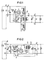
- the feed circuit shown in FIG. 1 for feeding the consumer V generates the impressed output voltage U2 from the impressed current i0.
- the supply circuit can serve, in particular in remote supply devices with direct current series supply, to supply one or more consumers with voltage in each case at remote-supplied intermediate points.
- the input a1, b1 is in series with other similar feed circuits, not shown, in a remote feed circuit into which the constant current source Q feeds the contact current i0.
- the supply circuit is a constant-current blocking converter educated.
- a series circuit comprising the primary winding 61 of the storage transformer 6 and the controllable switch 5 is connected to the input a1, b1 of the supply circuit.
- the controllable switch 5 is therefore in a current branch arranged parallel to the input a1, b1 of the feed circuit.
- the capacitor 21 is connected to the input a1, b1 of the supply circuit.
- the series circuit comprising the diode 73 and the capacitor 23 is connected to the secondary winding 62 of the transformer 6.
- the diode 73 is polarized so that it is conductive when the switch 5 is off and blocked when the switch 5 is on.
- Output a2, b2 of the supply circuit, to which consumer V is connected, is connected in parallel with capacitor 23.
- the blocking converter can have further secondary circuits for supplying further loads, preferably those which are constructed like the secondary circuit consisting of the secondary winding 62, the diode 73 and the capacitor 23.
- the blocking converter is provided with a control arrangement, with the aid of which the open circuit voltage or the EMF is regulated to a constant value.
- the auxiliary voltage U H occurring at the capacitor 22 serves as a measure of the open circuit voltage.
- This auxiliary voltage U H is supplied as a supply voltage to the operating voltage inputs of the control comparator 31 and the pulse width modulator 4 and is supplied to the control comparator 31 as an actual value via the voltage divider consisting of the resistors 19 and 20.
- the control comparator 31 controls the pulse width modulator 4.
- the switch 5 which can be formed in particular by a semiconductor switch or power field effect transistor, is alternately controlled by the sequence of control pulses in the conductive and in the blocked state.
- the capacitor 22 is connected to the winding 63 of the transformer 6 via the diode 71.
- the diode 71 is polarized so that it is blocked when the switch 5 is conductive and is conductive when the switch 5 is blocked.
- the voltage U H is therefore a measure of the open circuit voltage U0 or EMK, which in turn is decisive for the output voltage U2 from which the consumer V is fed.
- the control comparator 31 is an operational amplifier which is connected directly to the input terminal b1 with its reference potential input and to the reference voltage U Ref with its positive input.
- a connection of the capacitor 22 is also connected to the input connection b1, ie to the reference potential.
- the other connection of the capacitor 22 is connected via a voltage divider 19, 20 to the negative input of the control comparator 31 serving as the actual value input.
- the pulse width modulator 4 is in turn controlled by the control comparator 31 so that the pulse-pause ratio of the control pulse train is changed as a function of the control deviation.
- the pulse width modulator 4 is controlled by the control comparator 31 in such a way that in the control range of the supply circuit the relative switch-on time of the switch 5 becomes increasingly greater with larger auxiliary voltages U H and thus also with larger output voltages U2.
- the duration of the control pulses is varied at a fixed pulse repetition frequency.
- the pulse width modulator 4 is controlled as a function of the input voltage U1, in such a way that the relative duty cycle of the controllable switch 5 becomes increasingly greater with larger input voltages U1.
- the voltage U1 ′ induced on the winding 64 is greater than the open circuit voltage U0 and instead of the open circuit voltage U0, one of the input voltage U1 of the supply circuit takes over proportional voltage U1 ', which is supplied by the winding 64 of the transformer 6, the role of the actual value.
- auxiliary voltage U H coupled to the output voltage U2 and the voltage U1 'coupled to the input voltage U1' are alternatively effective in that the capacitor 22 has two current branches connected in parallel.
- Diode 71 is arranged in series with winding 63 in a first current branch, and diode 72 is arranged in series with winding 64 in a second current branch. These two current branches are connected in parallel. With this parallel connection, the cathodes, i.e. electrodes of the same name of the diodes 71 are connected to one another. In addition, the end of winding 63 is at the beginning of winding 64, i.e. unlike connections of the windings 63 and 64 merged.
- the switch 5 If the switch 5 is closed, the diodes 71 and 73 are blocked and the diode 72 is conductive. If the switch 5 is blocked, the diode 72 is in the blocked state and the diodes 71 and 73 conduct. If the switch 5 is closed, the input voltage U1 is transformed onto the winding 64. However, if the switch 5 is blocked, the transformed output voltage appears on the winding 63 and 62.
- the diodes 71 and 72 are located with their cathodes at the minus input of the control comparator 31 and therefore have the effect that the larger of the translated output voltage U2 and the translated input voltage U1 'acts as the actual value.
- the pulse-width-controlled flyback converter generates the constant output voltage U2 from the constant current i0.
- the winding 63 supplies the control circuits of the flyback converter via the diode 71 and forms the actual value for the control circuit. Since the turns ratio of the windings 61 and 62 is constant, the output voltage U2 also becomes practically constant in regular operation held.
- the voltage on the winding 64 is coupled to the input voltage U1 via the number of turns ratio of the windings 64 and 61.
- the pulse width control regulates the input voltage U1. With a given impressed current i0, this corresponds to a constant power consumption and, via the efficiency, an almost constant output power.
- the control circuits are therefore also supplied with a constant, since regulated, voltage when the output voltage U2 has dropped.
- the negative input of the control comparator 31 forming the actual value input is connected via the diode 76 to the tap of the voltage divider consisting of the resistors 15 and 16 and to the input a1, b1 of the supply circuit.
- the minus input of the control comparator 31 is also via the diode 77 at the tap of another voltage divider.
- This further voltage divider consists of the resistor 17 and the collector-emitter path of the optocoupler 8.
- the resistor 17 is connected to the auxiliary voltage + U H on the side facing away from the optocoupler.
- the emitter of the optocoupler 8 is connected to the reference potential or the connection b1 of the input.
- the light-emitting diode of the optocoupler 8 is connected via the resistor 18 to the output a2, b2 of the supply circuit. It is polarized in the forward direction for the output voltage U2.
- the diodes 76 and 77 lie with their cathodes at the negative input of the control comparator 31 and therefore cause that of the transmitted one and divided output voltage U2 and of the divided input voltage U1 which is greater than the actual value.
- the auxiliary voltage U H can be generated in particular with the aid of a further output circuit, not shown in the figure. This also applies to the operating voltage, which in the example shown is equal to the auxiliary voltage + U H.
- the feed circuits from FIGS. 1 and 2 can be combined in an advantageous manner, e.g. B. in such a way that the input voltage from the voltage divider 15, 16 according to FIG. 2 and the output voltage from the auxiliary voltage generating EMF winding 63 according to FIG. 1 is regulated.
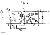
- the feed circuit shown in FIG. 3 also largely corresponds to that of FIG. 1.
- the pulse width modulator 4 is not controlled via one of two further windings of the transformer 6, but in the operating state of the voltage regulation by the output voltage U2 of the supply circuit itself and in the operating state of the power limitation as a function of the output current i2 of the supply circuit.
- the pulse width modulator 4 is controlled by the output current i2 in such a way that the relative switch-on time of the switch 5 becomes increasingly greater with larger output currents i2.
- the voltage divider consisting of resistors 13 and 14 is connected in parallel to output a2, b2 of the supply circuit.
- the resistor 13 is connected via the diode 73 to the beginning, the resistor 14 via the resistor 12 to the end of the secondary winding 62.
- the control input of the pulse width modulator 4 are the two control comparators, each formed by an operational amplifier 32 and 33 upstream.
- the outputs of the control comparators 32 and 33 are brought together via the two diodes 74 and 75.
- the connection point of the diodes 74 and 75 is guided via the resistor 18 a and the light-emitting diode of the optocoupler 8 to a reference potential, namely to the terminal of the capacitor 23 facing away from the diode 9.
- the emitter-collector path of the optocoupler 8 is connected on the emitter side to the connection b1, on the collector side directly to the control input of the pulse duration modulator 4 and via the resistor 11 to the auxiliary voltage + U H.
- the auxiliary voltage U H can be generated in particular with the aid of a further output circuit.
- the control comparator 32 lies with its actual value input or minus input at the tap of the voltage divider consisting of the resistors 13 and 14.
- the reference voltage U Ref1 is at its plus input .
- the actual value input or plus input of the control comparator 33 is connected to the connection of the resistor 12 on the side of the secondary winding 62.
- the reference voltage U Ref2 is at the minus input of the control comparator 33.
- the resistor 12 has the output current i2 flowing through it and forms a current sensor for the output current i2.
- the diodes 74 and 75 lie with their cathodes on the anode of the light-emitting diode of the optocoupler 8 and cause the divided output voltage U2 and the voltage drop across the resistor 12 to be effective in each case the one that would first exceed the associated reference value without regulation .
- the divided output voltage acts as an actual value for voltage regulation and the voltage drop across resistor 12 acts as an actual value for current limitation.
- the supply circuit is particularly suitable for use in devices for remote feeding of intermediate points in devices of electrical or electro-optical communication technology.
Landscapes
- Engineering & Computer Science (AREA)
- Power Engineering (AREA)
- Dc-Dc Converters (AREA)
Claims (9)
- Circuit d'alimentation pour l'alimentation d'au moins un consommateur (V) en une tension continue (U2) obtenue à partir d'un courant continu (i0) indépendant de la charge, comportant un condensateur (21) monté en parallèle à l'entrée (a1, b1) du circuit d'alimentation et un interrupteur (5) qui est susceptible d'être commandé, qui est placé dans une branche du circuit de courant, montée en parallèle à l'entrée (a1, b1) du circuit d'alimentation et qui, au moyen d'un modulateur d'impulsions en durée (4) et en fonction d'une tension (U2, U0) qui dépend de la tension de sortie (U2), est susceptible d'être commandé de telle façon que, dans la plage de réglage du circuit d'alimentation, la durée relative de fermeture de l'interrupteur (5) croît pour des tensions de sortie (U2) croissantes,
caractérisé en ce que l'interrupteur (5) est monté en série avec un enroulement primaire (61) d'un transformateur à accumulation d'énergie (6), et en ce que le circuit d'alimentation comprend au moins un circuit de sortie comportant un enroulement secondaire du transformateur à accumulation d'énergie et une diode (73) polarisée de telle sorte qu'elle est bloquée lorsque l'interrupteur (5) est fermé et conductrice lorsque l'interrupteur (5) est ouvert. - Circuit d'alimentation selon la revendication 1,
caractérisé en ce que,
pour des tensions d'entrée U1 appliquées au niveau du condensateur (21) et qui excèdent une valeur prédéterminée, le modulateur d'impulsions en durée (4) est, en fonction de la tension d'entrée (U1), susceptible d'être commandé de telle sorte que la durée relative de fermeture de l'interrupteur (5) croît pour des tensions d'entrée (U1) croissantes. - Circuit d'alimentation selon la revendication 1 ou 2,
caractérisé en ce que,
la source pour la tension qui est fonction de la tension de sortie est constituée par un enroulement supplémentaire (63) du transformateur à accumulation d'énergie (6). - Circuit d'alimentation selon l'une des revendications 1 à 3,
caractérisé en ce que,
il est prévu, comme source pour une tension qui est proportionnelle à la tension d'entrée, un enroulement supplémentaire (64). - Circuit d'alimentation selon la revendication 3 ou 4,
caractérisé en ce que,
deux branches du circuit de passage du courant, dont chacune est constituée d'un des deux enroulements supplémentaires (63, 64) du transformateur à accumulation d'énergie (6) et d'une diode (71, 72) qui y est montée en série, sont montées entre elles en parallèle de telle sorte que les électrodes des deux diodes (71, 72) de même polarité soient réunies, et en ce que le circuit parallèle des deux branches et un condensateur (22) qui y est monté en parallèle, sont placés entre l'entrée du potentiel de référence et l'entrée de la valeur instantanée d'un comparateur de réglage. - Circuit d'alimentation selon la revendication 2,
caractérisé en ce que,
l'entrée de valeur instantanée d'un comparateur de réglage (31) relié en amont au modulateur d'impulsions en durée (4), est relié, par l'intermédiaire de, respectivement, une diodes (77, 76), à la prise d'un premier diviseur de tension monté en parallèle à l'entrée (a1, b1) et à la prise d'un second diviseur de tension porté à une tension auxiliaire, et en ce que le second diviseur de tension comporte, dans une branche, la section émetteur-collecteur d'un opto-coupleur (8) susceptible d'être commandé par la tension de sortie (U2). - Circuit d'alimentation selon la revendication 1,
caractérisé en ce que,
le modulateur d'impulsions en durée (4) est, d'autre part, susceptible d'être commandé, en fonction du courant de sortie (i2) du circuit d'alimentation, de telle sorte que la durée relative de fermeture de l'interrupteur (5) croît pour des courants de sortie (i2) croissants. - Circuit d'alimentation selon la revendication 7,
caractérisé en ce que,
à l'entrée de commande d'un opto-coupleur (8) relié en amont au modulateur d'impulsions en durée (4), sont reliés en amont deux comparateurs de réglage (32, 33) qui sont réunis par des diodes (74, 75) et parmi lesquels l'un est relié à la prise d'un diviseur de tension (13, 14) monté à la sortie (a2, b2) du montage et l'autre est relié à un détecteur de courant traversé par le courant de sortie (i2). - Circuit d'alimentation selon l'une des revendications 1 à 8,
caractérisé par sa mise en oeuvre dans une installation de téléalimentation de postes intermédiaires dans des installations de la technique de la transmission d'informations par voies électriques ou électro-optiques.
Applications Claiming Priority (2)
| Application Number | Priority Date | Filing Date | Title |
|---|---|---|---|
| DE3802224 | 1988-01-26 | ||
| DE3802224 | 1988-01-26 |
Publications (2)
| Publication Number | Publication Date |
|---|---|
| EP0326064A1 EP0326064A1 (fr) | 1989-08-02 |
| EP0326064B1 true EP0326064B1 (fr) | 1993-06-09 |
Family
ID=6346007
Family Applications (1)
| Application Number | Title | Priority Date | Filing Date |
|---|---|---|---|
| EP89101132A Expired - Lifetime EP0326064B1 (fr) | 1988-01-26 | 1989-01-23 | Circuit d'alimentation pour alimenter au moins une charge avec une source de courant continu |
Country Status (5)
| Country | Link |
|---|---|
| US (1) | US4924369A (fr) |
| EP (1) | EP0326064B1 (fr) |
| JP (1) | JPH01231660A (fr) |
| AU (1) | AU617146B2 (fr) |
| DE (1) | DE58904583D1 (fr) |
Families Citing this family (4)
| Publication number | Priority date | Publication date | Assignee | Title |
|---|---|---|---|---|
| EP0419728A1 (fr) * | 1989-09-29 | 1991-04-03 | Siemens Aktiengesellschaft | Circuit pour alimentation à découpage du type à récupération à fréquence fixe |
| US5448469A (en) * | 1990-02-15 | 1995-09-05 | Deutsche Thomson-Brandt Gmbh | Switch mode power supply with output feedback isolation |
| GB9302942D0 (en) * | 1993-02-13 | 1993-03-31 | Attwood Brian E | Low cost,low current power supply |
| DE102007050620A1 (de) * | 2007-10-23 | 2009-04-30 | Continental Automotive Gmbh | Schaltungsanordnung zum Betreiben einer elektrischen Last und mit Laststrommessung |
Family Cites Families (21)
| Publication number | Priority date | Publication date | Assignee | Title |
|---|---|---|---|---|
| JPS502151A (fr) * | 1973-05-15 | 1975-01-10 | ||
| US4037271A (en) * | 1976-12-03 | 1977-07-19 | Boschert Associates | Switching regulator power supply |
| JPS5378042A (en) * | 1976-12-20 | 1978-07-11 | Sanyo Electric Co Ltd | Switching control type power source circuit |
| US4251857A (en) * | 1979-02-21 | 1981-02-17 | Sperry Corporation | Loss compensation regulation for an inverter power supply |
| JPS56107783A (en) * | 1980-01-31 | 1981-08-26 | Origin Electric Co Ltd | Power converter |
| JPS5932990B2 (ja) * | 1980-02-27 | 1984-08-13 | 横河電機株式会社 | スイッチング・レギュレ−タ |
| GB2073918B (en) * | 1980-04-10 | 1983-10-19 | Standard Telephones Cables Ltd | Dc-dc converter |
| US4320388A (en) * | 1980-07-15 | 1982-03-16 | Westinghouse Electric Corp. | Two wire optical data communication system |
| JPS5728568A (en) * | 1980-07-29 | 1982-02-16 | Toshiba Corp | Self-oscillating type switching regulator |
| US4326532A (en) * | 1980-10-06 | 1982-04-27 | Minnesota Mining And Manufacturing Company | Antithrombogenic articles |
| JPS57202873A (en) * | 1981-06-05 | 1982-12-11 | Sanken Electric Co Ltd | Dc converter |
| DE3221404A1 (de) * | 1982-06-05 | 1983-12-08 | Philips Kommunikations Industrie AG, 8500 Nürnberg | Stromversorgungsschaltung |
| JPS6022467A (ja) * | 1983-07-15 | 1985-02-04 | Nippon Telegr & Teleph Corp <Ntt> | スイツチングレギユレ−タ |
| US4620271A (en) * | 1984-07-13 | 1986-10-28 | Siemens Aktiengesellschaft | Circuit arrangement for feeding electrical users via a switch controller |
| JPS6185068A (ja) * | 1984-08-31 | 1986-04-30 | Fujitsu Ltd | スイツチングレギユレ−タ |
| JPS6225874A (ja) * | 1985-07-25 | 1987-02-03 | Internatl Rectifier Corp Japan Ltd | スイツチング電源用パルス幅変調回路 |
| JPS6264264A (ja) * | 1985-09-13 | 1987-03-23 | Tdk Corp | スイツチング電源 |
| JPS62135270A (ja) * | 1985-12-05 | 1987-06-18 | Nemitsuku Ramuda Kk | 定電圧回路の制御方式 |
| JPS62233067A (ja) * | 1986-03-31 | 1987-10-13 | Toshiba Corp | 安定化電源装置 |
| JPS62281758A (ja) * | 1986-05-29 | 1987-12-07 | Fujitsu Ltd | Dc−dcコンバ−タ |
| US4704670A (en) * | 1986-12-31 | 1987-11-03 | American Telephone & Telegraph Company, At&T Bell Laboratories | Power supply with regulated output voltage |
-
1988
- 1988-11-14 US US07/271,018 patent/US4924369A/en not_active Expired - Fee Related
-
1989
- 1989-01-23 EP EP89101132A patent/EP0326064B1/fr not_active Expired - Lifetime
- 1989-01-23 DE DE8989101132T patent/DE58904583D1/de not_active Expired - Fee Related
- 1989-01-25 AU AU28780/89A patent/AU617146B2/en not_active Ceased
- 1989-01-26 JP JP1015189A patent/JPH01231660A/ja active Pending
Non-Patent Citations (1)
| Title |
|---|
| PATENT ABSTRACTS OF JAPAN, Band 6, Nr. 79 (P-115)[957], 18. Mai 1982; & JP-A-57 14 919 (YOKOGAWA DENKI SEISAKUSHO K.K.) 26-01-1982 * |
Also Published As
| Publication number | Publication date |
|---|---|
| JPH01231660A (ja) | 1989-09-14 |
| DE58904583D1 (de) | 1993-07-15 |
| EP0326064A1 (fr) | 1989-08-02 |
| AU2878089A (en) | 1989-07-27 |
| US4924369A (en) | 1990-05-08 |
| AU617146B2 (en) | 1991-11-21 |
Similar Documents
| Publication | Publication Date | Title |
|---|---|---|
| DE3204840A1 (de) | Gleichstromnetzgeraet mit stromkonstanthaltung, insbeondere fuer eine fernmeldeanlage | |
| DE69733679T2 (de) | Schaltnetzteil | |
| EP0283842A1 (fr) | Convertisseur à découpage et récupération | |
| DE2809138A1 (de) | Stromversorgungseinrichtung | |
| DE3310678C2 (de) | Schaltung zur Regelung der Ausgangsspannung eines elektronischen Schaltnetzteiles | |
| EP0664602B1 (fr) | Convertisseur à récupération avec tension de sortie régulée | |
| DE1513420B2 (de) | Spannungsregeleinrichtung zur erzeugung einer geregelten gleichspannung mit einem schalttransistor und einem kontinuierlich gesteuerten stelltransistor | |
| EP0326064B1 (fr) | Circuit d'alimentation pour alimenter au moins une charge avec une source de courant continu | |
| EP0099596A1 (fr) | Circuit d'alimentation en courant électrique | |
| DE2808156C2 (de) | Elektronisches, berührungslos wirkendes, zweipoliges Schaltgerät | |
| EP0524425A1 (fr) | Arrangement de circuit pour limiter le courant lors de la fermeture du circuit et pour la protection contre surtension pour dispositif d'alimentation à découpage | |
| EP0266743B1 (fr) | Disposition de circuit pour produire une tension d'alimentation interne dans une alimentation de courant à découpage | |
| DE2611439C2 (de) | Leistungsversorgungsschaltkreis mit hohem Wirkungsgrad | |
| EP0657987B1 (fr) | Convertisseur à découpage avec limitation de courant | |
| DE4028471C2 (fr) | ||
| EP0302433B1 (fr) | Convertisseur à récupération | |
| EP0581989B1 (fr) | Régulateur à découpage avec régulation d'au moins une tension de sortie | |
| DE4106915C2 (fr) | ||
| EP0499024A2 (fr) | Dispositif de circuit pour un convertisseur de courant continu | |
| EP0657986B1 (fr) | Convertisseur à découpage avec coupleur optique | |
| DE4017374C2 (de) | Gleichspannungswandler | |
| DE2826349C2 (de) | Wechselrichter in Multivibrator-Schaltung | |
| EP0576706B1 (fr) | Circuit d'alimentation en courant avec un minimum de deux sorties | |
| EP0576702A1 (fr) | Convertisseur à découpage avec limitation de courant | |
| EP0584623A1 (fr) | Convertisseur en courant continu à mode de courant |
Legal Events
| Date | Code | Title | Description |
|---|---|---|---|
| PUAI | Public reference made under article 153(3) epc to a published international application that has entered the european phase |
Free format text: ORIGINAL CODE: 0009012 |
|
| AK | Designated contracting states |
Kind code of ref document: A1 Designated state(s): DE FR GB IT |
|
| 17P | Request for examination filed |
Effective date: 19900126 |
|
| 17Q | First examination report despatched |
Effective date: 19910918 |
|
| GRAA | (expected) grant |
Free format text: ORIGINAL CODE: 0009210 |
|
| AK | Designated contracting states |
Kind code of ref document: B1 Designated state(s): DE FR GB IT |
|
| REF | Corresponds to: |
Ref document number: 58904583 Country of ref document: DE Date of ref document: 19930715 |
|
| ITF | It: translation for a ep patent filed | ||
| GBT | Gb: translation of ep patent filed (gb section 77(6)(a)/1977) |
Effective date: 19930813 |
|
| ET | Fr: translation filed | ||
| PGFP | Annual fee paid to national office [announced via postgrant information from national office to epo] |
Ref country code: GB Payment date: 19931220 Year of fee payment: 6 |
|
| PGFP | Annual fee paid to national office [announced via postgrant information from national office to epo] |
Ref country code: FR Payment date: 19940121 Year of fee payment: 6 |
|
| PGFP | Annual fee paid to national office [announced via postgrant information from national office to epo] |
Ref country code: DE Payment date: 19940322 Year of fee payment: 6 |
|
| PLBE | No opposition filed within time limit |
Free format text: ORIGINAL CODE: 0009261 |
|
| STAA | Information on the status of an ep patent application or granted ep patent |
Free format text: STATUS: NO OPPOSITION FILED WITHIN TIME LIMIT |
|
| 26N | No opposition filed | ||
| PG25 | Lapsed in a contracting state [announced via postgrant information from national office to epo] |
Ref country code: GB Effective date: 19950123 |
|
| GBPC | Gb: european patent ceased through non-payment of renewal fee |
Effective date: 19950123 |
|
| PG25 | Lapsed in a contracting state [announced via postgrant information from national office to epo] |
Ref country code: FR Effective date: 19950929 |
|
| PG25 | Lapsed in a contracting state [announced via postgrant information from national office to epo] |
Ref country code: DE Effective date: 19951003 |
|
| REG | Reference to a national code |
Ref country code: FR Ref legal event code: ST |
|
| PG25 | Lapsed in a contracting state [announced via postgrant information from national office to epo] |
Ref country code: IT Free format text: LAPSE BECAUSE OF NON-PAYMENT OF DUE FEES;WARNING: LAPSES OF ITALIAN PATENTS WITH EFFECTIVE DATE BEFORE 2007 MAY HAVE OCCURRED AT ANY TIME BEFORE 2007. THE CORRECT EFFECTIVE DATE MAY BE DIFFERENT FROM THE ONE RECORDED. Effective date: 20050123 |