EP0326192A2 - Films minces magnétorésistifs couplés pour détection de flux magnétique - Google Patents
Films minces magnétorésistifs couplés pour détection de flux magnétique Download PDFInfo
- Publication number
- EP0326192A2 EP0326192A2 EP89105527A EP89105527A EP0326192A2 EP 0326192 A2 EP0326192 A2 EP 0326192A2 EP 89105527 A EP89105527 A EP 89105527A EP 89105527 A EP89105527 A EP 89105527A EP 0326192 A2 EP0326192 A2 EP 0326192A2
- Authority
- EP
- European Patent Office
- Prior art keywords
- magnetic
- films
- axis
- along
- easy axis
- Prior art date
- Legal status (The legal status is an assumption and is not a legal conclusion. Google has not performed a legal analysis and makes no representation as to the accuracy of the status listed.)
- Withdrawn
Links
- 230000005291 magnetic effect Effects 0.000 title claims description 101
- 230000004907 flux Effects 0.000 title claims description 18
- 239000010409 thin film Substances 0.000 title claims description 8
- 239000010408 film Substances 0.000 claims description 111
- 230000008878 coupling Effects 0.000 claims description 27
- 238000010168 coupling process Methods 0.000 claims description 27
- 238000005859 coupling reaction Methods 0.000 claims description 27
- 239000013598 vector Substances 0.000 claims description 26
- 230000005415 magnetization Effects 0.000 claims description 11
- 238000000034 method Methods 0.000 claims description 8
- 230000000694 effects Effects 0.000 description 18
- 230000005330 Barkhausen effect Effects 0.000 description 14
- 230000001939 inductive effect Effects 0.000 description 7
- 239000000758 substrate Substances 0.000 description 7
- RTAQQCXQSZGOHL-UHFFFAOYSA-N Titanium Chemical compound [Ti] RTAQQCXQSZGOHL-UHFFFAOYSA-N 0.000 description 6
- 239000010936 titanium Substances 0.000 description 6
- 229910052719 titanium Inorganic materials 0.000 description 6
- 239000000463 material Substances 0.000 description 5
- VYPSYNLAJGMNEJ-UHFFFAOYSA-N Silicium dioxide Chemical compound O=[Si]=O VYPSYNLAJGMNEJ-UHFFFAOYSA-N 0.000 description 4
- 230000008901 benefit Effects 0.000 description 4
- 239000004020 conductor Substances 0.000 description 4
- 230000035945 sensitivity Effects 0.000 description 4
- 239000007787 solid Substances 0.000 description 4
- 230000008859 change Effects 0.000 description 3
- 230000000295 complement effect Effects 0.000 description 3
- 230000006870 function Effects 0.000 description 3
- 230000001965 increasing effect Effects 0.000 description 3
- 238000004519 manufacturing process Methods 0.000 description 3
- 230000002829 reductive effect Effects 0.000 description 3
- 230000004044 response Effects 0.000 description 3
- 229920006395 saturated elastomer Polymers 0.000 description 3
- PXHVJJICTQNCMI-UHFFFAOYSA-N Nickel Chemical compound [Ni] PXHVJJICTQNCMI-UHFFFAOYSA-N 0.000 description 2
- 238000005516 engineering process Methods 0.000 description 2
- 229910052710 silicon Inorganic materials 0.000 description 2
- 239000010703 silicon Substances 0.000 description 2
- 235000012239 silicon dioxide Nutrition 0.000 description 2
- 239000000377 silicon dioxide Substances 0.000 description 2
- 238000003860 storage Methods 0.000 description 2
- 229910000640 Fe alloy Inorganic materials 0.000 description 1
- 230000009471 action Effects 0.000 description 1
- 238000007792 addition Methods 0.000 description 1
- 230000015572 biosynthetic process Effects 0.000 description 1
- 229910052729 chemical element Inorganic materials 0.000 description 1
- 238000010276 construction Methods 0.000 description 1
- 230000003247 decreasing effect Effects 0.000 description 1
- 238000005137 deposition process Methods 0.000 description 1
- 238000004870 electrical engineering Methods 0.000 description 1
- 239000012212 insulator Substances 0.000 description 1
- UGKDIUIOSMUOAW-UHFFFAOYSA-N iron nickel Chemical compound [Fe].[Ni] UGKDIUIOSMUOAW-UHFFFAOYSA-N 0.000 description 1
- 230000005381 magnetic domain Effects 0.000 description 1
- 239000000696 magnetic material Substances 0.000 description 1
- 230000007246 mechanism Effects 0.000 description 1
- 229910052759 nickel Inorganic materials 0.000 description 1
- 239000000615 nonconductor Substances 0.000 description 1
- 238000004806 packaging method and process Methods 0.000 description 1
- 230000036961 partial effect Effects 0.000 description 1
- 229910000889 permalloy Inorganic materials 0.000 description 1
- 230000035699 permeability Effects 0.000 description 1
- 238000002360 preparation method Methods 0.000 description 1
- 238000003672 processing method Methods 0.000 description 1
- 230000000135 prohibitive effect Effects 0.000 description 1
- 230000009467 reduction Effects 0.000 description 1
- 238000009738 saturating Methods 0.000 description 1
- 239000004065 semiconductor Substances 0.000 description 1
- 238000000926 separation method Methods 0.000 description 1
- 230000003068 static effect Effects 0.000 description 1
- 230000007704 transition Effects 0.000 description 1
Images




Classifications
-
- G—PHYSICS
- G11—INFORMATION STORAGE
- G11B—INFORMATION STORAGE BASED ON RELATIVE MOVEMENT BETWEEN RECORD CARRIER AND TRANSDUCER
- G11B5/00—Recording by magnetisation or demagnetisation of a record carrier; Reproducing by magnetic means; Record carriers therefor
- G11B5/127—Structure or manufacture of heads, e.g. inductive
- G11B5/33—Structure or manufacture of flux-sensitive heads, i.e. for reproduction only; Combination of such heads with means for recording or erasing only
- G11B5/39—Structure or manufacture of flux-sensitive heads, i.e. for reproduction only; Combination of such heads with means for recording or erasing only using magneto-resistive devices or effects
- G11B5/3903—Structure or manufacture of flux-sensitive heads, i.e. for reproduction only; Combination of such heads with means for recording or erasing only using magneto-resistive devices or effects using magnetic thin film layers or their effects, the films being part of integrated structures
- G11B5/3906—Details related to the use of magnetic thin film layers or to their effects
- G11B5/3945—Heads comprising more than one sensitive element
- G11B5/3948—Heads comprising more than one sensitive element the sensitive elements being active read-out elements
- G11B5/3951—Heads comprising more than one sensitive element the sensitive elements being active read-out elements the active elements being arranged on several parallel planes
-
- G—PHYSICS
- G11—INFORMATION STORAGE
- G11B—INFORMATION STORAGE BASED ON RELATIVE MOVEMENT BETWEEN RECORD CARRIER AND TRANSDUCER
- G11B19/00—Driving, starting, stopping record carriers not specifically of filamentary or web form, or of supports therefor; Control thereof; Control of operating function ; Driving both disc and head
- G11B19/02—Control of operating function, e.g. switching from recording to reproducing
- G11B19/04—Arrangements for preventing, inhibiting, or warning against double recording on the same blank or against other recording or reproducing malfunctions
-
- G—PHYSICS
- G11—INFORMATION STORAGE
- G11B—INFORMATION STORAGE BASED ON RELATIVE MOVEMENT BETWEEN RECORD CARRIER AND TRANSDUCER
- G11B5/00—Recording by magnetisation or demagnetisation of a record carrier; Reproducing by magnetic means; Record carriers therefor
- G11B5/127—Structure or manufacture of heads, e.g. inductive
- G11B5/33—Structure or manufacture of flux-sensitive heads, i.e. for reproduction only; Combination of such heads with means for recording or erasing only
- G11B5/332—Structure or manufacture of flux-sensitive heads, i.e. for reproduction only; Combination of such heads with means for recording or erasing only using thin films
-
- G—PHYSICS
- G11—INFORMATION STORAGE
- G11B—INFORMATION STORAGE BASED ON RELATIVE MOVEMENT BETWEEN RECORD CARRIER AND TRANSDUCER
- G11B5/00—Recording by magnetisation or demagnetisation of a record carrier; Reproducing by magnetic means; Record carriers therefor
- G11B5/127—Structure or manufacture of heads, e.g. inductive
- G11B5/33—Structure or manufacture of flux-sensitive heads, i.e. for reproduction only; Combination of such heads with means for recording or erasing only
- G11B5/39—Structure or manufacture of flux-sensitive heads, i.e. for reproduction only; Combination of such heads with means for recording or erasing only using magneto-resistive devices or effects
- G11B5/3903—Structure or manufacture of flux-sensitive heads, i.e. for reproduction only; Combination of such heads with means for recording or erasing only using magneto-resistive devices or effects using magnetic thin film layers or their effects, the films being part of integrated structures
- G11B5/3967—Composite structural arrangements of transducers, e.g. inductive write and magnetoresistive read
-
- G—PHYSICS
- G11—INFORMATION STORAGE
- G11B—INFORMATION STORAGE BASED ON RELATIVE MOVEMENT BETWEEN RECORD CARRIER AND TRANSDUCER
- G11B5/00—Recording by magnetisation or demagnetisation of a record carrier; Reproducing by magnetic means; Record carriers therefor
- G11B5/127—Structure or manufacture of heads, e.g. inductive
- G11B5/33—Structure or manufacture of flux-sensitive heads, i.e. for reproduction only; Combination of such heads with means for recording or erasing only
- G11B5/39—Structure or manufacture of flux-sensitive heads, i.e. for reproduction only; Combination of such heads with means for recording or erasing only using magneto-resistive devices or effects
- G11B5/3903—Structure or manufacture of flux-sensitive heads, i.e. for reproduction only; Combination of such heads with means for recording or erasing only using magneto-resistive devices or effects using magnetic thin film layers or their effects, the films being part of integrated structures
- G11B5/399—Structure or manufacture of flux-sensitive heads, i.e. for reproduction only; Combination of such heads with means for recording or erasing only using magneto-resistive devices or effects using magnetic thin film layers or their effects, the films being part of integrated structures with intrinsic biasing, e.g. provided by equipotential strips
Definitions
- This invention relates to magnetic read-write head structures in general, to magneto-resistive thin film head structures in particular and to twin track recording techniques.
- This application is related to my own co-pending, commonly assigned application number 83104300.5 relating to the generic twin track recording method and number 83104293.2 relating to a twin track read head structure employing magnetically sensitive transistors as a sensitive element.
- a wide variety of magnetic read-write head structures exists.
- the structures which are adapted for both reading and writing employ one of several technologies such as inductive, magneto-resistive or other solid state (Hall or magnetic transistor) sensors.
- the preferred embodiment described herein addresses several problems with the known prior art.
- U. S. Patent 4,413,296 illustrates a single track read head employing a thin film magneto-resistive sensing element.
- no means is provided for establishing and maintaining an anti-parallel magnetic couple having the preferred magnetization orientation directed along the easy axis of the MR films.
- Barkhausen noise will be present from the shifting multidomain walls.
- the Barkhausen noise effect is a particularly significant problem as will be appreciated by those of skill in the art.
- the difficulties in establishing a single domain magnetic film are technically prohibitive at present.
- demagnetizing fields are automatically created in both films whenever external magnetic fields are applied along either the X or Y axis.
- the demagnetizing fields will be evident at the edges or ends of the films and will tend to create multidomain walls with the attendant increase in Barkhausen noise.
- Barkhausen noise As the relative size of such sensors is reduced to accommodate smaller recording tracks with the consequent higher density, the effects of the Barkhausen noise become overwhelmingly important.
- a further problem with known prior art magneto-resistive or inductive or solid state magnetic read-write head structures is that the sensor element must often be placed in very close proximity to the magnetic record in order to experience enough magnetic flux to provide a usable output. This results in problems with head to recording medium contact and wear problems well known to those skilled in the field. It would be desirable to remove the sensitive element to an elevation above the recording medium without reducing the sensitivity thereof.
- US-A-4141051 shows a magnetic reading head with a magneto-resistive element whose easy-axis of magnetisation is not parallel to the direction of the measuringcurrent.
- the head uses just one film of magneto-resistive material.
- US-A-4488194 there is disclosed a magneto-resistive element with the easy-axis of magnetisation perpendicular to the plane of the recording medium and to the direction of the current flow along its length.
- the magneto-resistive film is coupled to a single domain magnetic film and it is only sensitive to a field parallel to the easy-axis of magnetisation.
- a primary object of the present invention is to provide an improved magneto-resistive twin coupled film read head structure in which means are provided for creating and maintaining a preferred magnetic anti-parallel couple in the films along the desired easy axis.
- the foregoing and still other objects of this invention which have not been enumerated are provided in an improved read-write head structure using a vertical twin track reading and writing method.
- the structure employs a generally U-shaped inductive read-write mechanism which may preferably be employed in tandem with a second U-shaped structure incorporating a coupled thin film magneto-resistive sensor having the easy axis of magnetization arranged perpendicular to the direction of current passage through the sensor. This achieves a balanced demagnetizing effect that eliminates or greatly reduces the tendency to create multiple domain walls and to reduce or eliminate Barkhausen noise.
- the inductive read-write structure portion may be employed during read back to magnetically bias the MR structure portion so that the MR films will be bidirectionally sensitive to magnetic flux.
- a sustaining current may be passed through the MR device films to establish the anti-parallel couple along a preferred axis arranged orthogonal to the direction of passage of flux through the thin films.
- FIG 1 a generic form of the preferred embodiment of the present invention is described in the schematic view.
- a substrate 1 of non-magnetic material which may preferably be silicon or the like for ease in constructing the other elements of the read-write head using semiconductor processing methods, is shown.
- the substrate 1 has deposited on its upper surface a magnetically permeable generally U-shaped structure 2.
- This is schematically shown as being provided with a coil 3 and contacts 4 for energizing the coil 3 electrically.
- the magnetically permeable member 2 is generally configured in a U shape and has two legs 5 which may interface a magnetic recording medium or, as shown in Figure 1A, a second magnetically permeable structure.
- the legs 5 are generally oriented parallel to one another and are so arranged that their long dimension is in the plane of the drawing 1A at the end faces 5A.
- the footprint of these surfaces 5A upon the second magnetically permeable member 6 or upon a magnetic recording medium shows the generic orientation of the twin track vertically polarized read-write system as depicted in Figure 2A. This footprint has the long dimensions of each of the legs 5A shaded as shown. It will be observed that the projections of the legs 5A upon a plane of the recording medium have their maximum dimensions each lying in the same common plane perpendicular to the plane of the recording medium. This distinguishes the two legs and their orientation with respect to each other and to a recording medium from the usual two-leg structure such as that shown in U. S. Patent 4,413,296 mentioned previously in which the maximum dimensions of the end faces of the read-write head will be footprints that are parallel to each other and cannot lie in the same plane arranged vertically to the plane of the recording medium.
- a second magnetically permeable member 6 having two magnetically permeable legs 7 is shown.
- a bridging member 8 comprising a coupled film magneto-resistive sensor element of a preferred form in accordance with the invention is also illustrated.
- Contacts 9 provide means of energizing the MR film element 8 across the bridge between legs 7 to provide output signals.
- the end faces of the second magnetically permeable member 6 are shown as end faces 6A and these would confront a magnetic recording medium having a footprint thereon as shown in Figure 2A.
- the substrate 1 may be a semiconductive material such as silicon in its intrinsic state, i.e., without doping so that it is essentially a non-conductor or insulator. This is convenient and facilitates fabrication of the magnetically permeable elements and the MR elements utilizing planar deposition processes usually employed in the semiconductive LSI industry.
- magneto-resistive coupled film elements shown generically as the bridging element 8 between the legs 7 of the second magnetically permeable structure 6 are shown in the cross-section 1B as two adjacent layers.
- the actual structure will be described in greater detail but it should be pointed out that an insulative layer 10 of silicon dioxide or the like may be used to electrically separate the magnetically sensitive MR legs 8 from the coupling legs 7 of the second magnetically permeable structure 6.
- the first and second magnetically permeable members 2 and 6 may preferably be constructed of permalloy, which is a nickel, iron alloy well known in the field. It will also be observed that there is a reluctance path between the legs 7 and the bridging member 8 which comprises the MR sensor and the amount and relative magnitude of this reluctance in proportion to the reluctance of the gap between the surfaces 5A and the top surface of the element 6 is also important as will be described later. In addition, there is a variable reluctance of the MR bridging element 8 which must be taken into account as will be later described.
- FIG. 1C an enlarged cross-section along lines AA in Figure 1A is illustrated.
- the magneto-resistive element comprising the twin coupled films 8 is shown in greater detail. They are deposited along the insulative layer 10 to separate them from the substrate 1 in the electrical sense.
- the two magnetic films 8 are also separated from one another by a thin, non-magnetically permeable conductor such as a titanium layer.
- the titanium layer may, however, be in electrical contact if desired.
- the relative thicknessess of the various layers have some importance in establishing the coupled anti-parallel magnetic pair in the films 8.
- the magnetic films may be nickel iron of approximately 200 Angstrom units thickness each and the magnetically permeable members shown in Figures 1A and 1B may be the permaloy material of approximately 3000 Angstrom units thickness.
- the layers 10 shown in Figure 1B and 1C may be illustratively 1000 Angstrom units thickness silicon dioxide.
- FIG 1D a magnetic film pair 8 having an electrical current directed into the plane of the paper as shown by the conventional circle with an X in it are illustrated.
- the anti-parallel magnetic couple is established by passing a current in the direction shown which creates the magnetic vectors H12 and H21 in the left and right films, respectively. These are shown by the vector arrows so labeled.
- a closed magnetic path exists with the complementary poles closed through the air gap at each end between the two films. This closure takes place in the structure shown in Figure 1C through the 300 Angstrom unit thick titanium layer.
- the end faces 6A of the second magnetically permeable structure would interface a magnetically recorded medium such as that shown in Figure 2A and 2B and the resultant flux from the complementarily poled transitions as shown in 2A would be coupled through the end faces 6A of the legs 7 in the second permeable magnetic structure 6 and would pass through the insulative layer 10 shown in Figure 1B and longitudinally through the magnetically sensitive MR film pair 8.
- This would be a direction generally orthogonal to the chosen easy axis and parallel with the axis of signal current through the MR film pair and is a distinct departure from the arrangements in the prior art.
- the magnetically sensitive magneto-resistive material layers 8 are separated by a titanium layer as shown in Figure 1C as layer 11. However, where the magnetically sensitive elements overlie the coupling legs 7, the titanium layer 11 is removed and the legs 8 are in electrical contact with one another, generally in the region shown as contact areas 9 in Figure 1A. Thus, a current may be passed through the elements 8 in the direction such as that depicted in Figure 1A by the current vector I s which is also shown in the cross-sectional Figure 1D. This is the sustaining current for creating the anti-parallel magnetic couple in the twin magneto-resistive films 8.
- the operation of the structure depicted in Figures 1A through 1D will be described in greater detail shortly. First, however, it is necessary to discuss some of the prior art arrangements of coupled magnetic film pair sensors utilized in various read head embodiments of the prior art.
- FIG. 3A an anti-parallel coupled film pair 12 is depicted.
- the magnetic anti-parallel vectors M1 and M2 are shown as oppositely directed.
- the topmost layer has the solid arrow M1 and the bottom layer has the dotted arrow M2 as shown in Figure 3A.
- the contacts 13 facilitate passage of a bias current through the MR pair 12 along the easy axis which is shown to be parallel with the long dimension of the pair as depicted in Figure 3A.
- Figure 4 illustrates schematically a pair of magneto-resistive films 12 electrically connected through contacts 13 and an auxiliary conductor 14 as shown in U. S. Patent 4,413,296.
- the easy axis of magnetization is chosen as shown in that patent to be parallel with the long axis of the film pair 12.
- Current I may be passed through the pair in the path which is facilitated by the contacts 13 and the conductor 14 as illustrated. This will result in the anti-parallel couple M1 M2 being torqued by equal but opposite amounts to modify the angle 1 2 in similar fashion as was discussed with respect to Figure 3B. This is true since no means is provided for establishing the anti-parallel magnetic couple with the preferred magnetization orientation lying along the easy axis.
- the easy axis is preferably not located along the X axis as shown in Figure 4. It will be canted at some small angle as described in that patent. This has the net result of making the film structures bidirectionally sensitive which is indeed a good advantage so that the sense currents flowing from the respective films are provided with the same spatial direction of flow and mutual biasing of these two structures (i.e., mutual coupling therebetween) is avoided.
- the anti-parallel couple is formed by permanently magnetizing the films in opposite direction when they are originally created.
- the imbalance in demagnetizing fields experienced when externally applied fields are imposed on the structure may disorient and eventually disrupt the preferred anti-parallel couple which will result in reduction in sensitivity and increase in noise.
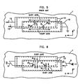
- Figure 5 illustrates another prior art twin film pair 12 arranged in an electrical connection pattern which is different from that shown in Figure 4.
- the contacts 13 direct biasing current I through parallel films 12 in the same direction.
- the easy axis is assumed to be along the X axis and the passage of the current I will torque the magnetic vectors M1 and M2 through angles ⁇ 1 and ⁇ 2, respectively.
- a significant advantage is that the output will be differen tial and may be conveniently measured between the two output terminals 13 which are not connected to ground.
- no means has been provided for establishing and maintaining the preferred anti-parallel magnetic vector couple with a preferred orientation along the easy axis.
- demagnetizing fields When externally applied magnetic fields are directed along either the X or Y axis, demagnetizing fields will be introduced in both films 12 resulting from the different effect of the angles ⁇ 1 and ⁇ 2 as discussed with respect to Figure 3 previously. In addition, Barkhausen noise will be present where multi-domains exist within the films 12 in Figure 5. Indeed, the effect of the demagnetizing fields created by the application of external magnetic fields to be sensed by the films will tend to create or move domain walls within the films and more particularly so as the size of the films is reduced to accommodate higher and higher density recording patterns.
- FIG 6 a schematic view similar to Figures 3 through 5 is shown for the magneto-resistive sensor technology utilized in the present invention.
- the electrical contacts 9 are utilized for supplying the bias current I along the hard axis (X axis) of the coupled films 8.
- the easy axis is located along the Y direction which is perpendicular to the axis on which the bias current is supplied.
- the mutual field coupling between the film layers 8 in the presence of current I flowing longitudinally along the X axis establishes and maintains the easy axis anti-parallel couple in a prescribed direction as previously discussed with respect to Figure 1D.
- the anti-parallel magnetic vectors M1 M2 are stable and balanced so long as the current I flows through each of the layers 8.
- a read head employs a coupled pair of magnetic film elements having their magnetic anisotropy in the easy axis running in a direction perpendicular to the axis on which both the bias and signal current is supplied, i.e., along the hard axis.
- Such devices as sensitive to magnetic fields applied along the hard axis and respond in a balanced and stable fashion without creating demagnetizing fields, multiple domain walls and concommitant Barkhausen noise effects.
- the method of biasing the magnetically coupled vectors in the twin films of an MR sensor uses a separate parallel conductive plane carrying a bias current I b .
- the sustaining current I s for creating the preferred easy axis stable couple is shown applied to contacts 9 and passing along the hard axis of the coupled films 8 as was the case for Figure 6.
- a conductive plane 14 is shown. This plane is to overlie the coupled pair 8 and to conduct current I b in a direction perpendicular to the hard axis which is, of course, the signal current axis or long axis of the MR films. This will set up a bias field H along the hard axis and torque the preferred couple through an angle when I b is flowing.
- the plane 14 is to be electrically insulated from the MR films 8 as well be readily apparent. For ease in construction and proper function, the plane 14 overlies both films and is not sandwiched between the films.
- Such structures as depicted in Figures 6 and 11 may be embodied in an improved read-write head as shown in Figures 1A through 1D to which reference is again made.
- the first magnetically permeable structure element 2 forms a closure or keeper path for a write current magnetic field that will be coupled through the air gap at the end faces 5A to the coupling leg 7.
- a magnetizing coil 3 energized through contacts 4 encircles the central portion of the top magnetically permeable member.
- the coil 3 has two functions. During reading operation, a unidirectional fixed bias field current is conducted by coil 3. This has the purpose of creating the magnetic vector H shown in Figure 6 for rotating the magnetization vectors within each of the MR films 8 by the angle ⁇ . This rotation of the magnetic vectors away from the easy axis by an angle approximately ⁇ /4 radians allows the magneto-resistive films 8 to respond to magnetic fields applied in either direction along the hard axis.
- Magnetic fields coupled from the pole faces 6A at the end of the second magnetically permeable member 6 are conducted by the coupling legs 7 up to and through the MR film layers 8 which bridge between the two coupling legs 7 and complete the magnetically permeable member 6.
- Magnetic flux from a recorded magnetic medium will circulate through the contours C, A, B, D or D, B, A, C depending upon the polarity recorded in the tracks such as shown in Figure 2A.
- the second function of the coil 3 is for writing new data in a vertically recordable magnetic medium.
- electrical current considerably in excess of the bias current used during reading is passed through coil 3 by means of the contacts 4.
- the effect of this electrical current is to magnetize the first magnetically permeable member 2 which will result in two oppositely polarized regions being written in a magnetic medium if the pole faces 5A at the ends of the coupling legs 5 are in proximity to a medium. From this it is evident that the first magnetically permeable member with its coil 3 may be used in the ordinary sense as an inductive read-write head.
- the magnetic flux generated at the faces 5A is impressed upon the second magnetically permeable member 6 and passes through the coupling legs 7 to magnetize the magnetic medium (not shown in Figure 1A) at its areas adjacent to the faces 6A.
- some of the flux is conducted through the bridging element comprising the magnetic resistive layers 8 that completes the second magnetically permeable member 6.
- saturation occurs and once a critical value has been reached, no further flux is conducted by the coupling members 8.
- the MR sensor leg comprising the MR film pairs 8 is saturated. That is, magnetization within the MR films 8 is forced to lie essentially along the hard magnetic axis and no additional flux will be passed once this level has been reached. This is illustrated in Figure 9 and will be discussed.
- MR films allow a critical writing field to be coupled to the magnetic medium once a critical coil current has been achieved in coil 3 in Figure 1A.
- the permeability of the magneto-resistive film elements 8 when viewed along the hard axis is similar to an air gap once saturation has been achieved. It will be observed that the field seen by the magnetic medium at the interface with faces 6A of the second magnetic permeable member is quite low until a critical coil current for coil 3 is reached. At approximately 40 milliamperes as shown in Figure 9, the MR films 8 will be saturated in the hard direction and will not further conduct flux. Any additional bias current or write current applied to coil 3 will result in coupling magnetic flux to the medium through the coupling legs 7 and not shunting it through the MR film pair 8.
- a gap between the top keeper or driver member described as the first magnetically permeable member 2 and the vertical coupling leg 7 will minimize shunting of field coupled from the magnetic storage medium through legs 7 to permit it to pass through the MR elements completing the second magnetically permeable member 6.
- the gap also regulates the amount of electrical current needed to write data into the storage medium because it minimizes the changing reluctance effects between the vertical legs 7 of the second magnetically permeable structure and the recording medium due to a variable flying height that occurs during the writing mode. If the gap between the first and second magnetically permeable elements 2 and 6 respectively did not exist, then the sensor elements 8 would only experience a small fraction of the signal field coupled from the medium through the vertical legs 7.
- the MR films 8 represent a reluctance that depends upon the level of magnetic flux being conducted.
- the reluctance is approximately equivalent to an air gap. Below saturation, the reluctance is variable in a more or less linear fashion that is utilized during read back. There is also a third magnetic reluctance between the end faces 6A of the second magnetically permeable member and the surface of the recording medium.
- the reluctances must be carefully chosen relative to one another such that the first reluctance between the first magnetic member and the second magnetically permeable member during reading is greater than the second magnetic reluctance between the ends of the MR film elements 8 which in turn should be less than the reluctance between the end faces 6A of the coupling legs 7 and the surface of the recording medium. This guarantees that flux coupled from the medium will be conducted preferentially through the MR films 8 and will not be shunted away through the first keeper member of magnetically permeable material 2 during the readback mode.
- the reluctance of the coupling between the legs 7 increases to be approximately that of an air gap when the MR elements 8 are saturated. This has the effect of increasing the reluctance there to a level greater than that between the end faces 6A and the record medium so that during the writing mode, flux is effectively coupled back to the medium instead of being shunted away through the MR legs 8.
- the overall design illustrated in Figure 1A also solves some of the other problems with the prior art.
- the fundamental physical problem of lapping the end faces and wear problems associated with the end faces of the coupling pole members where they are near the magnetic medium is solved since any wear that occurs on the magnetically permeable coupling legs 7 does not affect the sensor area in the film elements 8A.
- the first magnetically permeable member 2 having coil 3 wrapped about it and end faces 5A at the ends of the coupling legs 5 could be used in its own right to read and write magnetic twin tracks on a vertically recordable medium.
- FIG. 1A a second magnetically permeable member 6 has coupling legs 7 and sensor legs 8 bridging the coupling legs 7 employed as described.
- the sensing leg 8 may comprise not just the MR sensors disclosed but may incorporate a gap with a magnetic solid state sensor such as a magnetic transistor, Hall cell or the like placed therein. The size of the gap and the reluctance would have to be adjusted to accommodate writing and reading as previously described so long as the reluctance values relative to one another are maintained as previously described.
- FIG. 10 A preferred embodiment of a final read-write head design in accordance with the principles described herein is shown in Figure 10.
- coupling legs 7 are angled to bring their end faces 6A closer together at the interface of the magnetic recording medium. This establishes the recording track separation distance as shown in Figure 2A.
- a coil 3 is borne upon an elongated section of the first magnetically permeable member 2 to accommodate a greater number of turns.
- the MR film element layers 8 are elongated relative to the distance between the end faces 6A to increase the signal output.
Landscapes
- Engineering & Computer Science (AREA)
- Manufacturing & Machinery (AREA)
- Magnetic Heads (AREA)
- Hall/Mr Elements (AREA)
Priority Applications (1)
| Application Number | Priority Date | Filing Date | Title |
|---|---|---|---|
| EP89105527A EP0326192A3 (fr) | 1984-02-28 | 1984-12-04 | Films minces magnétorésistifs couplés pour détection de flux magnétique |
Applications Claiming Priority (3)
| Application Number | Priority Date | Filing Date | Title |
|---|---|---|---|
| US06/584,364 US4626946A (en) | 1984-02-28 | 1984-02-28 | Twin track vertical read-write head structure |
| US584364 | 1984-02-28 | ||
| EP89105527A EP0326192A3 (fr) | 1984-02-28 | 1984-12-04 | Films minces magnétorésistifs couplés pour détection de flux magnétique |
Related Parent Applications (2)
| Application Number | Title | Priority Date | Filing Date |
|---|---|---|---|
| EP84114664.0 Division | 1984-12-04 | ||
| EP84114664A Division EP0154005B1 (fr) | 1984-02-28 | 1984-12-04 | Structure de tête de lecture/écriture pour enregistrement à deux pistes |
Publications (2)
| Publication Number | Publication Date |
|---|---|
| EP0326192A2 true EP0326192A2 (fr) | 1989-08-02 |
| EP0326192A3 EP0326192A3 (fr) | 1989-09-06 |
Family
ID=26120023
Family Applications (1)
| Application Number | Title | Priority Date | Filing Date |
|---|---|---|---|
| EP89105527A Withdrawn EP0326192A3 (fr) | 1984-02-28 | 1984-12-04 | Films minces magnétorésistifs couplés pour détection de flux magnétique |
Country Status (1)
| Country | Link |
|---|---|
| EP (1) | EP0326192A3 (fr) |
Cited By (4)
| Publication number | Priority date | Publication date | Assignee | Title |
|---|---|---|---|---|
| US5307226A (en) * | 1992-06-05 | 1994-04-26 | Hewlett-Packard Company | Improved magnetoresistive transducer with substantially perpendicular easy axis |
| EP0651374A3 (fr) * | 1993-11-01 | 1995-09-06 | Hewlett Packard Co | Une tête magnétorésistive planaire. |
| EP0598581A3 (en) * | 1992-11-17 | 1995-10-04 | Ibm | Magnetoresistive sensor. |
| EP0780833A3 (fr) * | 1995-12-20 | 1999-01-07 | Ampex Corporation | Système d'enregistrement magnétique amélioré à couche saturable et détection utilisant un élément MR |
Family Cites Families (2)
| Publication number | Priority date | Publication date | Assignee | Title |
|---|---|---|---|---|
| US3860965A (en) * | 1973-10-04 | 1975-01-14 | Ibm | Magnetoresistive read head assembly having matched elements for common mode rejection |
| US4356523A (en) * | 1980-06-09 | 1982-10-26 | Ampex Corporation | Narrow track magnetoresistive transducer assembly |
-
1984
- 1984-12-04 EP EP89105527A patent/EP0326192A3/fr not_active Withdrawn
Cited By (5)
| Publication number | Priority date | Publication date | Assignee | Title |
|---|---|---|---|---|
| US5307226A (en) * | 1992-06-05 | 1994-04-26 | Hewlett-Packard Company | Improved magnetoresistive transducer with substantially perpendicular easy axis |
| EP0598581A3 (en) * | 1992-11-17 | 1995-10-04 | Ibm | Magnetoresistive sensor. |
| EP0651374A3 (fr) * | 1993-11-01 | 1995-09-06 | Hewlett Packard Co | Une tête magnétorésistive planaire. |
| US5491606A (en) * | 1993-11-01 | 1996-02-13 | Hesterman; Victor W. | Planar magnetoresistive head with an improved gap structure |
| EP0780833A3 (fr) * | 1995-12-20 | 1999-01-07 | Ampex Corporation | Système d'enregistrement magnétique amélioré à couche saturable et détection utilisant un élément MR |
Also Published As
| Publication number | Publication date |
|---|---|
| EP0326192A3 (fr) | 1989-09-06 |
Similar Documents
| Publication | Publication Date | Title |
|---|---|---|
| EP0154005B1 (fr) | Structure de tête de lecture/écriture pour enregistrement à deux pistes | |
| US4698711A (en) | Simplified, shielded twin-track read/write head structure | |
| US4816947A (en) | Single track vertical and horizontal recording read/write head design | |
| US6674618B2 (en) | Dual element magnetoresistive read head with integral element stabilization | |
| US4782415A (en) | Differential twin track vertical read/write magnetic head structure | |
| US6469873B1 (en) | Magnetic head and magnetic storage apparatus using the same | |
| JPH0439738B2 (fr) | ||
| JPH07105006B2 (ja) | 磁気抵抗効果型磁気ヘツド | |
| JPH0439739B2 (fr) | ||
| US5754376A (en) | Magnetoresistive head with hard magnetic bias | |
| JP2790811B2 (ja) | 薄膜磁気ヘッド | |
| US5805389A (en) | Magnetoresistive head | |
| US5491606A (en) | Planar magnetoresistive head with an improved gap structure | |
| US5706151A (en) | Low bias current paired magnetoresistive head with misaligned anisotropy axes | |
| US5581427A (en) | Peak enhanced magnetoresistive read transducer | |
| US5790351A (en) | Magnetoresistive head with conductive underlayer | |
| EP0738896A2 (fr) | Capteur avec tête de lecture magnétorésistive accouplé alternant | |
| EP0756270B1 (fr) | Tête magnétique à couche mince | |
| JPH06267029A (ja) | 磁気抵抗効果型ヘッド | |
| JPH09260742A (ja) | 磁気抵抗効果素子 | |
| JPH03178018A (ja) | 磁気抵抗性の読み出しトランスジユーサ・アセンブリ | |
| JPH08147631A (ja) | 磁気記録再生装置 | |
| JPH0935217A (ja) | 磁気抵抗型記録ヘッド | |
| JPH0721530A (ja) | 磁気抵抗効果型ヘッド | |
| JPH09106511A (ja) | 磁気抵抗効果型磁気ヘッド |
Legal Events
| Date | Code | Title | Description |
|---|---|---|---|
| PUAI | Public reference made under article 153(3) epc to a published international application that has entered the european phase |
Free format text: ORIGINAL CODE: 0009012 |
|
| PUAL | Search report despatched |
Free format text: ORIGINAL CODE: 0009013 |
|
| AC | Divisional application: reference to earlier application |
Ref document number: 154005 Country of ref document: EP |
|
| AK | Designated contracting states |
Kind code of ref document: A2 Designated state(s): AT BE CH DE FR GB IT LI NL SE |
|
| AK | Designated contracting states |
Kind code of ref document: A3 Designated state(s): AT BE CH DE FR GB IT LI NL SE |
|
| 17P | Request for examination filed |
Effective date: 19891117 |
|
| 17Q | First examination report despatched |
Effective date: 19910821 |
|
| STAA | Information on the status of an ep patent application or granted ep patent |
Free format text: STATUS: THE APPLICATION IS DEEMED TO BE WITHDRAWN |
|
| 18D | Application deemed to be withdrawn |
Effective date: 19920303 |