EP0326354A2 - Appareil de lecture d'information sur un support d'enregistrement optique - Google Patents
Appareil de lecture d'information sur un support d'enregistrement optique Download PDFInfo
- Publication number
- EP0326354A2 EP0326354A2 EP89300699A EP89300699A EP0326354A2 EP 0326354 A2 EP0326354 A2 EP 0326354A2 EP 89300699 A EP89300699 A EP 89300699A EP 89300699 A EP89300699 A EP 89300699A EP 0326354 A2 EP0326354 A2 EP 0326354A2
- Authority
- EP
- European Patent Office
- Prior art keywords
- track
- focusing
- light receiving
- light
- receiving elements
- Prior art date
- Legal status (The legal status is an assumption and is not a legal conclusion. Google has not performed a legal analysis and makes no representation as to the accuracy of the status listed.)
- Granted
Links
- 230000003287 optical effect Effects 0.000 title claims abstract description 136
- 230000004907 flux Effects 0.000 claims abstract description 15
- 230000007547 defect Effects 0.000 claims description 40
- 230000005856 abnormality Effects 0.000 claims description 6
- 230000003247 decreasing effect Effects 0.000 claims description 2
- 238000010276 construction Methods 0.000 abstract description 18
- 239000004065 semiconductor Substances 0.000 abstract description 16
- 238000009792 diffusion process Methods 0.000 description 9
- 230000002238 attenuated effect Effects 0.000 description 4
- 238000001514 detection method Methods 0.000 description 4
- 238000010586 diagram Methods 0.000 description 4
- 230000000694 effects Effects 0.000 description 4
- 239000003990 capacitor Substances 0.000 description 3
- 239000011521 glass Substances 0.000 description 2
- 238000005286 illumination Methods 0.000 description 2
- 230000002093 peripheral effect Effects 0.000 description 2
- 238000002310 reflectometry Methods 0.000 description 2
- 239000000758 substrate Substances 0.000 description 2
- 201000009310 astigmatism Diseases 0.000 description 1
- 230000015572 biosynthetic process Effects 0.000 description 1
- 239000004020 conductor Substances 0.000 description 1
- 230000003111 delayed effect Effects 0.000 description 1
- 239000000314 lubricant Substances 0.000 description 1
- 239000000696 magnetic material Substances 0.000 description 1
- 238000000034 method Methods 0.000 description 1
- 230000002035 prolonged effect Effects 0.000 description 1
- 230000035945 sensitivity Effects 0.000 description 1
- 230000001360 synchronised effect Effects 0.000 description 1
Images








Classifications
-
- G—PHYSICS
- G11—INFORMATION STORAGE
- G11B—INFORMATION STORAGE BASED ON RELATIVE MOVEMENT BETWEEN RECORD CARRIER AND TRANSDUCER
- G11B7/00—Recording or reproducing by optical means, e.g. recording using a thermal beam of optical radiation by modifying optical properties or the physical structure, reproducing using an optical beam at lower power by sensing optical properties; Record carriers therefor
- G11B7/12—Heads, e.g. forming of the optical beam spot or modulation of the optical beam
- G11B7/14—Heads, e.g. forming of the optical beam spot or modulation of the optical beam specially adapted to record on, or to reproduce from, more than one track simultaneously
-
- G—PHYSICS
- G11—INFORMATION STORAGE
- G11B—INFORMATION STORAGE BASED ON RELATIVE MOVEMENT BETWEEN RECORD CARRIER AND TRANSDUCER
- G11B7/00—Recording or reproducing by optical means, e.g. recording using a thermal beam of optical radiation by modifying optical properties or the physical structure, reproducing using an optical beam at lower power by sensing optical properties; Record carriers therefor
- G11B7/002—Recording, reproducing or erasing systems characterised by the shape or form of the carrier
- G11B7/0033—Recording, reproducing or erasing systems characterised by the shape or form of the carrier with cards or other card-like flat carriers, e.g. flat sheets of optical film
-
- G—PHYSICS
- G11—INFORMATION STORAGE
- G11B—INFORMATION STORAGE BASED ON RELATIVE MOVEMENT BETWEEN RECORD CARRIER AND TRANSDUCER
- G11B7/00—Recording or reproducing by optical means, e.g. recording using a thermal beam of optical radiation by modifying optical properties or the physical structure, reproducing using an optical beam at lower power by sensing optical properties; Record carriers therefor
- G11B7/08—Disposition or mounting of heads or light sources relatively to record carriers
- G11B7/09—Disposition or mounting of heads or light sources relatively to record carriers with provision for moving the light beam or focus plane for the purpose of maintaining alignment of the light beam relative to the record carrier during transducing operation, e.g. to compensate for surface irregularities of the latter or for track following
- G11B7/0938—Disposition or mounting of heads or light sources relatively to record carriers with provision for moving the light beam or focus plane for the purpose of maintaining alignment of the light beam relative to the record carrier during transducing operation, e.g. to compensate for surface irregularities of the latter or for track following servo format, e.g. guide tracks, pilot signals
-
- G—PHYSICS
- G11—INFORMATION STORAGE
- G11B—INFORMATION STORAGE BASED ON RELATIVE MOVEMENT BETWEEN RECORD CARRIER AND TRANSDUCER
- G11B7/00—Recording or reproducing by optical means, e.g. recording using a thermal beam of optical radiation by modifying optical properties or the physical structure, reproducing using an optical beam at lower power by sensing optical properties; Record carriers therefor
- G11B7/12—Heads, e.g. forming of the optical beam spot or modulation of the optical beam
- G11B7/13—Optical detectors therefor
Definitions
- the present invention relates to an apparatus for reading information out of an optical recording medium, such as an optical card, compact disc, video disc or data disc.
- an apparatus for reading information out of an optical record disc comprising a light source for emitting a light beam, a collimator lens for converting the light beam emitted from the light source into a parallel light beam, a beam splitter for splitting the parallel light beam, an objective lens for projecting a light beam emanating from the beam splitter onto an optical record disc and collecting and guiding a light flux reflected by the optical record disc into the beam splitter, a converging lens for converging a light beam emanating from the beam splitter and a photodetector for receiving the converged light beam to generate an electric signal representing the information stored in the optical record disc.
- the light source is arranged at a focal point of the collimator lens so that the light beam emitted by the light source is converted into the parallel light beam, and the parallel light beam is focused by the objective lens onto the optical record disc.
- the focused spot of the light beam is made incident upon the optical record disc and it is possible to read an information track having a very small width.
- a special optical element such as a cylindrical lens for introducing astigmatism and a prism having a reflection surface set at a critical angle with respect to an incident light flux.
- the reading apparatus for the optical card it is desirable to make the apparatus as compact as possible; thus it is desirable to delete the special optical element. Then, the focusing error has to be detected in some other way.
- Japanese Patent Publication Kokai Sho 61-153-834 there is described an apparatus for reading information out of an optical card. In this known apparatus it is necessary to read simultaneously three tracks,i.e. a data track, a control or clock track and a guide track.
- Japanese Patent Publication Kokai Sho 62-279,523 there is described another known apparatus for reading information from an optical card.
- the optical card has a track construction such that a single data track comprises twenty four data lines and one control line and these twenty five lines have to be read out simultaneously. Therefore, if the known technique disclosed in the Japanese Patent Publication Kokai Sho 61-153,834 is to be applied, there must be formed twenty five light beams. However, it is practically impossible to generate such a large number of light beams.
- a light beam emitted from a light source e.g.
- a laser diode is projected upon the optical card by means of an illumination lens as a light spot having a diameter sufficiently larger than a width of the data unit, and a light flux reflected by the optical card is collected by an objective lens.
- the illumination lens and objective lens are arranged such that their optical axes form a V-shaped configuration viewed from a direction perpendicular to an incident plane. Then, the focusing error can be detected without providing a special optical element.
- this known apparatus has a drawback that the illuminating lens increases the cost and size of the apparatus.
- the control line is formed by an array of square blocks arranged equidistantly.
- the control signal By detecting this array of blocks, there can be detected a control signal by means of which there is generated the clock signal as well as the focusing and tracking error signals. Therefore, when one or more blocks are not formed correctly or have defects, it is no longer possible to derive the control signal correctly, in which case large focusing and tracking deviations may be produced, and the information may not be read out correctly.
- apparatus for reading information out of an optical recording medium by means of which the information can always be read out accurately even if a control line has a defect.
- an apparatus for reading information out of an optical record medium including a light source for emitting a light beam, a collimator lens for collimating the light beam emitted from the light source into a collimated light beam, a beam splitter for guiding said collimated beam into a first direction, an objective lens for projecting the collimated light beam onto the optical record medium and for guiding a light flux reflected by the optical record medium into the beam splitter, a converging lens for converging the light flux emanating from the beam splitter into a second direction which is different from said first direction, and a photodetector for receiving the light flux emanating from the converging lens to derive a signal representing the information recorded on the optical record medium, the apparatus being characterized in that said light source is arranged to be deviated from a focal point of said collimator lens such that the optical record medium is illuminated in a de-focused condition.
- the optical recording medium is formed by an optical card 1.
- the apparatus comprises a semiconductor laser diode 2, collimator lens 3, stop 4, beam splitter 5, objective lens 6, converging lens 7 and photodetector 8.
- the semiconductor laser diode 2, collimator lens 3, stop 4, beam splitter 5, converging lens 7 and photodetector 8 are secured to a lens holder 9 which is fixed to a base member of an optical pick-up as will be explained later.
- the objective lens 6 is secured to a holder 10 which is supported by the base member movably both in a direction parallel to an optical axis O of the objective lens 6 and in a tracking direction which is perpendicular to a direction of tracks formed on the optical card 1.
- the light beam emitted from the semiconductor laser diode 2 is made incident upon the optical card 1 as a reading light beam by means of the collimator lens 3, stop 4, beam splitter 5 and objective lens 6, and a light flux reflected by the optical card 1 is made incident upon the photodetector 8 via the objective lens 6, beam splitter 5 and converging lens 7.
- the reading light beam is projected onto the optical card 1 perpendicularly to the optical card.
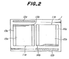
- Fig. 2 is a schematic plan view showing an embodiment of the optical card 1.
- the optical card 1 includes two record areas 11a and 11b which are aligned in the longitudinal direction of the optical card. In case of using the optical card, the card is inserted into the card reader from right or left side.
- the optical card 1 further comprises two position detecting marks 12a, and 12b each corresponding to respective record areas 11as and 11b.
- In each record areas 11a, 11b there are formed a number of data tracks, said tracks extending in the direction in which the card is inserted into the card reader.
- seek portions 13a, 13b and 14a, 14b in which track numbers are recorded, so that data areas 15a, 15b are provided between the seek portions.
- Fig. 3 is a schematic plan view showing the construction of the track 16 in the record 11a.
- the track 16 includes twenty lines which are arranged in parallel with each other in the longitudinal direction of the card and are separated from each other by a constant distance.
- a tenth line counted from the uppermost line there is formed a clock pattern 17 which extends throughout the seek portion 13a, data portion 15a and seek portion 13b.
- the clock pattern 17 is consisting of an array ofg square black blocks arranged equidistantly. By reproducing the clock pattern 17 it is possible to effect the generation of clock pulses and the detection of the focusing and tracking errors. Lines Nos.
- 1, 3 ⁇ 5 and 15 ⁇ 19 in the seek areas 13a, 13b constitute a track number portion 18 in which a track number pattern representing a track number of a relevant track is recorded.
- Lines Nos. 2, 6 ⁇ 8, 12 ⁇ 14 and 20 constitute a track number pattern identifying portion 19 in which an identification pattern for identifying the track number pattern is recorded.
- the track number identification pattern is common for all tracks.
- the track number identifying pattern 19 is formed by the lines Nos. 2, 8, 12 and 10 made of white liens (corresponding to "1" of binary data) and the lines Nos. 6, 7, 13 and 14 made of black lines (corresponding to "0" of binary data).
- the track number written in the track number portion 18 is read out. It should be noted that the track number identifying pattern is existent in a single track and could never be found over two adjacent tracks.
- a plurality of frames 20 are provided in each single track 16, and frame numbers 21 for identifying respective frames are recorded between successive frames 20 as well as between the seek portions 13a, 13b and the frames 20.
- frame numbers 21 for identifying respective frames are recorded between successive frames 20 as well as between the seek portions 13a, 13b and the frames 20.
- a frame synchronizing line 22 in the last line No. 20 so as to derive a frame synchronous signal.
- data signals of two bytes each being composed of eight bits are recorded in upper eight lines Nos. 1 ⁇ 8 and lower eight lines Nos. 12 ⁇ 19. these two byte data signals are read out simultaneously in synchronism with the black clock pattern 17.
- the other record area 13b has the same track construction as that just explained above.
- the seek portion 13a, 13b is read out by moving the optical pick-up in the direction perpendicular to the track direction of the optical card 1 to find a desired track. After the desired track has been found, the information stored in the data portion 15a is read out by moving the optical card 1 in the track direction.
- Fig. 4 is a plan view illustrating an embodiment of the photodetector 8 shown in Fig. 1 for reading the information from the optical card 1 having the track formation illustrated in Fig. 3.
- the photodetector 8 includes eighteen light receiving elements 25- ⁇ 25-17 aligned in the width direction of the track, each of said light receiving elements being corresponded to respective data track lines Nos. 1 ⁇ 8 and 12 ⁇ 20.
- the photodetector 8 further comprises four pairs of clock generating light receiving elements 26-1 ⁇ 26-8 which are arranged to be symmetrical with respect to the line along which the light receiving elements 25-1 ⁇ 25-17 are arranged, and two pairs of focusing and tracking light receiving elements 27-1 ⁇ 27-4 which are arranged also to be symmetrical with respect to the line along which the elements 25-1 ⁇ 25-17 are aligned and are separated from each other in the direction of track width.
- Each of light receiving elements 27-1 ⁇ 27-4 is extended in the track direction such that it receives images of a plurality of clock blocks.
- the optical pick-up is moved in the direction of track width above one of the seek portions 13a, 13b, 14a and 14b, while output signals from the light receiving elements 25-1 ⁇ 25-17 are detected.
- the light receiving elements 25-2, 25-6 ⁇ 25-11 and 25-17 simultaneously detect the black block images, it is certified that the track number identification pattern is detected.
- a track number is detected by processing the output signals from the light receiving elements 25-1, 25-3 ⁇ 25-5, 25-12 ⁇ 25-15 and 25-16. As explained above, only one track number identification pattern is existent in each track 16 and could not be found over two tracks, so that the track number can be read out positively and accurately.
- the optical card 1 When the data stored in the data area 15a, 15b is to be read out, the optical card 1 is moved in the track direction. During this movement, a clock signal is derived from a difference between a sum of output signals from the light receiving elements 26-1, 26-3, 26-5 and 26-7 and a sum of output signals from the light receiving elements 26-2, 26-4, 26-6 and 26-8. In synchronism with the thus derived clock signal, a tracking error signal is derived from a difference between a sum of output signals from the light receiving elements 27-1, 27-3 and a sum of output signals from the light receiving elements 27-2, 27-4. By means of the thus derived tracking error signal, the tracking servo control is effected such that the reading light spot follows the track correctly.
- a focusing error signal is derived from a difference between a sum of output signals from the light receiving elements 26-1 ⁇ 26-8 and a sum of output signals from the light receiving elements 27-1 ⁇ 27-4.
- the focus servo control is carried out to move the objective lens 6 in the optical axis direction such that the focal point 6a of the objective lens 6 is always remained on the optical card 1.
- the data is recovered from the output signals of the light receiving elements 25-1 ⁇ 25-16.
- the semiconductor laser diode 2 is secured to the lens holder 9 such that a longer axis of an elliptical cross section of the laser beam emitted from the laser diode is aligned in the direction of the track width on the optical card 1 and further a light emitting point 2a of the semiconductor laser diode 2 is situated toward the collimator lens 3 with respect to the focal point 3a of the collimator lens 3.
- the stop 4 is so secured to the lens holder 9 that the stop shields partially portions corresponding to the light receiving elements 27-1, 27-2 and 27-3, 27-4 viewed in a shorter axis of the elliptical cross section of the laser beam.
- the light beam emanating from the collimator lens 3 diverges to a small extend and is focused by the objective lens 6 at a position which is far from the objective lens with respect to a focal point 6a of objective lens 6. That is to say, according to the invention, the reading light beam is projected onto the optical card 1 in the de-focused condition and an area of the light spot on the card is sufficiently wide for illuminating a single track viewed in the width direction of the track.
- Figs. 5A, 5B and 5C show the condition of the spot image received by the photodetector 8 at various focus conditions.
- elliptical loci P represent portions which have the same luminance intensity as that at a front edges of light shielded portions 4a, 4a corresponding to the stop 4.
- Fig. 5A illustrates the in-focused condition in which the focal point 6a of the objective lens 6 is just situated on the optical card 1.
- the optical card 1 is moved downward in Fig. 1 and the optical card 1 is situated away from the focal point 6a of the objective lens 6 (forward defocus)
- the illuminated area becomes smaller as shown in Fig. 5B, but when the optical card 1 is moved upward in Fig.
- the area illuminated with the reading light beam becomes larger as illustrated in Fig. 5C. Therefore, when it is set that the difference between the sum of output signals of elements 26-1 ⁇ 26-8 and the sum of output signals of elements 27-1- ⁇ 27-4 becomes zero under the in-focused conditions shown in Fig. 5A, it is possible to derive the focusing error signal which has opposite polarities in the de-focused conditions depicted in Figs. 5B and 5C. Therefore, the focusing servo control is effected such that the focusing error signal is kept zero, and the focused image of the optical card 1 can be always detected.
- the objective lens 1 When the optical card 1 is moved downward in Fig. 1 to a great extent, the illuminated area becomes larger and the polarity of the focusing error signal is reversed, and then the objective lens 1 might be moved upward so that the focusing servo could not be conducted correctly.
- This can be removed by any suitable means. For instance, during the upward movement of the objective lens 6, when the focusing error signal denotes that the objective lens should be moved upward, the objective lens is forcedly moved downward until the polarity of the focusing error signal is reversed.
- the objective lens 6 is driven by an analog signal which is obtained by converting a digital signal supplied from a signal processing circuit such as CPU, when the digital signal exceeds a predetermined threshold value, the objective lens 6 is forcedly moved until the polarity of the focusing error signal is inverted.
- Figs. 6A and 6B are side view and perspective view showing the whole construction of the optical pick-up of the present embodiment.
- the lens holder 9 to which are secured the semiconductor laser diode 2, collimator lens 3, stop 4, beam splitter 5, converging lens 7 and photodetector 8 is fixed to a base 31 made of magnetic material.
- the holder 10 which holds the objective lens 6 is supported by means of four resilient wires 32 movably in the optical axis direction (focusing direction) of the objective lens 6 as well as in the direction (tracking direction) perpendicular both to the focusing direction and the track direction.
- the other ends of wires are secured to a supporting member 33 secured to the base 31.
- a focusing coil 34 which serves to generate a force for moving the holder 10 in the focusing direction.
- tracking coils 35 which generate a force for moving the holder 10 in the tracking direction.
- the tracking coils 35 are formed by a print coil printed on a flexible substrate 36.
- conductive lands for making the connection to the focusing coils 34 and conductive lands for connecting the ends of wires 32 which are also used as electric conductors for the focusing and tracking coils 34 and 35.
- yokes 37 which are introduced into the focusing coils 34, and permanent magnets 38 are secured to the yokes 37 to produce magnetic fluxes which pass through the focusing and tracking coils 34 and 35.
- a projection 31a is formed in the base 31 and a leaf spring 42 is secured to the projection 31a by means of a pin 41. Between the projection 31a and the leaf spring 42 is clamped a guide member 43 which is extended in the track width direction, so that the base 31 can move along the guide member 43. At the other end of the base 31 there are provided projections 31b and 31c which project over and under a lead screw 44 arranged rotatably and extended in the track width direction. To the projection 31b is secured a leaf spring 47 with the aid of a screw 45, and pins 47 are fixed to the leaf spring 46 at its both ends such that tips of these pins are clamped in a groove of the lead screw 44.
- a lubricant sheet 48 so that the base can be easily moved along the lead screw.
- the lead screw 44 is coupled with an output shaft of a motor 50 via worm gears 49. By driving the motor 50 to rotate the lead screw 44 in both directions, the optical pick-up can be moved reciprocally in the direction of the width of the tracks on the optical card 1.
- the information is read out of the optical card, but the present invention may be equally applied to any optical recording mediums other than the optical card by constructing the photodetector in accordance with the track construction.
- the track is formed by a single array of pits as shown in Fig. 8.
- the reading light beam 53 emitted from the semiconductor laser diode and having the elliptical cross section is projected onto the optical disc in the de-focused condition such that the longer axis of the elliptical cross section is aligned in the track direction.
- a photodetector 52 comprises two light receiving elements 54-1,54-2 for receiving an image of a track, two tracking light receiving elements 55-1, 55-2 which are extended in the track direction such that they receive images of opposite side edges of a track adjacent to the relevant track, and three focusing light receiving elements 56-1 ⁇ 56-3 which are aligned in the track direction between successive tracks.
- the information is read out by processing output signals from the light receiving elements 54-1, 54-2, the tracking error signal is derived from a difference between output signals of the light receiving elements 55-1 and 55-2, and the focusing error signal is derived from a difference between a sum of output signals of light receiving elements 56-1 and 56-3 and the output signal of the light receiving element 56-2.
- the tracking error signal is derived from a difference between output signals of the light receiving elements 55-1 and 55-2
- the focusing error signal is derived from a difference between a sum of output signals of light receiving elements 56-1 and 56-3 and the output signal of the light receiving element 56-2.
- the reading light beam emitted from the laser diode 2 is transmitted through the beam splitter 5 and the light reflected by the optical card 1 is reflected by the beam splitter toward the photodetector 8.
- the position of the semiconductor laser diode 2 and collimator lens 3 may be changed by the position of the converging lens 9 and photodetector 8. Then the reading light beam emitted by the laser diode 2 is reflected by the beam splitter 5 toward the optical card and the light reflected by the optical card is transmitted through the beam splitter toward the photodetector 8.
- the beam splitter 5 may be formed by a polarizing beam splitter.
- the light may be used effectively, while the back talk of the laser beam reflected by the optical card onto the semiconductor laser diode can be efficiently prevented.
- the stop 4 may be arranged at any position on the optical path, and as a case may be, the stop may be deleted.
- the light source is formed by the semiconductor laser diode which emits the laser beam having the elliptical cross section. It should be noted that the light beam having a circular cross section may be also used. In this case, the light beam emitted from the semiconductor laser diode may be shpaed into the circular beam by means of a prism. Further, the light source may be formed by light emitting devices other than the semiconductor laser diode.
- the reading light beam is defocused on the optical card 1 by providing the semiconductor laser diode 2 such that its light emitting point 2a is situated near the collimator lens 3 with respect to the focal point 3a thereof.
- the optical record medium is formed such that the record layer is covered with a transparent protection layer. Then, it has been found that even if the reading light beam is projected on the optical record medium such that a size of the beam spot formed on the record layer might be larger than a size of the beam spot formed by light reflected by the record layer on the surface of the transparent layer. Then, the light beam reflected by the record layer is influenced to a great extent by stains and debrises on the surface of transparent layer, and the information could not be read out accurately. According to another aspect of the invention, the above problem can be solved in a sophisticated manner which will be explained hereinafter.
- FIG. 9 is a schematic view showing another embodiment of the optical reading apparatus according to the invention.
- An optical card 61 includes a record layer 61a and a transparent layer 61b applied on the record layer.
- a diffusion plate 62 Between the collimator lens 3 and beam splitter 5 is arranged a diffusion plate 62, and the stop 4 is arranged below the objective lens 6.
- the diffusion plate 62 is formed by a plane glass plate 62a having a number of concave spherical surfaces 62b formed in one surface thereof.
- the optical card 61 has substantially the same track construction as that shown in Fig 3, but the frame line 22 is deleted, so that each track comprises nineteen lines instead of twenty lines.
- the width of a single line is set to 10 ⁇ m
- the width of a single track 16 amounts to 190 ⁇ m
- the width of a single line is designed to be 4 ⁇ m
- the width of a single track is 76 ⁇ m.
- the semiconductor laser diode 2 is arranged such that its light emitting point 2a is shifted with respect to the focal point 3a of the collimator lens 3, so that the reading light beam is projected on the optical card 61 in the de-focused condition.
- the reading light beam is de-focused to such an extent that a focus point F of light rays reflected by the record layer 61a is situated above a middle point M of the transparent layer 61b as shown in Fig. 11A, a size of a spot S2 formed on the surface of transparent layer 61b by light reflected by the record layer 61a becomes smaller than that of a spot S1 formed on the record layer 61a.
- the de-focus amount is so set that the focus point F of the light rays reflected from the record layer 61a becomes lower than the middle point M of the transparent layer 61b as shown in Fig. 11B.
- the spot S2 formed on the surface of transparent layer 61b has a larger area than the spot S1 on the record layer 61a, and therefore the information can be read out accurately without being influenced by the stains or debrises on the surface of transparent layer 61b.
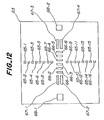
- Fig. 12 is a plan view depicting the construction of a photodetector 63 in the present embodiment.
- the photodetector 63 comprises light receiving elements 65-1 ⁇ 65-16 aligned in the track width direction, each elements being corresponded to respective one of sixteen tracks.
- the photodetector 63 further comprises three pairs of light receiving elements 66-1 ⁇ 66-6 which are arranged symmetrically with the array of the elements 65-1 ⁇ 65-16 and are separated from each other by a distance corresponding to the distance of the blocks of the clock line 17 (see (Fig.
- Fig. 13 illustrates the positional relationship between the image of the illuminated portion of the optical card 61 and the light receiving elements of the photodetector 63.
- the stop 4 is so formed that the shielded portion 4a is partially positioned on the light receiving elements 67-1 ⁇ 67-4 viewed in the direction of the short axis of the elliptical cross section of the light beams.
- Fig. 14 is a circuit diagram showing an embodiment of the signal processing circuit for deriving the data signal and control signals such as the clock signal, focusing and tracking error signals, and track number signal.
- the optical pick-up is moved above the seek portion 13a, 13b, 14a, 14b in the direction of the width of the track on the optical card 61, and the output signals from the light receiving elements 65-1 ⁇ 65-16 are monitored by a reading circuit 70.
- the reading circuit 70 detects the track number identification pattern, a track number is read out.
- the seek operation is ended when a desired track number has been detected.
- the optical card 61 is moved in the track direction to read out the data stored in the data area 15a, 15b.
- a first sum of output signals of the light receiving elements 66-1, 66-3, 66-5 is derived by an adder 71-1 and a second sum of output signals of the light receiving elements 76-2, 76-4, 76-6 is obtained by an adder 71-2. Then a difference between the first and second sums is derived by a substracter 72-1 to produce the clock signal CK.
- a third sum of output signals of the light receiving elements 67-1, 67-3 and a fourth sum of output signals of the elements 67-2, 67-4 are derived by adders 71-3 and 71-4, respectively. Then, a difference between the third and fourth sums is derived by a subtracter 72-2 to generate the tracking error signal TE.
- the tracking error signal TE is supplied to a tracking driver circuit 73 and the tracking servo control is effected under the control of the clock signal CK.
- a fifth sum of output signals of the light receiving elements 66-1 ⁇ 66-6 is formed by an adder 71-5 and a sixth sum of output signals of the elements 67-1 ⁇ 67-4 is derived by an adder 71-6.
- a difference between the fifth and sixth sums is derived by a subtracter 72-3 to produce the focusing error signal FE.
- the focusing error signal FE is supplied to a focusing driver circuit 74 to effect the focusing servo control under the control of the clock signal CK.
- the data signal can be derived by processing the output signals of the light receiving elements 65-1 ⁇ 6516 under the control of the clock signal CK.
- Output signals of the light receiving elements 68-1 and 68-2 are supplied to abnormality detecting circuits 75-1 and 75-2, respectively, whose output signals are supplied to the tracking and focusing driver circuits 73 and 74, respectively.
- Fig. 15 shows a situation that a defect D is existent in the clock pattern 17.
- the defect is first detected by the element 68-2.
- the output signal of the element 68-2 becomes higher than a predetermined value which will be obtained when a normal clock pattern is detected by the element 68-2, but when the defect F has a lower reflectivity and has a larger area than the normal clock pattern, the output signal becomes lower than the predetermined value.
- the aperture of the elements 68-1, 68-2 is made slightly larger than the image of a single clock pattern.
- the defect D is first detected by the light receiving element 68-1.
- the output signals of the elements 68-1, 68-2 are compared with a threshold value corresponding to the predetermined value to identify that the defect D is existent in the clock pattern line 17.
- the focusing and tracking servo loops are locked.
- the same defect D is detected by the elements 68-1 or 68-2 situating at a downstream position viewed in the moving direction of the optical card, the focusing and tracking servo loops are unlocked. In this manner, the information can be read out correctly without being influenced by the defect D in the clock pattern line 17.
- the image of defect D is received by, for example the light receiving elements 67-3, 67-4 so that the amplitude of the focusing and tracking error signals becomes large. Then the objective lens 6 might be moved in the optical axis direction to a large extent and the light spot might deviate from the track, so that the information could not be read out correctly.
- the defect D is detected by the light emitting elements 68-1, 68-2 provided outside the focusing and tracking error detecting region and the focusing and tracking servo controls are locked, so that the information can be always read out accurately.
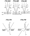
- Figs. 16A to 16C show various focus conditions.
- Fig. 16A illustrates the in-focused condition in which the focal point of the objective lens 6 is situated on the record layer 61a.
- the optical card 61 is moved downward, the size of the illuminated portion of the record layer 61a becomes smaller as illustrated in Fig. 16B, and when the optical card is moved upward, the size of the illuminated portion becomes larger as depicted in Fig. 16C. Therefore, when the apparatus is so set that the difference between the sums of elements 26-1 ⁇ 26-6 and 27-1 ⁇ 27-4, i.e. the output signal from the subtracter 72-3 in Fig.
- the objective lens 6 can be always remained in the in-focused condition with respect to the record layer 61a of the optical disc 61.
- the stop 4 is not provided, when the optical card is moved away from the objective lens 6 (backward defocus), the area of the portion on the optical card illuminated by the reading light becomes larger, and the polarity of the focusing error signal is inverted as illustrated in Fig. 17A and the objective lens 6 is driven by the focus servo control in the direction separating from the optical card and the backward defocus is enhanced. Therefore, an effective focus servo range is reduced.
- the stop 4 is arranged between the objective lens 6 and the optical card 61, when the backward de-focused condition is manifested, the outer periphery light rays are shielded by the stop 4, so that the focus servo range can be increased as shown in Fig. 17B.
- the diffusion plate 62 is provided between the laser diode 2 and the beam splitter 5, but the diffusion plate may be deleted or may be replaced by other light diffusing plate such as translucent glass plate. Further the diffusion plate may be formed in various ways as shown in Figs. 18A to 18C.
- a diffusion plate 75 has a transparent portion 75a whose contour corresponds to the region of the light receiving elements of the photodetector 63 and a light diffusing portion 75b.
- a plate 76 has a central portion 75a having a higher transmittivity than a peripheral portion 75b.
- the contour configuration of the central portion 75a corresponds to the region of the light receiving elements.
- the transmittivity T of a plate 77 is continuously changed. That is to say, a central portion 77a has a higher transmittivity than a peripheral portion 77b.
- the stop 4 may be provided between the collimator lens 3 and the beam splitter 5, or between the beam splitter 5 and the objective lens 6 or between the beam splitter 5 and the converging lens 8. Further, the stop 4 may be deleted.
- the focusing and tracking servo loops are locked. Instead of locking the servo loops, it is also possible to decrease the gain of the servo loops upon the detection of the defect.
- the optical card is read only in a single direction, it is sufficient to provide only one light receiving element for detecting the defect. Further, only one of the tracking and focusing servo may be controlled by the detection of the defect.
- a pulse generator may be actuated in response to the detection of the defect by the abnormality detecting circuits 75-1 or 75-2 to generate a clock signal for a time period during which the defect image D passes through the photodetector 63.
- Fig. 19 is a schematic view illustrating still another embodiment of the optical reading apparatus according to the invention. Also, in the present embodiment, portions similar to those shown in the previous embodiments are denoted by the same reference numerals used in the previous embodiments.
- the light source is constituted by a light emitting diode 81 whose light emitting point 81a is arranged to be near the collimator lens 3 with respect to the focal point 3a of the collimator lens, so that the reading light beam is projected onto the optical card 1 in the defocused condition, so that a large area on the optical card 1 can be illuminated.
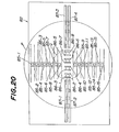
- Fig. 20 is a schematic plan view showing the construction of a photodetector 82 having a similar construction to that shown in Fig. 4.
- sixteen light receiving elements 85-1 ⁇ 85-16 for detecting the data
- four pairs of light receiving elements 86-1 ⁇ 86-8 for generating the clock signal and focusing error signal
- two pairs of light receiving elements 87-1 ⁇ 87-4 for deriving the focusing and tracking errors.
- the light receiving elements 87-1 ⁇ 87-4 are extended in the track direction such that a plurality of clock blocks in the clock pattern line are simultaneously detected.
- the size of the image P of the illuminated portion of the optical card is changed. Therefore, by deriving a difference between a sum of output signals of light receiving elements 86-1 ⁇ 86-8 and a sum of output signals of elements 87-1, 87-2, and a difference between a sum of output signals of the elements 86-1 ⁇ 86-8 and a sum of output signals of elements 87-3, 87-4, there are obtained two focusing error signals FE1 and FE2. Similarly, when the optical card is shifted in the direction perpendicular to the track direction, the image P of the illuminated portion is also shifted in up and down direction.
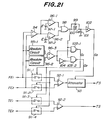
- Fig. 21 is a circuit diagram showing a circuit for deriving the focusing servo signal and the tracking servo signal from the above mentioned focusing and tracking error signals FE1, FE2, TE1 and TE2.
- the focusing error signals FE1 and FE2 are suppled via switches 91-1 and 91-2, respectively to an adder 92-1 whose output signal is supplied to an attenuator 93 to derive a focus servo signal FS.
- the tracking error signals TE1 and TE2 are supplied via switches 91-3 and 91-4, respectively to an adder 92-2 to derive a tracking servo signal TS.
- the focusing error signals FE1 and FE2 are further supplied to a subtracter 94 to derive a difference therebetween and also to absolute value circuits 95-1 and 95-2.
- absolute value circuits 95-1, 95-2 absolute values of differences between the focusing error signals FE1 and FE2 and a reference level are detected.
- the output signal of the subtracter 94 is supplied to one input terminals of comparators 96-1 and 96-2.
- comparators 96-1, 96-2 To the other input terminals of the comparators 96-1, 96-2 are applied reference voltages +E and -E, respectively from reference voltage sources 97-1 and 97-2, respectively.
- the output signal of the subtracter 94 is compared with the reference voltages +E, -E, and when the output signal exceeds +E or is lower than -E, an OR gate 98 generates an output signal of a logic high level (H).
- the comparators 96-1, 96-2 and OR gate 98 form a so-called window comparator.
- the output signal of the OR gate 98 is supplied via diode 99, resistor 100 and capacitor 101 to a buffer 102 of the Schmitt input.
- the buffer 102 supplies a control signal G3 to the attenuator 93, said control signal being extended or prolonged by a time constant determined by a resistance value Rd of the resistor 100 and a capacitance value Cd of the capacitor 101 only when the output of the OR gate 98 is in the high level.
- the output of the adder 92-1 is attenuated in the attenuator 93.
- the attenuator 93 does not attenuate the signal, and the output of the adder 92-1 is supplied as the focus servo signal FS.
- the output signals of the absolute value circuits 95-1, 95-2 are compared with each other in a comparator 96-3.
- the output signal of the comparator 96-3 is supplied to one input of NAND gate 103-1 directly as well as to one input of NAND gate 103-2 via an inverter 104.
- To the other inputs of the NAND gates 103-1, 103-2 is supplied the output signal of the OR gate 98.
- the NAND gate 103-1 generates a control signal G1 which controls the switches 91-1 and 91-3 in such a manner that only when the output of the NAND gate 103-1 is in H level, the switches 91-1 and 91-3 are made on.
- the NAND gate 103-2 produces a control signal G2 which serves to control the switches 91-2 and 91-4. When the control signal G2 is in the H level, the switches 91-2, 91-4 are made on, but when the control signal G2 has the L level, these switches are made off.
- the focusing error signals FE1 and FE2 have substantially the same amplitude and the output of the subtracter 93 is in a range from -E to +E. Therefore, the output of the OR gate 98 is in the L level, so that the control signals G1 and G2 are in the H level in regardless of the output of the comparator 96-3, and thus all the switches 91-1 ⁇ 91-4 are made on. Further, when the control signal G3 is in the L level, the attenuator 93 does not effect the attenuation and the output signal of the adder 92-1 is passed through the attenuator without being attenuated. Therefore, the focusing servo signal FS becomes a sum of the focusing error signals FE1 and FE2 and the tracking servo signal TS becomes a sum of the tracking error signals TE1 and TE2.
- the image of defect D is moved in the track direction with respect to the photodetector 82 as shown in Figs. 22A ⁇ 22E.
- the light receiving elements 85-1 ⁇ 85-16 are omitted for the sake of simplicity.
- the output of the subtracter 94 is increased or decreased.
- the output of the OR gate 98 is changed into the H level.
- This high level output of the OR gate 98 is supplied to the buffer 102 via the diode 99 and the control signal G3 becomes high level, so that the attenuator 93 effects the attenuation.
- the defect D affects the focusing error signal FE2
- the output of the absolute value detecting circuit 95-2 becomes larger than that of the circuit 95-1, so that the output of the comparator 96-3 becomes low level. Therefore, the control signals G1 and G2 become H and L levels, respectively, and the switches 91-2, 91-3 are made on, but the switches 91-2, 91-4 are made off.
- the focusing error signal FE2 and tracking error signal TE2 are cut, and the focus servo signal FS is formed by the focusing error signa FE1 attenuated by the attenuator 93 and the tracking servo signal TS is constituted solely by the tracking error signal TE1.
- the output of the comparator 96-3 becomes high level, so that the control signals G1 and G2 become low and high levels, respectively. Therefore, the switches 91-1, 91-3 are made off and the switches 91-2, 91-4 are made on.
- the focusing and tracking error signals FE1 and TE1 are cut off, and the tracking servo signal TS is formed by the tracking error signal TE2 and the focusing servo signal FS is made by the focusing error signal FE2 attenuated by the attenuator 93.
- the focusing error signals FE1 and FE2 are influenced by the defect to the substantially same extent, so that the output of the OR gate 98 becomes low and all the switches 91-1 ⁇ 91-4 are made on.
- the defect is detected by the elements 87-3, 87-4 or 87-1, 87-2 depending upon the direction of the movement of the optical card. At that time, the difference between the focusing error signals FE1 and FE2 becomes large and the output of the OR gate 98 becomes high.
- This output signal of high level is delayed by the delaying function of the resistor 100 and capacitor 101, so that the output of the buffer 102, i.e. the control signal G3 is remained high for a predetermined period which is set to be a loner than a time period during which the defect affects the elements 86-1 ⁇ 86-8. In this manner, even when both the focusing error signals FE1 and FE2 are simultaneously influenced by the defect, the influence can be mitigated and the servo control can be affected accurately.
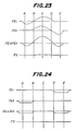
- Figs. 23 and 24 show the variation of the various signals appearing at various points in the circuit shown in Fig. 21 at various timings A ⁇ E which correspond to the situations shown in Figs. 22A ⁇ 22E, respectively.
- the focusing error signal is detected by utilizing the fact that the size of image of the light beam projected upon the photodetector is changed in accordance with the de-focused condition.
- the focusing error could be detected by any other means.
- the focusing error signal may be derived by utilizing the fact that the light beam includes a circular or elliptical ring portion at which the luminous intensity is not changed in regardless of the focus condition.
- the above explained ring portion is represented by a dotted circle Q.
- the focusing error signal may be obtained by deriving a difference between a sum of output signals of light receiving elements 86-1 ⁇ 86-8 and a sum of output signals of light receiving elements 87-1 ⁇ 87-4. In this manner, the focus condition can be detected accurately with a high sensitivity in the differential manner.
- the other focusing or tracking error signal is exclusively used to derive the focusing or tracking servo signal, so that the information can be read out always correctly.
Landscapes
- Physics & Mathematics (AREA)
- Optics & Photonics (AREA)
- Optical Recording Or Reproduction (AREA)
- Optical Head (AREA)
Applications Claiming Priority (8)
| Application Number | Priority Date | Filing Date | Title |
|---|---|---|---|
| JP63012489A JP2856356B2 (ja) | 1988-01-25 | 1988-01-25 | 光学式情報読み取り装置 |
| JP12489/88 | 1988-01-25 | ||
| JP46028/88 | 1988-02-29 | ||
| JP63046028A JP2746593B2 (ja) | 1988-02-29 | 1988-02-29 | 光学式情報読み取り装置 |
| JP54750/88 | 1988-03-10 | ||
| JP5475088A JPH01229432A (ja) | 1988-03-10 | 1988-03-10 | 光学式情報読み取り装置 |
| JP12045688A JPH01292629A (ja) | 1988-05-19 | 1988-05-19 | 光学式情報読み取り装置 |
| JP120456/88 | 1988-05-19 |
Publications (3)
| Publication Number | Publication Date |
|---|---|
| EP0326354A2 true EP0326354A2 (fr) | 1989-08-02 |
| EP0326354A3 EP0326354A3 (fr) | 1991-04-17 |
| EP0326354B1 EP0326354B1 (fr) | 1995-05-24 |
Family
ID=27455816
Family Applications (1)
| Application Number | Title | Priority Date | Filing Date |
|---|---|---|---|
| EP89300699A Expired - Lifetime EP0326354B1 (fr) | 1988-01-25 | 1989-01-25 | Appareil de lecture d'information sur un support d'enregistrement optique |
Country Status (3)
| Country | Link |
|---|---|
| US (1) | US5155718A (fr) |
| EP (1) | EP0326354B1 (fr) |
| DE (1) | DE68922756T2 (fr) |
Cited By (5)
| Publication number | Priority date | Publication date | Assignee | Title |
|---|---|---|---|---|
| EP0441435A1 (fr) * | 1990-02-06 | 1991-08-14 | Koninklijke Philips Electronics N.V. | Dispositif de balayage optique à plusieurs spots de balayage |
| EP0415518A3 (en) * | 1989-08-28 | 1991-11-13 | Pioneer Electronic Corporation | Signal recording apparatus and signal reproducing apparatus |
| EP0523319A1 (fr) * | 1991-07-19 | 1993-01-20 | Pioneer Electronic Corporation | Dispositif de photo-detection |
| WO2007054905A1 (fr) * | 2005-11-14 | 2007-05-18 | Koninklijke Philips Electronics N.V. | Procede et systeme pour regler le pas de spots lumineux servant a la lecture d'un support d'information |
| CN102622570A (zh) * | 2010-12-30 | 2012-08-01 | 霍尼韦尔国际公司 | 条形码成像器 |
Families Citing this family (15)
| Publication number | Priority date | Publication date | Assignee | Title |
|---|---|---|---|---|
| EP0588385B1 (fr) * | 1989-02-13 | 1997-10-15 | Omron Corporation | Appareil d'enregistrement/réproduction de données pour carte optique |
| JP2569957B2 (ja) * | 1990-12-05 | 1997-01-08 | ティアック株式会社 | ヘッドキャリッジ駆動装置 |
| US5412636A (en) * | 1991-03-22 | 1995-05-02 | Olympus Optical Co., Ltd. | Apparatus for servo-controlling objective lens in recording and/or reproducing apparatus using optical record medium |
| JPH04356729A (ja) * | 1991-03-28 | 1992-12-10 | Olympus Optical Co Ltd | 光学的情報記録再生装置 |
| US5206852A (en) * | 1991-06-29 | 1993-04-27 | Samsung Electronics Co., Ltd. | High-density recording optical head |
| JPH05128554A (ja) * | 1991-11-01 | 1993-05-25 | Olympus Optical Co Ltd | 光学的情報記録再生装置 |
| JPH05128536A (ja) * | 1991-11-01 | 1993-05-25 | Olympus Optical Co Ltd | 光記録媒体の再生装置 |
| US5425012A (en) * | 1992-06-01 | 1995-06-13 | Olympus Optical Co., Ltd. | Track detector circuit for detecting a track when at least either optical recording or regenaration is performed on a card-like information recording medium |
| JPH0689446A (ja) * | 1992-09-07 | 1994-03-29 | Olympus Optical Co Ltd | 光学的情報記録再生装置及びトラックジャンプ方法 |
| JP3736812B2 (ja) * | 1994-06-13 | 2006-01-18 | パイオニア株式会社 | 光学式ピックアップ装置 |
| JPH09115161A (ja) * | 1995-10-18 | 1997-05-02 | Nec Corp | 光学ヘッド装置 |
| AU7570896A (en) * | 1995-11-15 | 1997-06-05 | Zen Research N.V. | Track detection methods and apparatus for simultaneous electronic monitoring of multiple adjacent tracks of an optical disk |
| US5780829A (en) * | 1997-01-31 | 1998-07-14 | Mustek Systems Inc. | Flat-plate scanner having a beam-splitting prism/mirror and two light emitting sources |
| US6229771B1 (en) | 1998-10-09 | 2001-05-08 | Zen Research (Ireland), Ltd. | Method and apparatus for generating focus error signals in a multi-beam optical disk drive |
| CN105570819A (zh) * | 2014-10-15 | 2016-05-11 | 富泰华工业(深圳)有限公司 | 背光源 |
Family Cites Families (15)
| Publication number | Priority date | Publication date | Assignee | Title |
|---|---|---|---|---|
| JPS55163635A (en) * | 1979-06-04 | 1980-12-19 | Mitsubishi Electric Corp | Optical tracking device |
| JPS5683849A (en) * | 1979-12-11 | 1981-07-08 | Matsushita Electric Ind Co Ltd | Optical information reader |
| JPS57208647A (en) * | 1981-06-18 | 1982-12-21 | Toshiba Corp | Optical disk for recording of information |
| US4805162A (en) * | 1982-11-01 | 1989-02-14 | Storage Technology Partners Ii | Fine and coarse servo system for access and tracking on an optical disk |
| US4661942A (en) * | 1983-08-26 | 1987-04-28 | Mitsubishi Denki Kabushiki Kaisha | Control apparatus for information storage and retrieval system |
| JPS618744A (ja) * | 1984-06-22 | 1986-01-16 | Fuji Photo Film Co Ltd | 光デイスク装置のフオ−カス誤差検出装置 |
| JPS6118918A (ja) * | 1984-07-05 | 1986-01-27 | Ricoh Co Ltd | ビ−ム整形光学系 |
| US4626671A (en) * | 1984-07-06 | 1986-12-02 | Honeywell Information Systems Inc. | Lens system for optically recorded storage card reader |
| US4787075A (en) * | 1984-12-26 | 1988-11-22 | Canon Kabushiki Kaisha | Optical information recording medium and apparatus for recording/reproducing information using the same |
| JPS61153834A (ja) * | 1984-12-27 | 1986-07-12 | Canon Inc | 光学的情報記録再生装置 |
| JPS62279523A (ja) * | 1986-05-28 | 1987-12-04 | Olympus Optical Co Ltd | 光カ−ドのデ−タ読取方法 |
| US4918415A (en) * | 1986-05-23 | 1990-04-17 | Olympus Optical Co., Ltd. | Data reading and/or writing apparatus for use with an optical card |
| US4730293A (en) * | 1986-09-15 | 1988-03-08 | Drexler Technology Corporation | Dual beam optical data system |
| US4918675A (en) * | 1986-12-04 | 1990-04-17 | Pencom International Corporation | Magneto-optical head with separate optical paths for error and data detection |
| JPH01105338A (ja) * | 1987-07-14 | 1989-04-21 | Mitsubishi Electric Corp | 光記録再生装置 |
-
1989
- 1989-01-23 US US07/299,530 patent/US5155718A/en not_active Expired - Fee Related
- 1989-01-25 EP EP89300699A patent/EP0326354B1/fr not_active Expired - Lifetime
- 1989-01-25 DE DE68922756T patent/DE68922756T2/de not_active Expired - Fee Related
Cited By (6)
| Publication number | Priority date | Publication date | Assignee | Title |
|---|---|---|---|---|
| EP0415518A3 (en) * | 1989-08-28 | 1991-11-13 | Pioneer Electronic Corporation | Signal recording apparatus and signal reproducing apparatus |
| EP0441435A1 (fr) * | 1990-02-06 | 1991-08-14 | Koninklijke Philips Electronics N.V. | Dispositif de balayage optique à plusieurs spots de balayage |
| EP0523319A1 (fr) * | 1991-07-19 | 1993-01-20 | Pioneer Electronic Corporation | Dispositif de photo-detection |
| US5398228A (en) * | 1991-07-19 | 1995-03-14 | Pioneer Electronic Corporation | Photo-detecting device for reproducing information recorded on an optical disk |
| WO2007054905A1 (fr) * | 2005-11-14 | 2007-05-18 | Koninklijke Philips Electronics N.V. | Procede et systeme pour regler le pas de spots lumineux servant a la lecture d'un support d'information |
| CN102622570A (zh) * | 2010-12-30 | 2012-08-01 | 霍尼韦尔国际公司 | 条形码成像器 |
Also Published As
| Publication number | Publication date |
|---|---|
| DE68922756D1 (de) | 1995-06-29 |
| EP0326354A3 (fr) | 1991-04-17 |
| EP0326354B1 (fr) | 1995-05-24 |
| DE68922756T2 (de) | 1995-09-28 |
| US5155718A (en) | 1992-10-13 |
Similar Documents
| Publication | Publication Date | Title |
|---|---|---|
| US5155718A (en) | Optical record medium reading apparatus having a de-focussed light beam projected on an optical record medium | |
| US4924199A (en) | Optical card for data storage for use in a data recording and retrieving apparatus | |
| CA1067618A (fr) | Appareil de lecture optique par reflexion | |
| US3992574A (en) | Opto-electronic system for determining a deviation between the actual position of a radiation-reflecting plane in an optical imaging system and the desired position of said plane | |
| US4817074A (en) | Method and apparatus for detecting the focusing state and positioning accuracy of a light beam directed onto an optical disk tracking guide in an optical recording system | |
| EP0164687B1 (fr) | Tête optique pour focalisation d'un faisceau de lumière sur un disque optique | |
| GB1502151A (en) | Apparatus for reading a record carrier on which information is stored in a optically readable structure | |
| US5027339A (en) | Optical card analyzing apparatus | |
| EP0260569A2 (fr) | Tête optique | |
| EP0384358B1 (fr) | Système d'enregistrement et de reproduction à double source lumineuse | |
| JPH01116930A (ja) | 光ビーム位置検出装置 | |
| US5157249A (en) | Miniaturized optical pick-up with high sensitivity focusing error detecting device | |
| EP0475523A1 (fr) | Dispositif pour balayer une face d'information à l'aide de rayonnement optique | |
| US5179267A (en) | Data reading and/or writing apparatus of type using optical card | |
| KR100227668B1 (ko) | 검출회로 및 방법 | |
| HK113395A (en) | Optical scanning device | |
| JP2746593B2 (ja) | 光学式情報読み取り装置 | |
| EP0856838B1 (fr) | Procede et dispositif de regulation du suivi d'une carte a memoire optique | |
| JP2716765B2 (ja) | 光学式記録媒体へのデータ記録方法 | |
| EP0568010A1 (fr) | Procédé et appareil pour la lecture de données optiques | |
| JP2730133B2 (ja) | 光カード処理装置 | |
| JPH01303637A (ja) | 光学式情報読み取り装置 | |
| KR930002128Y1 (ko) | 촛점생성과 에러검출을 겸한 광픽업대물렌즈 | |
| JPH0268719A (ja) | 光記録媒体の読取り装置 | |
| JPH08235605A (ja) | 光デイスク装置 |
Legal Events
| Date | Code | Title | Description |
|---|---|---|---|
| PUAI | Public reference made under article 153(3) epc to a published international application that has entered the european phase |
Free format text: ORIGINAL CODE: 0009012 |
|
| AK | Designated contracting states |
Kind code of ref document: A2 Designated state(s): DE GB |
|
| PUAL | Search report despatched |
Free format text: ORIGINAL CODE: 0009013 |
|
| AK | Designated contracting states |
Kind code of ref document: A3 Designated state(s): DE GB |
|
| 17P | Request for examination filed |
Effective date: 19910626 |
|
| 17Q | First examination report despatched |
Effective date: 19930504 |
|
| GRAA | (expected) grant |
Free format text: ORIGINAL CODE: 0009210 |
|
| AK | Designated contracting states |
Kind code of ref document: B1 Designated state(s): DE GB |
|
| REF | Corresponds to: |
Ref document number: 68922756 Country of ref document: DE Date of ref document: 19950629 |
|
| PLBE | No opposition filed within time limit |
Free format text: ORIGINAL CODE: 0009261 |
|
| STAA | Information on the status of an ep patent application or granted ep patent |
Free format text: STATUS: NO OPPOSITION FILED WITHIN TIME LIMIT |
|
| 26N | No opposition filed | ||
| PGFP | Annual fee paid to national office [announced via postgrant information from national office to epo] |
Ref country code: GB Payment date: 19990128 Year of fee payment: 11 |
|
| PGFP | Annual fee paid to national office [announced via postgrant information from national office to epo] |
Ref country code: DE Payment date: 19990201 Year of fee payment: 11 |
|
| PG25 | Lapsed in a contracting state [announced via postgrant information from national office to epo] |
Ref country code: GB Free format text: LAPSE BECAUSE OF NON-PAYMENT OF DUE FEES Effective date: 20000125 |
|
| GBPC | Gb: european patent ceased through non-payment of renewal fee |
Effective date: 20000125 |
|
| PG25 | Lapsed in a contracting state [announced via postgrant information from national office to epo] |
Ref country code: DE Free format text: LAPSE BECAUSE OF NON-PAYMENT OF DUE FEES Effective date: 20001101 |