EP0326883B1 - Bascule non volatile, électriquement modifiable à consommation nulle - Google Patents
Bascule non volatile, électriquement modifiable à consommation nulle Download PDFInfo
- Publication number
- EP0326883B1 EP0326883B1 EP89101040A EP89101040A EP0326883B1 EP 0326883 B1 EP0326883 B1 EP 0326883B1 EP 89101040 A EP89101040 A EP 89101040A EP 89101040 A EP89101040 A EP 89101040A EP 0326883 B1 EP0326883 B1 EP 0326883B1
- Authority
- EP
- European Patent Office
- Prior art keywords
- inverter
- latch
- floating gate
- potential
- gate
- Prior art date
- Legal status (The legal status is an assumption and is not a legal conclusion. Google has not performed a legal analysis and makes no representation as to the accuracy of the status listed.)
- Expired - Lifetime
Links
- 238000007667 floating Methods 0.000 claims description 50
- 239000003990 capacitor Substances 0.000 claims description 14
- 230000008878 coupling Effects 0.000 claims description 14
- 238000010168 coupling process Methods 0.000 claims description 14
- 238000005859 coupling reaction Methods 0.000 claims description 14
- 230000005641 tunneling Effects 0.000 claims description 9
- 230000003068 static effect Effects 0.000 claims description 6
- 230000000295 complement effect Effects 0.000 claims description 5
- 239000007943 implant Substances 0.000 claims description 5
- 230000015654 memory Effects 0.000 description 47
- 230000005684 electric field Effects 0.000 description 11
- 230000005669 field effect Effects 0.000 description 10
- 238000000034 method Methods 0.000 description 5
- 229910021420 polycrystalline silicon Inorganic materials 0.000 description 5
- 238000010586 diagram Methods 0.000 description 4
- 229920005591 polysilicon Polymers 0.000 description 4
- 239000000758 substrate Substances 0.000 description 4
- XUIMIQQOPSSXEZ-UHFFFAOYSA-N Silicon Chemical compound [Si] XUIMIQQOPSSXEZ-UHFFFAOYSA-N 0.000 description 3
- 238000013459 approach Methods 0.000 description 3
- 238000005516 engineering process Methods 0.000 description 3
- 229910052710 silicon Inorganic materials 0.000 description 3
- 239000010703 silicon Substances 0.000 description 3
- 238000003491 array Methods 0.000 description 2
- 230000007423 decrease Effects 0.000 description 2
- 238000004806 packaging method and process Methods 0.000 description 2
- 239000004065 semiconductor Substances 0.000 description 2
- 102100034033 Alpha-adducin Human genes 0.000 description 1
- 101000799076 Homo sapiens Alpha-adducin Proteins 0.000 description 1
- 101000629598 Rattus norvegicus Sterol regulatory element-binding protein 1 Proteins 0.000 description 1
- 230000004888 barrier function Effects 0.000 description 1
- 238000010276 construction Methods 0.000 description 1
- 238000006880 cross-coupling reaction Methods 0.000 description 1
- 229910021419 crystalline silicon Inorganic materials 0.000 description 1
- 230000002950 deficient Effects 0.000 description 1
- 239000003989 dielectric material Substances 0.000 description 1
- 238000009792 diffusion process Methods 0.000 description 1
- 230000006870 function Effects 0.000 description 1
- 230000036039 immunity Effects 0.000 description 1
- 238000002347 injection Methods 0.000 description 1
- 239000007924 injection Substances 0.000 description 1
- 230000014759 maintenance of location Effects 0.000 description 1
- 238000004519 manufacturing process Methods 0.000 description 1
Images


Classifications
-
- G—PHYSICS
- G11—INFORMATION STORAGE
- G11C—STATIC STORES
- G11C14/00—Digital stores characterised by arrangements of cells having volatile and non-volatile storage properties for back-up when the power is down
-
- H—ELECTRICITY
- H03—ELECTRONIC CIRCUITRY
- H03K—PULSE TECHNIQUE
- H03K3/00—Circuits for generating electric pulses; Monostable, bistable or multistable circuits
- H03K3/02—Generators characterised by the type of circuit or by the means used for producing pulses
- H03K3/353—Generators characterised by the type of circuit or by the means used for producing pulses by the use, as active elements, of field-effect transistors with internal or external positive feedback
- H03K3/356—Bistable circuits
- H03K3/356008—Bistable circuits ensuring a predetermined initial state when the supply voltage has been applied; storing the actual state when the supply voltage fails
Definitions
- the present invention relates to an electrically alterable nonvolatile latch element which can be used as a basic element in the construction of electrically reconfigurable logic blocks.
- fusible link technology requires substantial chip area to fabricate the fusible link elements. Also, the programming circuitry required to "blow" the fusible link needs to be large because the link requires a relatively large amount of current to flow through it to "blow” with a certain degree of reliability.
- Another technique known as the laser link technique, utilizes a highly directed laser beam to selectively separate the links in a memory circuit with redundant rows or columns. This technique allows the replacement of a limited number of defective memory locations with the redundant memory locations.
- a disadvantage of this technique is that it requires substantial investment in capital equipment to implement.
- U.S. Pat. No. 4,132,904 discloses a volatile/nonvolatile logic latch circuit with a pair of circuit branches, each comprising a field effect transistor and a floating gate field effect transistor connected in series. The control gates of the floating gate field effect transistors are cross-coupled to the common junctions of the series-connected transistors in the other branch.
- This circuit can be programmed to assume the desired state when power is turned on and can also be intentionally written over if complementary data is to be stored.
- U.S. Pat. No. 4,571,704 discloses a nonvolatile latch circuit which assumes the proper state when power is applied to the circuit, irrespective of the power-applying conditions. This is accomplished by configuring a pair of circuit branches with each branch comprising a field effect transistor connected in series with a floating gate field effect transistor. The gates of the normal field effect transistors are cross-coupled to the common junctions between the series transistors in the other circuit branch. Also, the control gates of the floating gate field effect transistors are capacitively cross-coupled to the floating gates of the transistors in the other branch.
- the latch element of the present invention is defined by independent patent claim 1.
- the invention and the document US-A-4,571,704 mentioned above share the features set forth in the preamble of patent claim 1.
- An electrically programmable latch in accordance with the present invention includes two basic components: a) two nonvolatile memory cell elements and b) one cross-coupled static latch.
- the two nonvolatile memory cell elements are metal-oxide-semiconductor field effect transistor (MOSFET) devices which form the two branches of the circuit module.
- MOSFET metal-oxide-semiconductor field effect transistor
- the floating gates of the nonvolatile memory cell elements in the two branches are capacitively coupled to their respective control gates via coupling capacitors which are formed by the overlap area between the control gate and the floating gate with a thin oxide dielectric separating the floating gates from the control gates.
- the floating gate of one memory cell element in one branch is capacitively coupled to the control gate of the other memory cell element in the other branch and vice-versa.
- This capacitive cross-coupling is achieved via relatively small area tunneling capacitors commonly known to those skilled in the art as Fowler-Nordheim capacitors.
- the drain of the nonvolatile memory cell element in one branch is coupled to the input of a complementary metal-oxide-semiconductor (CMOS) inverter, while the drain of the nonvolatile memory cell element in the other branch is coupled to the input of a second CMOS inverter.
- CMOS complementary metal-oxide-semiconductor
- the output of the first CMOS inverter is coupled to the input of the second CMOS inverter which is also coupled to the drain of the nonvolatile memory element in the second branch.
- the output of the second CMOS inverter is coupled to the input of the first CMOS inverter which is also coupled to the drain of the nonvolatile memory element in the first branch.
- the two cross-coupled CMOS inverters form a configuration which is commonly known to those skilled in the art as a static cross-coupled latch.
- the cross-coupled CMOS inverters are intended to sense the state of the two nonvolatile memory elements in the two branches and present the appropriate levels on the output lines.
- data input circuitry which can selectively place either a net positive or a net negative charge on the floating gate of one nonvolatile memory element in one circuit branch while simulanteously putting a net negative or a net positive charge on the floating gate of the other nonvolatile element in the other branch.
- the nonvolatile memory element with a net negative charge on the floating gate operates in the enhancement mode (i.e. no current flows through the element when its control gate is held at ground potential) and is popularly known to be "ERASED" in nonvolatile memory terminology.
- the nonvolatile memory element with a net positive charge on the floating gate operates in the depletion mode (i.e. current flows through the element when its control gate is held at ground potential) and is popularly known to be "WRITTEN" in nonvolatile memory terminology.
- the cross-coupled inverter latch When power is removed from the device, the data in the cross-coupled inverter latch is lost; when power is brought back to the device, the states of the nonvolatile memory elements in the two branches are sensed at the inputs of the inverters which form the cross-coupled latch. Depending on the states of the nonvolatile memory elements (which are normally complementary to one another in the two branches of the circuit module), the cross-coupled inverters quickly latch in the proper state by feeding the proper voltage level at the input of the other inverter.
- the present invention offers an electrically alterable latch which can be used in a myriad of applications where certain functions (for example, a standard EEPROM or a standard logic chip with nonvolatile latch elements) need to be customized to meet particular requirements.
- certain functions for example, a standard EEPROM or a standard logic chip with nonvolatile latch elements
- the EE-DIP switch wherein the pins may be reconfigured according to desired requirements by inputting a certain instruction to the device.
- the electrically alterable latch of the present invention has been designed into the logic module of a reconfigurable EEPROM device in which different sections of the memory core array can be reconfigured to be accessed by the outside world.
- This latch has also been utilized as a building block for a nonvolatile address pointer which is used to disable write operations in the user-defined section of the memory array core. This provides security of critical data from being accidentally written over.
- Fig. 1 is a schematic diagram illustrating a zero power, electrically alterable, nonvolatile latch in accordance with the present invention, together with a high voltage inverter circuit.
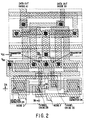
- Fig. 2 is a schematic diagram illustrating a layout of the Fig. 1 circuit.
- Fig. 3A is a cross-sectional view taken along line AA in Fig. 2.
- Fig. 3B is a cross-sectional view taken along line BB in Fig. 3.
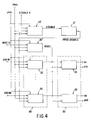
- Fig. 4 is a block diagram illustrating a circuit application in which the nonvolatile latch of the present invention can be used.
- FIG. 1 An embodiment of an electrically alterable nonvolatile latch element in accordance with the present invention, along with an associated high voltage inverter circuit, is illustrated in Fig. 1.
- the basic latch circuit 10 comprises two subcircuits.
- the first subcircuit is a cross-coupled static latch which includes two P-channel field effect transistors 12 and 14 and two N-channel field effect transistors 16 and 18.
- the second subcircuit includes two nonvolatile memory transistors 21 and 22.
- the drains of transistors 12 and 16 are coupled to each other at node A.
- the drains of transistors 14 and 18 are coupled to each other at node B.
- the sources of transistors 12 and 14 are connected to the positive supply potential VCC.
- the sources of transistors 16 and 18 are connected to the ground potential VSS.
- the gates of transistors 12 and 16 are coupled together and are also coupled to node B.
- Transistors 21 and 22 are N-channel floating gate MOSFET devices in which the floating gates are formed in a polysilicon layer and the control gates are selectively defined in the bulk silicon by a buried N+ implant mask.
- the floating gate (node C) of the memory transistor 21 is capacitively coupled to its control gate (node D) via coupling capacitor 24.
- Coupling capacitor 24 is essentially formed by the overlap of the floating polysilicon gate and the buried N+ implant area exposed by the thin oxide mask, as illustrated in Fig. 3A.
- the floating gate (node E) of the memory transistor 22 is capacitively coupled to its control gate (node F) via the coupling capacitor 26.
- the floating gates of the transistors 21 and 22 are capacitively cross-coupled to the control gates of transistors 22 and 21, respectively, via relatively small area tunneling capacitors 28 and 30.
- the tunneling capacitors 30 and 28 are formed by the overlap of the floating gates of transistors 21 and 22 with the buried N+ implant areas which are exposed by the thin oxide mask and are electrically in common with the control gates of transistors 22 and 21, respectively.
- Both the coupling capacitors 24, 26 and the tunneling capacitors 28, 30 have relatively thin oxide (100 Angstroms) dielectrics between the floating gates and the control gates.
- the drain of the memory element 21 is coupled to node B, which was defined in conjunction with the cross-coupled static latch.
- the drain of the memory element 22 is coupled to node A, which was previously defined.
- the sources of both memory elements 21 and 22 are connected to the ground potential VSS.
- stray capacitances inherent in the layout of the latch shown in Fig. 2. These include the floating gate to control gate overlap capacitances in the nonthin-oxide areas and the capacitance due to the source and drain overlap to the floating gate in the memory transistors.
- Figs. 3A and 3B show the cross-sectional views of the memory cell element along the cross-sections AA and BB as indicated on the layout of the latch in Fig. 2.
- region 300 comprises the P-type silicon in which the highly doped N+ source and drain regions are formed for the N-channel CMOS transistors. Also formed in the region 300 are buried-N+ diffusions which are not as highly doped compared to the source/drain N+ regions. The buried-N+ regions are used to form the control gates of the memory transistors and can also be used for conductive underpasses in other parts of the circuitry.
- the control gates of transistors 21 and 22 are shown in the cross-sectional diagrams of Figs. 3A and 3B.
- the floating gates of transistors 21 and 22 are also shown in Figs. 3A and 3B and are comprised of conductive polycrystalline silicon.
- the floating polycrystalline gate of transistor 21 is separated from the crystalline silicon by the coupling oxide 24, the tunneling oxide 28, the gate oxide 31, the oxide over the buried-N+ region 301, and the field oxide 302.
- the oxide over the buried N+, region 301 is substantially thicker than the gate oxides 30 and 32.
- the field oxide, region, 302 is substantially thicker than the oxide in region 301.
- the floating gate of the transistor 21 is also capacitively coupled to its own control gate due to the overlap of the floating polysilicon gate to its control gate formed by the oxide over the buried-N+ region in the silicon substrate, "Cbn+g.”
- Another component of the capacitance, "Cfld,” is due to the overlap of the floating polysilicon gate to the substrate in the field oxide regions 302.
- a high programming voltage "VPPI" (12-17v) must be applied to one of the two programming nodes D or F for about 5-10 ms.
- VPPI high programming voltage
- the other programming node F must be held at the ground potential.
- Rg Ccoup + Cbn+g Ccoup + Cbn+g + Ctun + Cfld + Cgox + Cbn+t
- the initial electric field "E” is of the order of 9-10 Mv/cm, then a sufficient number of electrons tunnel through the tunnel oxide onto the floating gate of transistor 21 storing a net negative charge on node C so as to make an appreciable positive shift in the threshold voltage of this device.
- E VPPI - Rg ⁇ VPPI Ttun
- the initial electric field "E" is of the order of 9-10 Mv/cm, then a sufficient number of electrons tunnel through the tunnel oxide out of the floating gate of transistor 22 storing a net positive charge on node E so as to make an appreciable negative shift in the threshold voltage of this device.
- the field "E” however decreases with time as more and more electrons tunnel through the tunnel oxide and are collected on the floating polycrystalline gate.
- the electric field "E” is so low that very few electrons tunnel through the oxide and further threshold voltage shift is negligible.
- the initial electric field "E′” sets up a Fowler Nordheim conduction which follows the relationship: where: a, a1, B, B1 are physical constants which depend on the effective energy barrier heights at the injection interfaces and the effective mass ratio of electrons in the tunnel dielectric. A is the area of the tunnel dielectric.
- the electric field “E′” also decreases with time as more electrons tunnel through the tunnel oxide out of the floating gate and eventually leaving the floating gate with a net positive charge.
- the electric field “E′” at this point is so low that very few electrons tunnel through the tunnel oxide and further threshold voltage shift is negligible.
- the control gates of both the memory elements are held at the ground potential and the electric fields across the tunnel oxides are minimal and are only due to the charges on the floating gates due to the programming operation.
- the two memory elements in the electrically alterable latch remain programmed to their respective ERASED (enhancement) and WRITTEN (depletion) states.
- ERASED enhanced
- WRITTEN depletion
- node B pulls up to VCC and node A is pulled down to VSS.
- the two cross-coupled inverters are latched to their proper states and no dc power is consumed by the circuit.
- the current sinking capability of the written memory element should be such that it can pull the corresponding cross-coupled latch node low enough to set the latch to its proper programmed state.
- the basic latch circuit 10 described above can be used in conjunction with a high voltage inverter circuit 20, as shown in Fig. 1.
- the purpose of the circuit 20 is to translate the low (VSS) and high (VCC) CMOS levels at its input into high ( ⁇ VPPI 12-17v) and low (VSS) levels respectively.
- circuit 20 works like a high voltage inverter.
- a similar circuit block 20 is also connected to the control gate of memory element 22 shown in Fig. 1. This circuit can be used to reset the DATAOUT (Node B) of the nonvolatile latch to a low (VSS) state, by taking the RESETB signal low during the program cycle.
- Fig. 4 shows one possible setup in which the nonvolatile latch could be used.
- Circuit block 30 includes an "N" bit long register which has the nonvolatile latch circuit 10 described above as the basic building block.
- the circuit block 40 includes "N" high voltage inverter circuits 20 described above, the outputs of each feeding into the input of a corresponding nonvolatile latch 10 in the block 30.
- the top circuit block 20′ has "PROGB” and “PROG-DISABLEB” as the other inputs and its output “DISABLE” feeds into the control gate of one of the memory elements of the additional circuit block 10′.
- the control gate of the other memory element in the circuit block 10 is connected to VSS.
- the output "PROG-DISABLE" of the circuit block 10 serves as a common input to the remaining N+1 high voltage inverters.
- the second high voltage inverter 20 ⁇ outside of the circuit block 40 has its last remaining input connected to a signal called "RESETB" and its output “RESET” is connected to one input of each nonvolatile element in the circuit block 30.
- the last input of each high voltage inverter element in the circuit block 40 is connected to the input of the corresponding nonvolatile latch in the circuit block 30 as shown in Fig. 4.
- the bit pattern A0-A7 should be identical to the desired bit pattern ADD1 - ADDN that was input to the circuit block 40.
Landscapes
- Read Only Memory (AREA)
- Static Random-Access Memory (AREA)
- Non-Volatile Memory (AREA)
- Semiconductor Memories (AREA)
Claims (4)
- Elément de registre à verrouillage non-volatile programmable de façon électrique (10), comprenant :(a) un élément de registre à verrouillage statique comprenant des premier et deuxième éléments inverseurs (12+16; 14+18) reliés de façon croisée dans lesquels la sortie (A) du premier élément inverseur est connectée à l'entrée du deuxième élément inverseur et la sortie (B) du deuxième élément inverseur et connectée à l'entrée du premier élément inverseur;(b) un premier élément de stockage non-volatile (21) qui stocke un premier état de charge, le premier élément de stockage étant connecté pour fournir le premier état de charge à l'entrée du premier élément inverseur dans des conditions présélectionnées;(c) un deuxième élément de stockage non-volatile (22) qui stocke un deuxième état de charge complémentaire au premier état de charge, le deuxième élément de stockage étant connecté pour fournir le deuxième état de charge sur l'entrée du deuxième élément inverseur dans des conditions présélectionnées;(d) des moyens (20) pour programmer l'élément de registre à verrouillage pour stocker de façon sélective soit un premier état logique soit un deuxième état logique dans le premier ou deuxième élément de stockage non-volatile tout en stockant simultanément un état logique opposé dans l'autre élément de stockage volatile, caractérisé en ce quelesdits moyens de programmation (20) comprennent, pour chacun desdits éléments de stockage non-volatile (21, 22) un circuit inverseur comprenant :- des dispositifs FET complémentaires (34, 36) ayant leur drain reliés ensemble et à une électrode de commande (D) de l'élément de stockage non-volatile respectif, leurs sources étant respectivement connectées à un potentiel prédéterminé (VSS) et à une tension de programmation (VPPI), et leurs grilles étant reliées ensemble à un potentiel d'activation (G);- un autre dispositif FET (38) dont la source et le drain sont reliés respectivement audit potentiel d'activation (G) et à ladite tension de programmation (VPPI) et dont la grille est connectée à ladite électrode de commande (D).
- Elément de registre à verrouillage non-volatile programmable de façon électrique selon la revendication 1 dans lequel ledit élément de registre à verrouillage statique comprend des premier et deuxième FET à canal P (12, 14) et des premier et deuxième FET à canal N (16, 18) les drains du premier FET à canal P et du premier FET à canal N et du deuxième FET à canal P et du deuxième FET à canal N étant respectivement reliés en commun, les sources du premier et du second FET à canal P étant connectées en commun à un premier potentiel (VCC), les sources du premier et du deuxième FET à canal N étant connectées en commun à un deuxième potentiel (VSS) plus négatif que le premier potentiel, les grilles du premier FET à canal P et du premier FET à canal N étant connectées en commun aux drain du premier élément de stockage non-volatile (21) et à une première sortie (D), les grilles du deuxième FET à canal P et du deuxième FET à canal N étant connectées en commun au drain du deuxième élément de stockage non-volatile (22) et à une deuxième sortie (A), les source du premier et du second élément de stockage étant connectées en commun au deuxième potentiel.
- Elément de registre à verrouillage non-volatile programmable de façon électrique selon la revendication 2 comprenant un couplage capacitif entre la grille flottante et la grille de commande du premier et du deuxième élément de stockage via des premier et deuxième condensateurs de couplage (24, 26) respectivement, chacun desdits condensateurs de couplage étant formé par le recouvrement de sa grille flottante associée et d'une zone implantée N+ enterrée séparée de ladite grille flottante associée par une couche diélectrique.
- Elément de registre à verrouillage non-volatile programmable de façon électrique selon la revendication 3 dans lequel les grilles flottantes du premier et du deuxième éléments de stockage sont couplées de façon croisée et de façon capacitive à la grille de commande du premier et du deuxième éléments de stockage respectivement, via des premier et un deuxième condensateurs à effet tunnel (28, 30) respectivement, chacun desdits condensateurs à effet tunnel étant formé par un recouvrement de sa grille flottante associée et d'une zone implantée N+ enterrée séparée de ladite grille flottante associée par une couche diélectrique.
Applications Claiming Priority (2)
| Application Number | Priority Date | Filing Date | Title |
|---|---|---|---|
| US149568 | 1988-01-28 | ||
| US07/149,568 US4858185A (en) | 1988-01-28 | 1988-01-28 | Zero power, electrically alterable, nonvolatile latch |
Publications (3)
| Publication Number | Publication Date |
|---|---|
| EP0326883A2 EP0326883A2 (fr) | 1989-08-09 |
| EP0326883A3 EP0326883A3 (fr) | 1991-07-10 |
| EP0326883B1 true EP0326883B1 (fr) | 1994-12-28 |
Family
ID=22530876
Family Applications (1)
| Application Number | Title | Priority Date | Filing Date |
|---|---|---|---|
| EP89101040A Expired - Lifetime EP0326883B1 (fr) | 1988-01-28 | 1989-01-21 | Bascule non volatile, électriquement modifiable à consommation nulle |
Country Status (5)
| Country | Link |
|---|---|
| US (1) | US4858185A (fr) |
| EP (1) | EP0326883B1 (fr) |
| JP (1) | JP2831015B2 (fr) |
| CA (1) | CA1303689C (fr) |
| DE (1) | DE68920161T2 (fr) |
Cited By (6)
| Publication number | Priority date | Publication date | Assignee | Title |
|---|---|---|---|---|
| US7791950B2 (en) | 2005-03-17 | 2010-09-07 | Virage Logic Corporation | Inverter non-volatile memory cell and array system |
| US7796450B1 (en) | 2007-04-24 | 2010-09-14 | Virage Logic Corporation | Radio frequency (RFID) tag including configurable single bit/dual bits memory |
| US7808823B2 (en) | 2005-03-31 | 2010-10-05 | Virage Logic Corporation | RFID tag with redundant non-volatile memory cell |
| US8077511B2 (en) | 2004-04-21 | 2011-12-13 | Synopsys, Inc. | Hybrid non-volatile memory |
| US8111558B2 (en) | 2004-05-05 | 2012-02-07 | Synopsys, Inc. | pFET nonvolatile memory |
| DE102015220839B4 (de) | 2015-10-26 | 2023-01-12 | Brose Fahrzeugteile Se & Co. Kommanditgesellschaft, Bamberg | Verfahren und Vorrichtung zur Ermittlung der Stellposition eines verstellbaren Kraftfahrzeugteils |
Families Citing this family (38)
| Publication number | Priority date | Publication date | Assignee | Title |
|---|---|---|---|---|
| JP2832998B2 (ja) * | 1989-04-27 | 1998-12-09 | 日本電気株式会社 | 不揮発性mos半導体記憶装置 |
| US5272368A (en) * | 1991-05-10 | 1993-12-21 | Altera Corporation | Complementary low power non-volatile reconfigurable EEcell |
| US5644533A (en) * | 1992-11-02 | 1997-07-01 | Nvx Corporation | Flash memory system, and methods of constructing and utilizing same |
| US5548228A (en) * | 1994-09-28 | 1996-08-20 | Altera Corporation | Reconfigurable programmable logic device having static and non-volatile memory |
| US5625211A (en) * | 1995-01-12 | 1997-04-29 | Actel Corporation | Two-transistor electrically-alterable switch employing hot electron injection and fowler nordheim tunneling |
| JP2961126B2 (ja) * | 1995-02-13 | 1999-10-12 | セントラル硝子株式会社 | 三次元光メモリーガラス素子からなる記録媒体及びその記録方法 |
| US5596524A (en) * | 1995-04-21 | 1997-01-21 | Advanced Micro Devices, Inc. | CMOS memory cell with gate oxide of both NMOS and PMOS transistors as tunneling window for program and erase |
| US5754471A (en) * | 1995-06-06 | 1998-05-19 | Advanced Micro Devices, Inc. | Low power CMOS array for a PLD with program and erase using controlled avalanche injection |
| US5801985A (en) | 1995-07-28 | 1998-09-01 | Micron Technology, Inc. | Memory system having programmable control parameters |
| US5682345A (en) * | 1995-07-28 | 1997-10-28 | Micron Quantum Devices, Inc. | Non-volatile data storage unit method of controlling same |
| US5627784A (en) * | 1995-07-28 | 1997-05-06 | Micron Quantum Devices, Inc. | Memory system having non-volatile data storage structure for memory control parameters and method |
| US5657444A (en) * | 1995-08-03 | 1997-08-12 | National Semiconductor Corporation | Microprocessor with secure programmable read only memory circuit |
| US5587945A (en) * | 1995-11-06 | 1996-12-24 | Advanced Micro Devices, Inc. | CMOS EEPROM cell with tunneling window in the read path |
| US5793775A (en) * | 1996-01-26 | 1998-08-11 | Micron Quantum Devices, Inc. | Low voltage test mode operation enable scheme with hardware safeguard |
| US5694055A (en) * | 1996-02-27 | 1997-12-02 | Philips Electronic North America Corp. | Zero static power programmable logic cell |
| US5646901A (en) * | 1996-03-26 | 1997-07-08 | Advanced Micro Devices, Inc. | CMOS memory cell with tunneling during program and erase through the NMOS and PMOS transistors and a pass gate separating the NMOS and PMOS transistors |
| US6122191A (en) * | 1996-05-01 | 2000-09-19 | Cypress Semiconductor Corporation | Semiconductor non-volatile device including embedded non-volatile elements |
| SE509159C2 (sv) * | 1997-01-27 | 1998-12-07 | Ericsson Telefon Ab L M | Hållkrets jämte förfarande för styrning av en hållkrets |
| US5781471A (en) * | 1997-08-15 | 1998-07-14 | Programmable Microelectronics Corporation | PMOS non-volatile latch for storage of redundancy addresses |
| US6141247A (en) * | 1997-10-24 | 2000-10-31 | Micron Technology, Inc. | Non-volatile data storage unit and method of controlling same |
| US5943268A (en) * | 1997-12-31 | 1999-08-24 | Programmable Microelectronics Corporation | Non-volatile latch having PMOS floating gate memory cells |
| US5986962A (en) * | 1998-07-23 | 1999-11-16 | International Business Machines Corporation | Internal shadow latch |
| JP2001358313A (ja) * | 2000-06-14 | 2001-12-26 | Hitachi Ltd | 半導体装置 |
| ITRM20010556A1 (it) * | 2001-09-12 | 2003-03-12 | Micron Technology Inc | Decodificatore per decodificare i comandi di commutazione a modo di test di circuiti integrati. |
| US7145370B2 (en) | 2003-09-05 | 2006-12-05 | Impinj, Inc. | High-voltage switches in single-well CMOS processes |
| US7177182B2 (en) * | 2004-03-30 | 2007-02-13 | Impinj, Inc. | Rewriteable electronic fuses |
| US7388420B2 (en) * | 2004-03-30 | 2008-06-17 | Impinj, Inc. | Rewriteable electronic fuses |
| US7242614B2 (en) | 2004-03-30 | 2007-07-10 | Impinj, Inc. | Rewriteable electronic fuses |
| US7859925B1 (en) | 2006-03-31 | 2010-12-28 | Cypress Semiconductor Corporation | Anti-fuse latch self-test circuit and method |
| US8122307B1 (en) | 2006-08-15 | 2012-02-21 | Synopsys, Inc. | One time programmable memory test structures and methods |
| US7859906B1 (en) | 2007-03-30 | 2010-12-28 | Cypress Semiconductor Corporation | Circuit and method to increase read margin in non-volatile memories using a differential sensing circuit |
| US7968926B2 (en) * | 2007-12-19 | 2011-06-28 | Taiwan Semiconductor Manufacturing Company, Ltd. | Logic non-volatile memory cell with improved data retention ability |
| US8064255B2 (en) * | 2007-12-31 | 2011-11-22 | Cypress Semiconductor Corporation | Architecture of a nvDRAM array and its sense regime |
| US8036032B2 (en) * | 2007-12-31 | 2011-10-11 | Cypress Semiconductor Corporation | 5T high density NVDRAM cell |
| US8059458B2 (en) * | 2007-12-31 | 2011-11-15 | Cypress Semiconductor Corporation | 3T high density nvDRAM cell |
| US7894261B1 (en) | 2008-05-22 | 2011-02-22 | Synopsys, Inc. | PFET nonvolatile memory |
| TWI469325B (zh) | 2012-07-31 | 2015-01-11 | 財團法人工業技術研究院 | 邏輯閘 |
| TWI493548B (zh) | 2013-01-31 | 2015-07-21 | Ind Tech Res Inst | 可組態邏輯區塊及其操作方法 |
Family Cites Families (13)
| Publication number | Priority date | Publication date | Assignee | Title |
|---|---|---|---|---|
| US4095281A (en) * | 1976-03-04 | 1978-06-13 | Rca Corporation | Random access-erasable read only memory cell |
| US4132904A (en) * | 1977-07-28 | 1979-01-02 | Hughes Aircraft Company | Volatile/non-volatile logic latch circuit |
| US4486769A (en) * | 1979-01-24 | 1984-12-04 | Xicor, Inc. | Dense nonvolatile electrically-alterable memory device with substrate coupling electrode |
| US4409723A (en) * | 1980-04-07 | 1983-10-18 | Eliyahou Harari | Method of forming non-volatile EPROM and EEPROM with increased efficiency |
| US4328565A (en) * | 1980-04-07 | 1982-05-04 | Eliyahou Harari | Non-volatile eprom with increased efficiency |
| FR2517142A1 (fr) * | 1981-11-20 | 1983-05-27 | Efcis | Bascule bistable a stockage non volatil et a repositionnement statique |
| FR2517143A1 (fr) * | 1981-11-20 | 1983-05-27 | Efcis | Bascule bistable a stockage non volatil et a repositionnement dynamique |
| US4408303A (en) * | 1981-12-28 | 1983-10-04 | Mostek Corporation | Directly-coupled and capacitively coupled nonvolatile static RAM cell |
| US4571704A (en) * | 1984-02-17 | 1986-02-18 | Hughes Aircraft Company | Nonvolatile latch |
| US4628487A (en) * | 1984-08-14 | 1986-12-09 | Texas Instruments Incorporated | Dual slope, feedback controlled, EEPROM programming |
| US4599706A (en) * | 1985-05-14 | 1986-07-08 | Xicor, Inc. | Nonvolatile electrically alterable memory |
| US4695979A (en) * | 1985-09-09 | 1987-09-22 | Texas Instruments Incorporated | Modified four transistor EEPROM cell |
| JPS6414798A (en) * | 1987-07-09 | 1989-01-18 | Fujitsu Ltd | Non-volatile memory device |
-
1988
- 1988-01-28 US US07/149,568 patent/US4858185A/en not_active Expired - Lifetime
-
1989
- 1989-01-21 EP EP89101040A patent/EP0326883B1/fr not_active Expired - Lifetime
- 1989-01-21 DE DE68920161T patent/DE68920161T2/de not_active Expired - Lifetime
- 1989-01-27 CA CA000589321A patent/CA1303689C/fr not_active Expired - Fee Related
- 1989-01-30 JP JP1017849A patent/JP2831015B2/ja not_active Expired - Lifetime
Cited By (6)
| Publication number | Priority date | Publication date | Assignee | Title |
|---|---|---|---|---|
| US8077511B2 (en) | 2004-04-21 | 2011-12-13 | Synopsys, Inc. | Hybrid non-volatile memory |
| US8111558B2 (en) | 2004-05-05 | 2012-02-07 | Synopsys, Inc. | pFET nonvolatile memory |
| US7791950B2 (en) | 2005-03-17 | 2010-09-07 | Virage Logic Corporation | Inverter non-volatile memory cell and array system |
| US7808823B2 (en) | 2005-03-31 | 2010-10-05 | Virage Logic Corporation | RFID tag with redundant non-volatile memory cell |
| US7796450B1 (en) | 2007-04-24 | 2010-09-14 | Virage Logic Corporation | Radio frequency (RFID) tag including configurable single bit/dual bits memory |
| DE102015220839B4 (de) | 2015-10-26 | 2023-01-12 | Brose Fahrzeugteile Se & Co. Kommanditgesellschaft, Bamberg | Verfahren und Vorrichtung zur Ermittlung der Stellposition eines verstellbaren Kraftfahrzeugteils |
Also Published As
| Publication number | Publication date |
|---|---|
| US4858185A (en) | 1989-08-15 |
| EP0326883A2 (fr) | 1989-08-09 |
| JPH027290A (ja) | 1990-01-11 |
| CA1303689C (fr) | 1992-06-16 |
| EP0326883A3 (fr) | 1991-07-10 |
| DE68920161T2 (de) | 1995-07-27 |
| JP2831015B2 (ja) | 1998-12-02 |
| DE68920161D1 (de) | 1995-02-09 |
Similar Documents
| Publication | Publication Date | Title |
|---|---|---|
| EP0326883B1 (fr) | Bascule non volatile, électriquement modifiable à consommation nulle | |
| US7430137B2 (en) | Non-volatile memory cells in a field programmable gate array | |
| JP2685770B2 (ja) | 不揮発性半導体記憶装置 | |
| US6700821B2 (en) | Programmable mosfet technology and programmable address decode and correction | |
| KR0145475B1 (ko) | 낸드구조를 가지는 불휘발성 반도체 메모리의 프로그램장치 및 방법 | |
| US4571704A (en) | Nonvolatile latch | |
| EP0467928B1 (fr) | Cellules de memoire vive non volatile amelioree utilisant deux elements differentiels de memoire non volatile pouvant etre desaccouples | |
| US5523971A (en) | Non-volatile memory cell for programmable logic device | |
| EP0463580B1 (fr) | Dispositif de mémoire non-volatile à semi-conducteurs | |
| US6240020B1 (en) | Method of bitline shielding in conjunction with a precharging scheme for nand-based flash memory devices | |
| US5748527A (en) | Nonvolatile memory having transistor redundancy | |
| US5912937A (en) | CMOS flip-flop having non-volatile storage | |
| US6100746A (en) | Electrically programmable fuse | |
| EP0459246A2 (fr) | Registre EPROM | |
| US7092293B1 (en) | Non-volatile memory cell integrated with a latch | |
| EP0326053B1 (fr) | Méthode de protection de données pour une mémoire programmable | |
| GB2061045A (en) | Nonvolatile static random access memory system | |
| EP0377841B1 (fr) | Circuit intégré à semi-conducteurs capable d'éviter une occurrence d'opération erronée due au bruit | |
| KR20010013737A (ko) | 비휘발성 반도체 저장 장치용 구동 회로 | |
| KR100616720B1 (ko) | 고정 메모리 셀 장치를 프로그래밍하는 방법 | |
| JP2579346B2 (ja) | 半導体不揮発性記憶素子 | |
| Wright et al. | An SRAM cell with nonvolatile memory for programmable logic applications | |
| EP0295036B1 (fr) | Dispositif de mémoire à semi-conducteurs | |
| Op't Eynde et al. | An EEPROM in a standard CMOS technology | |
| KR0172336B1 (ko) | 불 휘발성 반도체 메모리의 프로그램 검증 및 금지 방법과 그 회로 |
Legal Events
| Date | Code | Title | Description |
|---|---|---|---|
| PUAI | Public reference made under article 153(3) epc to a published international application that has entered the european phase |
Free format text: ORIGINAL CODE: 0009012 |
|
| AK | Designated contracting states |
Kind code of ref document: A2 Designated state(s): DE FR GB IT NL |
|
| PUAL | Search report despatched |
Free format text: ORIGINAL CODE: 0009013 |
|
| AK | Designated contracting states |
Kind code of ref document: A3 Designated state(s): DE FR GB IT NL |
|
| 17P | Request for examination filed |
Effective date: 19911214 |
|
| 17Q | First examination report despatched |
Effective date: 19921201 |
|
| GRAA | (expected) grant |
Free format text: ORIGINAL CODE: 0009210 |
|
| AK | Designated contracting states |
Kind code of ref document: B1 Designated state(s): DE FR GB IT NL |
|
| PG25 | Lapsed in a contracting state [announced via postgrant information from national office to epo] |
Ref country code: IT Free format text: LAPSE BECAUSE OF FAILURE TO SUBMIT A TRANSLATION OF THE DESCRIPTION OR TO PAY THE FEE WITHIN THE PRE;WARNING: LAPSES OF ITALIAN PATENTS WITH EFFECTIVE DATE BEFORE 2007 MAY HAVE OCCURRED AT ANY TIME BEFORE 2007. THE CORRECT EFFECTIVE DATE MAY BE DIFFERENT FROM THE ONE RECORDED.SCRIBED TIME-LIMIT Effective date: 19941228 Ref country code: FR Effective date: 19941228 Ref country code: NL Effective date: 19941228 |
|
| REF | Corresponds to: |
Ref document number: 68920161 Country of ref document: DE Date of ref document: 19950209 |
|
| PG25 | Lapsed in a contracting state [announced via postgrant information from national office to epo] |
Ref country code: GB Effective date: 19950328 |
|
| EN | Fr: translation not filed | ||
| NLV1 | Nl: lapsed or annulled due to failure to fulfill the requirements of art. 29p and 29m of the patents act | ||
| PLBE | No opposition filed within time limit |
Free format text: ORIGINAL CODE: 0009261 |
|
| STAA | Information on the status of an ep patent application or granted ep patent |
Free format text: STATUS: NO OPPOSITION FILED WITHIN TIME LIMIT |
|
| GBPC | Gb: european patent ceased through non-payment of renewal fee |
Effective date: 19950328 |
|
| 26N | No opposition filed | ||
| PGFP | Annual fee paid to national office [announced via postgrant information from national office to epo] |
Ref country code: DE Payment date: 20080229 Year of fee payment: 20 |