EP0326996A2 - Integrierte Halbleiterschaltung mit einer Pegelumsetzungsschaltung - Google Patents
Integrierte Halbleiterschaltung mit einer Pegelumsetzungsschaltung Download PDFInfo
- Publication number
- EP0326996A2 EP0326996A2 EP89101570A EP89101570A EP0326996A2 EP 0326996 A2 EP0326996 A2 EP 0326996A2 EP 89101570 A EP89101570 A EP 89101570A EP 89101570 A EP89101570 A EP 89101570A EP 0326996 A2 EP0326996 A2 EP 0326996A2
- Authority
- EP
- European Patent Office
- Prior art keywords
- line
- circuit
- voltage line
- ground line
- voltage
- Prior art date
- Legal status (The legal status is an assumption and is not a legal conclusion. Google has not performed a legal analysis and makes no representation as to the accuracy of the status listed.)
- Granted
Links
Images

Classifications
-
- H—ELECTRICITY
- H03—ELECTRONIC CIRCUITRY
- H03K—PULSE TECHNIQUE
- H03K19/00—Logic circuits, i.e. having at least two inputs acting on one output; Inverting circuits
- H03K19/0175—Coupling arrangements; Interface arrangements
- H03K19/0185—Coupling arrangements; Interface arrangements using field effect transistors only
- H03K19/018507—Interface arrangements
Definitions
- the present invention relates to a semiconductor integrated circuit, and more specifically to a signal level conversion circuit for use in a socalled BiMOS semiconductor logic integrated circuit composed of bipolar transistors and MOS transistors which are formed in a mixed manner on the same single chip.
- the BiCMOS semiconductor logic integrated circuits have been composed of CMOS (complementary metal-oxide-semiconductor) transistors and bipolar transistors formed on the same single chip so that the circuits can have both advantages of the CMOS transistors such as a low power dissipation and a high integration density and advantages of the bipolar transistors such as a high operation speed and a high driving power.
- CMOS complementary metal-oxide-semiconductor
- bipolar transistors such as a high operation speed and a high driving power.
- the BiCMOS logic circuits have already achieved a gate delay time partially overlapping with that obtained in conventional ECL emitter coupled logic) logic circuits. Therefore, it has been expected that the ECL logic circuits will be replaced by the BiCMOS circuits in applications or areas where a relatively large gate delay time is permitted.
- the BiCMOS logic circuits are required to be driven at the same supply voltage level as that of the existing ECL logic circuits.
- the BiCMOS logic circuits are required to be capable of operating at a so-called ECL input/output level by introducing a nominal supply voltage of -4.5V into the chip.
- the BiCMOS logic circuits are preferred to be driven at a so-called TTL input/output level by connecting a nominal supply voltage of +5.0V to the chip.
- the ECL circuits and the TTL circuits are combined on the same signal chip, the chip is connected to both a supply voltage of -4.5V and another supply voltage of +5.0V.
- the conventional signal level conversion circuit has been of a differential circuit type, which is relatively large in power consumption and also needs a substantial number of circuit elements.
- the conventional signal level conversion circuit of the differential circuit type requires at least a pair of active circuit elements such as a pair of bipolar transistors, and needs a constant current source.
- Another object of the present invention is to provide a signal level conversion circuit for use in BiCMOS circuits, which conversion circuit is very simple in construction and can operate at a low power consumption and is composed of a relatively small number of circuit elements.
- Still another object of the present invention is to provide a signal level conversion circuit for use in BiCMOS circuits, which conversion circuit is composed of a single transistor without a constant current source.
- a semiconductor integrated circuit comprising a positive voltage line, a negative voltage line, a ground line, a first circuit connected between the ground line and one of the positive voltage line and the negative voltage line so as to be driven by a voltage difference between the ground line and the one of the positive voltage line and the negative voltage line, a second circuit connected between the ground line and the other of the positive voltage line and the negative voltage line so as to be driven by a voltage difference between the ground line and the other of the positive voltage line and the negative voltage line, and a signal level conversion circuit including a MOS transistor having a gate connected to an output of the first circuit and a drain connected through a resistor to the ground line, a source of the transistor being connected to the other of the positive voltage line and the negative voltage line, the drain of the transistor being connected to an input of the second circuit, the transistor having its threshold voltage whose absolute value is larger than an absolute value of a voltage difference between the ground line and the other of the positive voltage line and the negative voltage line and the negative
- the MOS transistor has its threshold voltage whose absolute value is substantially equal to a sum of the absolute value of the voltage difference between the ground line and the other of the positive voltage line and the negative voltage line, and an absolute value of a threshold voltage of the first circuit.
- the first circuit is composed of an ECL circuit connected between the ground line and the negative voltage line so as to be driven by a voltage difference between the ground line and the negative voltage line
- the second circuit is composed of a TTL circuit connected between the ground line and the positive voltage line so as to be driven by a voltage difference between the ground line and the positive voltage line
- the MOS transistor is of a p-channel type whose source is connected to the positive voltage line, the p-channel MOS transistor having its threshold voltage whose absolute value is larger than an absolute value of a voltage difference between the ground line and the positive voltage line, so that an output signal of the ECL circuit whose potential varies between the ground line and the negative voltage line, is converted into a signal whose potential varies between the ground line and the positive voltage line.
- the p-channel MOS transistor has its threshold voltage whose absolute value is substantially equal to a sum of the absolute value of the voltage difference between the ground line and the positive voltage line, and an absolute value of a threshold voltage of the ECL circuit.
- the first circuit is composed of a TTL circuit connected between the ground line and the positive voltage line so as to be driven by a voltage difference between the ground line and the positive voltage line
- the second circuit is composed of an ECL circuit connected between the ground line and the negative voltage line so as to be driven by a voltage difference between the ground line and the negative voltage line
- the MOS transistor is of a n-channel type whose source is connected to the negative voltage line, the n-channel MOS transistor having its threshold voltage whose absolute value is larger than an absolute value of a voltage difference between the ground line and the negative voltage line, so that an output signal of the TTL circuit whose potential varies between the ground line and the positive voltage line, is converted into a signal whose potential varies between the ground line and the negative voltage line.
- the n-channel MOS transistor has its threshold voltage whose absolute value is substantially equal to a sum of the absolute value of the voltage difference between the ground line and the negative voltage line, and an absolute value of a threshold voltage of the TTL circuit.
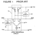
- FIG. 1 there is shown a circuit block diagram of a conventional signal level conversion circuit for use in BiCMOS circuits.
- the shown BiCMOS circuit includes a ECL circuit 10 connected between a negative voltage supply V EE and ground GND, and an TTL circuit 12 connected between a positive voltage supply V CC and the ground GND.
- a signal level conversion circuit 14 coupled between the ECL circuit 10 and the TTL circuit 12 is composed of a differential circuit, which includes a first bipolar transistor 16 connected at its base to an output of the ECL circuit 10 and a second bipolar transistor 18 connected at its base to receive a reference voltage V R . Respective emitters of these transistors 16 and 18 are commonly connected to each other and also connected through a constant current source 20 to the negative voltage supply V EE .
- collectors of the transistors 16 and 18 are connected through resistors 22 and 24 to the positive voltage supply V CC , respectively.
- a connection node between the collector of each transistor and the corresponding resistor is connected to a corresponding one of a pair of inputs of the TTL circuit 12.
- the output signal of the ECL circuit 10 varying between the ground level GND and the negative voltage V EE is converted to a signal varying between the positive voltage V CC and the ground level GND.
- the signal level conversion circuit 14 In the signal level conversion circuit 14, however, an electric current of a few milliamperes continues to flow in the differential circuit connected between the positive voltage supply V CC and the negative voltage supply V EE . In other words, if the positive voltage supply V CC is +5.0V and the negative voltage supply V EE is -4.5V, the electric current of a few milliamperes is ceaselessly flowed across a potential difference of about 10V. This is a substantial electric power consumption in the conventional signal level conversion circuit shown in Figure 1.
- the differential circuit has needed a pair of transistors 16 and 18, and one load resistor (22 or 24) has been required for each of the pair of transistors.
- the constant current source 20 has been associated to the differential circuit. Therefore, the signal level conversion circuit 14 has needed a substantial number of circuit elements, which would accordingly occupy a substantial chip area.
- FIG. 2 there is shown a circuit block diagram of one embodiment of the signal level conversion circuit in accordance with the present invention for use in BiCMOS circuits.
- the shown BiCMOS circuit includes an ECL circuit 30 connected between a negative voltage supply V EE and ground GND, and a TTL circuit 32 connected between a positive voltage supply V CC and the ground GND.
- a p-channel MOS transistor 34 is connected at its gate to an output of the ECL circuit 30 and at its source to the positive voltage supply V CC .
- a drain of the transistor 34 is connected through a resistor 36 to the ground GND and a connection node "A" between the drain of the transistor 34 and the resistor 36 is connected to an input of the TTL circuit 32.
- the transistor 34 and the resistor 36 constitutes a signal level conversion circuit.
- the p-channel MOS transistor 34 is designed to have a threshold voltage V TP whose absolute value
- V TP -6.3V.
- V TP -7.6V.
- the ECL circuit 30 outputs a signal of a low level "L"
- the p-channel MOS transistor 34 is brought into an ON condition. Therefore, the node “A” is elevated to a level near to the positive voltage V CC , and accordingly, a signal of a high level “H” is inputted to the TTL circuit 32.
- the ECL circuit 30 outputs a signal of a high level "H"
- the p-channel MOS transistor 34 is brought into an OFF condition.
- the node "A” is pulled down to a level near to the voltage of the ground GND, and accordingly, a signal of a low level “L” is inputted to the TTL circuit 32.
- FIG. 3 there is shown a circuit block diagram of another embodiment of the signal level conversion circuit in accordance with the present invention for use in BiCMOS circuits.
- the shown BiCMOS circuit includes a TTL circuit 40 connected between a positive voltage supply V CC and ground GND and an ECL circuit 42 connected between a negative voltage supply V EE and the ground GND.
- a n-channel MOS transistor 44 is connected at its gate to an output of the TTL circuit 40 and at its source to the negative voltage supply V EE .
- a drain of the transistor 44 is connected through a resistor 46 to the ground GND and a connection node "B" between the drain of the transistor 44 and the resistor 46 is connected to an input of the ECL circuit 42.
- the transistor 44 and the resistor 46 constitutes a signal level conversion circuit.
- the n-channel MOS transistor 44 is designed to have a threshold voltage V TN whose absolute value
- V TN 6.6V
- V TP 7.7V
- the TTL circuit 40 outputs a signal of a high level "H"
- the n-channel MOS transistor 44 is brought into an ON condition. Accordingly, the node “B” is pulled down to a level near to the negative voltage V EE , and accordingly, a signal of a low level “L” is inputted to the ECL circuit 42.
- the TTL circuit 40 outputs a signal of a low level "L"
- the n-channel MOS transistor 44 is brought into an OFF condition. Therefore, the node “B” is elevated to a level near to the voltage of the ground GND, and accordingly, a signal of a high level “H” is inputted to the ECL circuit 42.
- the signal level conversion circuit in accordance with the present invention can effectively convert a signal level without substantial power consumption, and therefore, can be used or formed in a BiCMOS semiconductor integrated circuit of a low power consumption. Furthermore, the signal level conversion circuit in accordance with the present invention is very simple in construction and is composed of a very small number of circuit elements, and accordingly, can be assembled or formed in a small chip area. This feature is very advantageous to increase of the integration density of the integrated circuit.
Landscapes
- Engineering & Computer Science (AREA)
- Computer Hardware Design (AREA)
- Physics & Mathematics (AREA)
- Computing Systems (AREA)
- General Engineering & Computer Science (AREA)
- Mathematical Physics (AREA)
- Logic Circuits (AREA)
Applications Claiming Priority (2)
| Application Number | Priority Date | Filing Date | Title |
|---|---|---|---|
| JP63019751A JPH01195719A (ja) | 1988-01-30 | 1988-01-30 | 半導体集積回路 |
| JP19751/88 | 1988-01-30 |
Publications (3)
| Publication Number | Publication Date |
|---|---|
| EP0326996A2 true EP0326996A2 (de) | 1989-08-09 |
| EP0326996A3 EP0326996A3 (en) | 1990-02-14 |
| EP0326996B1 EP0326996B1 (de) | 1993-11-18 |
Family
ID=12008042
Family Applications (1)
| Application Number | Title | Priority Date | Filing Date |
|---|---|---|---|
| EP89101570A Expired - Lifetime EP0326996B1 (de) | 1988-01-30 | 1989-01-30 | Integrierte Halbleiterschaltung mit einer Pegelumsetzungsschaltung |
Country Status (4)
| Country | Link |
|---|---|
| US (1) | US4977339A (de) |
| EP (1) | EP0326996B1 (de) |
| JP (1) | JPH01195719A (de) |
| DE (1) | DE68910705T2 (de) |
Cited By (1)
| Publication number | Priority date | Publication date | Assignee | Title |
|---|---|---|---|---|
| EP0416323A3 (en) * | 1989-09-04 | 1991-04-24 | Siemens Aktiengesellschaft | Signal level converter |
Families Citing this family (7)
| Publication number | Priority date | Publication date | Assignee | Title |
|---|---|---|---|---|
| US5225721A (en) * | 1991-12-18 | 1993-07-06 | Unisys Corporation | Signal translator for interconnecting CMOS and BiCMOS logic gates |
| US5594368A (en) * | 1995-04-19 | 1997-01-14 | Kabushiki Kaisha Toshiba | Low power combinational logic circuit |
| US5666070A (en) * | 1995-05-10 | 1997-09-09 | Micron Technology, Inc. | Low power, high speed level shifter |
| US5528173A (en) | 1995-05-10 | 1996-06-18 | Micron Technology, Inc. | Low power, high speed level shifter |
| US6212402B1 (en) * | 1996-11-04 | 2001-04-03 | Telefonaktiebolaget Lm Ericsson | System connector |
| JP4148162B2 (ja) * | 2004-03-05 | 2008-09-10 | 株式会社デンソー | 回路システム |
| US20080042722A1 (en) * | 2006-08-15 | 2008-02-21 | Silicon Laboratories, Inc. | High speed level shifter circuit and circuit using same |
Family Cites Families (11)
| Publication number | Priority date | Publication date | Assignee | Title |
|---|---|---|---|---|
| DE2524001A1 (de) * | 1975-05-30 | 1976-12-02 | Licentia Gmbh | Integrierte schaltungsanordnung mit mos-transistoren |
| JPS585029A (ja) * | 1981-06-30 | 1983-01-12 | Fujitsu Ltd | レベル変換回路 |
| US4437171A (en) * | 1982-01-07 | 1984-03-13 | Intel Corporation | ECL Compatible CMOS memory |
| JPS58194430A (ja) * | 1982-05-07 | 1983-11-12 | Nec Corp | インタ−フエ−ス回路 |
| US4453095A (en) * | 1982-07-16 | 1984-06-05 | Motorola Inc. | ECL MOS Buffer circuits |
| JPS5943631A (ja) * | 1982-09-06 | 1984-03-10 | Hitachi Ltd | レベル変換入力回路 |
| US4656372A (en) * | 1985-11-25 | 1987-04-07 | Ncr Corporation | CMOS to ECL interface circuit |
| US4719372A (en) * | 1986-02-03 | 1988-01-12 | International Business Machines Corporation | Multiplying interface circuit for level shifting between FET and TTL levels |
| JPS62230223A (ja) * | 1986-03-31 | 1987-10-08 | Toshiba Corp | 出力回路 |
| US4704549A (en) * | 1986-10-24 | 1987-11-03 | Ncr Corporation | CMOS to ECL converter-buffer |
| US4767951A (en) * | 1987-06-30 | 1988-08-30 | Hewlett-Packard Company | ECL to NMOS converter |
-
1988
- 1988-01-30 JP JP63019751A patent/JPH01195719A/ja active Pending
-
1989
- 1989-01-30 US US07/303,845 patent/US4977339A/en not_active Expired - Fee Related
- 1989-01-30 DE DE89101570T patent/DE68910705T2/de not_active Expired - Fee Related
- 1989-01-30 EP EP89101570A patent/EP0326996B1/de not_active Expired - Lifetime
Cited By (2)
| Publication number | Priority date | Publication date | Assignee | Title |
|---|---|---|---|---|
| EP0416323A3 (en) * | 1989-09-04 | 1991-04-24 | Siemens Aktiengesellschaft | Signal level converter |
| US5122689A (en) * | 1989-09-04 | 1992-06-16 | Siemens Aktiengesellschaft | Cmos to ecl/cml level converter |
Also Published As
| Publication number | Publication date |
|---|---|
| JPH01195719A (ja) | 1989-08-07 |
| DE68910705T2 (de) | 1994-04-21 |
| US4977339A (en) | 1990-12-11 |
| DE68910705D1 (de) | 1993-12-23 |
| EP0326996B1 (de) | 1993-11-18 |
| EP0326996A3 (en) | 1990-02-14 |
Similar Documents
| Publication | Publication Date | Title |
|---|---|---|
| US4920284A (en) | CMOS level converter circuit with reduced power consumption | |
| EP0880230A2 (de) | Spannungspegelverschieber | |
| US4961011A (en) | BiMOS current mirror | |
| KR910006696B1 (ko) | 출력 인터페이스회로 | |
| JPH0436606B2 (de) | ||
| EP0247172B1 (de) | Cmos- zu ecl-schnittstellenschaltung | |
| US5371419A (en) | CMOS well switching circuit | |
| US4538076A (en) | Level converter circuit | |
| US5015888A (en) | Circuit and method of generating logic output signals from an ECL gate to drive a non-ECL gate | |
| EP0326996B1 (de) | Integrierte Halbleiterschaltung mit einer Pegelumsetzungsschaltung | |
| US4798981A (en) | Input circuit | |
| EP0555075A2 (de) | Regelumsetzer mit niedrigem Verbrauch | |
| EP0439158B1 (de) | Schneller Pegelumsetzer | |
| EP0375123A2 (de) | ECL-CMOS-Umsetzer mit einer einzigen Speisespannung | |
| US5162677A (en) | ECL to CMOS level conversion circuit | |
| JPH05315937A (ja) | Cmos/eclレベル変換回路 | |
| WO1989000361A1 (en) | Level conversion circuit | |
| US5227680A (en) | ECL/TTL translator circuit | |
| EP0366294A2 (de) | TTL-ECL-Pegelumsetzungsschaltung | |
| JP2580250B2 (ja) | バイポーラcmosレベル変換回路 | |
| JPH06196996A (ja) | 出力バッファ回路 | |
| JP2753247B2 (ja) | 半導体集積回路装置 | |
| JPH07122991A (ja) | スイッチング段 | |
| JP2830222B2 (ja) | 半導体集積回路装置 | |
| JPH0661436A (ja) | Ttl−cmos出力段 |
Legal Events
| Date | Code | Title | Description |
|---|---|---|---|
| PUAI | Public reference made under article 153(3) epc to a published international application that has entered the european phase |
Free format text: ORIGINAL CODE: 0009012 |
|
| 17P | Request for examination filed |
Effective date: 19890130 |
|
| AK | Designated contracting states |
Kind code of ref document: A2 Designated state(s): DE FR GB |
|
| PUAL | Search report despatched |
Free format text: ORIGINAL CODE: 0009013 |
|
| AK | Designated contracting states |
Kind code of ref document: A3 Designated state(s): DE FR GB |
|
| 17Q | First examination report despatched |
Effective date: 19920203 |
|
| GRAA | (expected) grant |
Free format text: ORIGINAL CODE: 0009210 |
|
| AK | Designated contracting states |
Kind code of ref document: B1 Designated state(s): DE FR GB |
|
| PG25 | Lapsed in a contracting state [announced via postgrant information from national office to epo] |
Ref country code: FR Free format text: THE PATENT HAS BEEN ANNULLED BY A DECISION OF A NATIONAL AUTHORITY Effective date: 19931118 |
|
| REF | Corresponds to: |
Ref document number: 68910705 Country of ref document: DE Date of ref document: 19931223 |
|
| PGFP | Annual fee paid to national office [announced via postgrant information from national office to epo] |
Ref country code: GB Payment date: 19940126 Year of fee payment: 6 |
|
| PGFP | Annual fee paid to national office [announced via postgrant information from national office to epo] |
Ref country code: DE Payment date: 19940323 Year of fee payment: 6 |
|
| PLBE | No opposition filed within time limit |
Free format text: ORIGINAL CODE: 0009261 |
|
| STAA | Information on the status of an ep patent application or granted ep patent |
Free format text: STATUS: NO OPPOSITION FILED WITHIN TIME LIMIT |
|
| 26N | No opposition filed | ||
| PG25 | Lapsed in a contracting state [announced via postgrant information from national office to epo] |
Ref country code: GB Effective date: 19950130 |
|
| GBPC | Gb: european patent ceased through non-payment of renewal fee |
Effective date: 19950130 |
|
| PG25 | Lapsed in a contracting state [announced via postgrant information from national office to epo] |
Ref country code: DE Effective date: 19951003 |