EP0327228A2 - Circuit de séparation d'impulsion de synchronisation - Google Patents
Circuit de séparation d'impulsion de synchronisation Download PDFInfo
- Publication number
- EP0327228A2 EP0327228A2 EP89300578A EP89300578A EP0327228A2 EP 0327228 A2 EP0327228 A2 EP 0327228A2 EP 89300578 A EP89300578 A EP 89300578A EP 89300578 A EP89300578 A EP 89300578A EP 0327228 A2 EP0327228 A2 EP 0327228A2
- Authority
- EP
- European Patent Office
- Prior art keywords
- signal
- synchronizing signal
- circuit
- horizontal
- counting
- Prior art date
- Legal status (The legal status is an assumption and is not a legal conclusion. Google has not performed a legal analysis and makes no representation as to the accuracy of the status listed.)
- Granted
Links
Images


Classifications
-
- H—ELECTRICITY
- H04—ELECTRIC COMMUNICATION TECHNIQUE
- H04N—PICTORIAL COMMUNICATION, e.g. TELEVISION
- H04N5/00—Details of television systems
- H04N5/04—Synchronising
-
- H—ELECTRICITY
- H04—ELECTRIC COMMUNICATION TECHNIQUE
- H04N—PICTORIAL COMMUNICATION, e.g. TELEVISION
- H04N5/00—Details of television systems
- H04N5/04—Synchronising
- H04N5/08—Separation of synchronising signals from picture signals
- H04N5/10—Separation of line synchronising signal from frame synchronising signal or vice versa
-
- H—ELECTRICITY
- H04—ELECTRIC COMMUNICATION TECHNIQUE
- H04N—PICTORIAL COMMUNICATION, e.g. TELEVISION
- H04N5/00—Details of television systems
- H04N5/04—Synchronising
- H04N5/08—Separation of synchronising signals from picture signals
Definitions
- the present invention relates to synchronous separation circuitry, for example for use in a television video circuit.
- a raster scanning method is widely employed in television video circuitry, for example, and in this method, an image is separated by a plurality of scanning lines and each of the scanning lines is processed in a time-series.
- a non-interlace scanning type and an interlace scanning type there are two types of raster scanning method; a non-interlace scanning type and an interlace scanning type, and in both types, the synchronizing signal must be used for scanning the image as a reference signal.
- a horizontal synchronizing signal is used as the scanning reference signal for the horizontal direction and a vertical synchronizing signal is used as the scanning reference signal for the vertical direction.
- a synchronous separation circuit is usually located after a video amplification stage in the television video circuit, and is used for separating the composite synchronizing signal from a composite video signal, and for further separating the horizontal synchronizing signal and the vertical synchronizing signal from the opposite synchronizing signal.
- the horizontal synchronizing signal and the vertical synchronizing signal are input to a deflection circuit having horizontal deflection and vertical deflection circuits, and the output of the deflection circuit is sent to horizontal and vertical deflection coils.
- a differential circuit is provided for obtaining the horizontal synchronizing signal and an integrating circuit is provided for obtaining the vertical synchronizing signal from the composite synchronizing signal.
- These differential and integrating circuits are usually constituted by resistors and capacitors, and the horizontal and vertical synchronizing signals are obtained from the composite synchronizing signal through the resistors and capacitors based on an analogue signal processing technique.
- the differential circuit is a high-pass filter and the integrating circuit is a low-pass filter.
- a useful improvement would like in providing a synchronous separation circuit enabling the separation of horizontal and vertical synchronizing signals from a composite synchronizing signal, based on a digital signal processing technique.
- a synchronous separation circuit used in a television video circuit and generating a horizontal synchronizing signal and a vertical synchronizing signal from a composite synchronizing signal comprising: a clock signal generating circuit for generating a clock signal having a frequency higher than a frequency of the horizontal synchronizing signal; a first frequency dividing circuit for receiving the clock signal and generating a first signal(S11) by starting to count a pulse from a leading edge of the composite synchronizing signal and by counting a first predetermined count number; a second frequency dividing circuit for receiving the clock signal and generating a second signal(S21) by starting to count from a leading edge of the first signal and by counting a second predetermined count number larger than the first predetermined count number; a first reset circuit for resetting the first frequency dividing circuit at every first predetermined count number; and a second reset circuit for resetting the second frequency dividing circuit for outputting the horizontal synchronizing signal from the first and second signals and outputting the vertical synchronizing signal
- the first frequency dividing circuit may comprise a plurality of D-type flip-flop circuits connected in series to form T-type flip-flop circuits.
- the second frequency dividing circuit may comprise a number of D-type flip-flop circuits greater than that of the first frequency dividing circuit, each of the D-type flip-flop circuits being connected in series to form T-type flip-flop circuits.
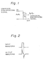
- Figure 1 shows part of a conventional horizontal synchronous separation circuit
- Fig. 2 shows input and output waveforms of the circuit shown in Fig. 1.
- the horizontal synchronous separation circuit comprises a differential circuit having a capacitor Ch and resistor Rh, and a differential time constant of this circuit is set to pass only the horizontal synchronizing signal.
- the horizontal synchronizing signal is 15.75 KHz.
- Fig. 2 when a signal having a rectangular waveform is input to the terminal IN, a signal having a differential waveform can be obtained from the terminal OUT as the horizontal synchronizing signal.
- the vertical synchronizing signal is completely cut off in this circuit.
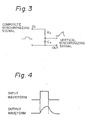
- Figure 3 shows part of a conventional vertical synchronous separation circuit
- Fig. 4 shows input and output waveforms of the circuit shown in Fig. 3.
- the vertical synchronous separation circuit comprises an integrating circuit having a resistor Rv and capacitor Cv, and an integrating time constant of this circuit is set to a value such that the horizontal synchronizing signal can be suppressed and cut off. Further, the integrating time constant is set to a value such that attenuation of the vertical synchronizing signal having a predetermined frequency (60 Hz in the NTSC method) does not occur.
- a signal having a rectangular waveform is input to the terminal IN
- a signal having an integrating waveform can be obtained from the terminal OUT.
- the waveforms of the horizontal and vertical synchronizing signals are shaped by a comparator(not shown) and used as a trigger signal for horizontal and vertical deflections.
- the horizontal synchronous separation circuit is basically constituted by the differential circuit and the vertical synchronous separation circuit is constituted by the integrating circuit, both processing the analogue signal.
- the resistors Rh, Rv and the capacitors Ch, Cv used in these circuits are passive electrical components, and accordingly, the electrical characteristics of the synchronous separation can vary considerably in accordance with the component tolerances and any changes in the components with the passage of time. For example, when the resistance value of the resistor Rh is slightly increased, the level of the differentiated horizontal synchronizing signal is lowered so that a precise horizontal synchronization cannot be obtained. Further, when the capacitance value Cv is slightly decreased, the vertical synchronization becomes unstable and it is difficult to suppress the horizontal synchronizing signal and large pulsative noise.
- these circuits should preferably be formed by integrated circuits(IC), to reduce costs, improve reliability, miniaturize the circuit, and simplify maintenance, but it is difficult to achieve the above objects with the analogue processing technique.
- IC integrated circuits
- the vertical synchronous separation circuit since the vertical synchronous frequency is very low, as explained above(60 Hz in the NTSC method), a relatively large integration time constant must be used, and this large integration time constant is difficult to realize acceptably in an integrated circuit.
- an embodiment of the present invention is designed to provide a synchronous separation circuit, for deriving separate horizontal and the vertical synchronizing signals from the composite synchronizing signal, employing digital signal processing techniques.
- CSY is the composite synchronizing signal
- CLK is the clock signal
- HSY is the horizontal synchronizing signal
- VSY is the vertical synchronizing signal.
- reference number 1 represents a synchronous separating circuit
- 2 a counting unit
- 3 a horizontal synchronous separation unit
- 4 a vertical synchronous separation unit
- 5 a clock signal generating unit.
- the synchronous separation circuit is basically constituted by the first means for generating the pulse width of the horizontal synchronizing signal, the second means for cutting off the equalizing pulse from the composite synchronizing signal, and the third means for generating the vertical synchronizing signal from the vertical synchronizing pulse of the composite synchronizing signal.
- the synchronous separation circuit 1 is constituted by; a counting unit 2 for counting pulses in a clock reference signal after detecting the leading edge of a pulse contained in the composite synchronizing signal; a horizontal synchronous separating unit 3 for providing a pulse of a fixed duration determined by counting a predetermined number of the clock pulses after detection of the said leading edge; and a vertical synchronous separating unit 4 for detecting when a pulse in the said composite synchronizing signal persists for a preset period, measured by operation of the said counting unit ( 2), and thereupon generating a vertical synchronizing pulse at an output separate from that of the said horizontal synchronizing signal.
- the unit 5 generates the clock signal as a reference signal having a frequency higher than the frequency of the horizontal synchronizing signal.
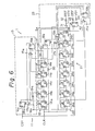
- FIG. 6 is a circuit diagram of the synchronous separation circuit according to an embodiment of the present invention. This circuit is used for separating the horizontal and vertical synchronizing signals from the composite synchronizing signal based upon the NTSC method.
- the synchronous separation circuit 1 is constituted by a counting circuit 11, a first frequency dividing counter 12, a first reset circuit 13, a supplementary counter 21, a second frequency dividing counter 22, and a second reset circuit 23.
- the first frequency dividing counter 12 and the first reset circuit 13 are contained in the counting circuit 11.
- the first frequency dividing counter 12 is constituted by a plurality of D-type flip-flop circuits(D-FF's) 14a to 14e, whose respective inverted outputs Q are fed back to the corresponding data inputs D. Accordingly, the D-FF's operate as trigger flip-flop circuits (T-FF) (divide -by-two stages) in this circuit configuration.
- the clock signal CLK is, for example, a color subcarrier Fsc (3.5795 MHz) contained in the composite video signal in the NTSC method and is input to a clock input terminal C of the D-FF 14a. Since this clock signal is used as the reference signal for the synchronization, a constant clock signal must be precisely generated. In this embodiment, the color subcarrier Fsc is utilized as the clock signal, since it is relatively stable.
- the D-FF's 14a and 14e are connected in series and operate as a counter dividing the frequency of the clock signal CLK by a factor of 32.
- the first reset circuit 13 is constituted by a NAND gate 15a having three input terminals, D-FF's 16a and 18a, and two AND gates 17a and 19a.
- the inverted output Q of the D-FF 14a, the output Q of the D-FF 14d, and the output Q of the D-FF 14e are input to corresponding input terminals of the NAND gate 15a, and the output of the NAND gate 15a is connected to the data input terminal D of the D-FF 16a.
- the clock signal CLK inverted by an inverter 20 is input to the clock input terminal of the D-FF 16a.
- the output Q of the D-FF 16a is input to one input terminal of the AND gate 17a and the power source Vcc is connected to the other input terminal of the AND gate 17a.
- the output of the AND gate 17a is input to the reset terminal R of the D-FF 18a. When the level of the reset terminal R is low, the D-FF 18a is reset and the level of the output Q becomes low.
- the composite synchronizing signal CSY having a positive polarity is input to the clock input terminal C of the D-FF 18a and the power source Vcc is connected to the data input terminal D of the D-FF 18a.
- the output Q of the D-FF 18a is input to one input terminal of the AND gate 19a, and the power source Vcc is input to the other input terminal of the AND gate 19a. Since one input terminal of each of the AND gates 17a and 19a is connected to the power source Vcc, the outputs of these gates are always identical to their respective other inputs.
- the outputs of the AND gate 19a is connected to the reset input terminal R of each of the D-FF's 14a to 14e, and when the reset input terminal R of the D-FF is low, each of the D-FF's 14a to 14e is reset and the output Q becomes low. Further, the inverted output Q becomes high.
- the first frequency dividing counter 12 starts to count from a leading edge of the clock signal CLK.
- the first frequency dividing counter 12 is reset by the first reset circuit 13. Namely, when the first frequency dividing counter 12 counts up to 24, all inputs of the NAND gate 15a become high and the output thereof becomes low.
- the low level output of the NAND gate 15a is latched to the D-FF 16a at the trailing edge of the clock signal CLK and resets the D-FF 18a through the AND gate 17a.
- each of the D-FF's 14a and 14e is reset, and when the output Q of the D-FF 18a is high, the first frequency dividing counter 12 again starts to count.
- the output Q becomes high and the first frequency dividing counter 12 starts to count.
- the counter 11 starts to count from the leading edge of the composite synchronizing signal CSY. When the counter 11 counts up to 24, the counter 11 is reset and stops counting until the leading edge of the next composite synchronizing signal appears.
- the supplementary counter 21 is constituted by the second frequency dividing counter 22 and the second reset counter 23.
- the second frequency dividing counter 22 is constituted by the D-type flip-flop(D-FF's) circuits 24a to 24h.
- the inversion output Q of each of the D-FF's 24a to 24h is fed back to its own data input terminal D. Accordingly, each D-FF operates as a T-Type flip-flop(T-FF) circuit.
- the clock signal CLK is input to the clock input terminal C of the D-FF's 24a to 24h connected in series, and accordingly, the second frequency dividing counter 22 operates as a counter dividing the clock signal frequency by 256.
- the second reset circuit 23 has the same structure as the first reset circuit 13, and accordingly, 15b represents a NAND gate, 16b and 18b represent D-FF's, and 17b and 19b represent AND gates.
- the second frequency dividing circuit 22 is reset by the second reset circuit 23 when all inputs of the AND gate 15b become high.
- the inversion output Q of the D-FF 24a, the output Q of the D-FF 24g, and the output Q of the D-FF 24h are connected to the input terminals of the AND gate 15b, and accordingly, when the second frequency dividing circuit 22 counts up to 192, the D-FF's 24a to 24h are reset.
- the second frequency dividing circuit 22 starts to count.
- the output of the counter 11 i.e., the output Q of the D-FF 14e
- the data input D of the D-FF 18b is latched to the high level and the second frequency dividing circuit 22 starts to count.
- the second frequency dividing circuit 22 starts to count on the leading edge of the output signal of the counter 11, and when the second frequency dividing circuit 22 has counted the clock signal up to 192, it is reset and stops counting the clock signal until the leading edge of the next output pulse of the counter 11 arrives.
- the outputs of the counter 11 and the supplementary counter 21(inverted output Q of the D-FF 24h) are input to the NAND gate 31.
- the output of the NAND gate 31 is the horizontal synchronizing signal HSY, and the inverted output HSY is obtained through the inverter 32.
- the supplementary counter 21 and the NAND gate 31 have the horizontal synchronous separation function.
- the outputs of the D-FF's 14d and 14e in the first frequency dividing counter 12 are input to the NAND gate 41, and the output of the NAND gate 41 is input to the clock input terminal C of the D-FF 42.
- the reset input terminal R of the D-FF 42 is connected to the power source Vcc.
- the composite synchronizing signal CSY is input to the data input terminal D of the D-FF 42; the output Q and the inversion output Q of the D-FF 42 are connected to the input terminals of the inverters 43 and 44, and the outputs of the inverters 43 and 44 are the vertical synchronizing signals VSY and the inversion signal VSY.
- the NAND gate 41 and the D-FF 42 have the vertical synchronous separation function.
- Figure 7 is a signal timing chart for explaining the operation of the circuit shown in Fig. 6.
- CSY is the composite synchronizing signal
- S11 is the output of the counter 11
- S21 is the output of the supplementary counter 21
- HSY is the horizontal synchronizing signal
- S41 is the output of the NAND gate 41
- VSY is the vertical synchronizing signal.
- the signal timing of the composite synchronizing signal is already defined in detail in the NTSC method.
- the pulse width of the horizontal synchronizing signal is 0.075 H
- the pulse width of the cutting pulse(groove between the vertical synchronous phase) is 0.07 H
- the pulse width of the equalizing pulse is 0.4 H.
- each period of the pulse train formed by the horizontal synchronizing signal, the cutting pulse and the equalizing pulse in the vertical blanking term is also defined by 0.5 H from the front edge of each pulse.
- the counter starts to count reference signal clock pulses (having a frequency higher than that of the horizontal synchronizing signal) on detecting the leading edge of the composite synchronizing signal, it is possible to determine the respective positions of the horizontal synchronizing signal, the vertical synchronizing signal, and the supplementary pulse in terms of the count number.
- the first frequency dividing counter 12 When the composite synchronizing signal CSY is applied to the first reset circuit 13 in the counter 11, the first frequency dividing counter 12 is released from the reset state by the first reset circuit 13 at the leading edge of the composite synchronizing signal CSY, and the first frequency dividing counter 12 starts to count the composite synchronizing signal.
- the first frequency dividing counter 12 When the first frequency dividing counter 12 has counted twenty-four pulses in the clock signal CLK, the first frequency dividing counter 12 is reset. The first frequency dividing counter 12 is then triggered again, to count 24 clock cycles, on the leading edge of the next pulse contained in the composite synchronizing signal CSY. At that time, the count of the counter 11 corresponds to 24 clock cycles of the clock signal CLK, and this value is approximately 0.1H. Accordingly, the horizontal synchronizing signal and the supplementary pulse, each of duration 0.1H, are regenerated in an inverted form as the signal S11 at the output of the counter 11 as shown in Fig. 7.
- the second frequency dividing counter 22 operates in the same way as the first frequency dividing counter 12.
- the second frequency dividing counter 22 is reset after a count of 192. Since the second frequency dividing counter 22 starts to count from the leading edge of the signal S11, the output S21 of the supplementary counter 21 is reset when a count of 192 is reached after the detection of that leading edge. Since the leading edge of the signal S21 is synchronized with the trailing edge of the horizontal synchronizing signal and, the pulse width of the signal S21 is 192 clock cycles(0.86 H), the equalizing pulse and the cutting pulse occur while the signal S21 is high. Therefore, when the signal S11 and S21 are applied to the NAND gate 31, only the horizontal synchronizing signal HSY is output from the NAND gate 31.
- the supplementary counter 21 starts to count from the leading edge of the signal S11, in the event of a loss of synchronism the count may be initiated by the supplementary pulse.
- the second frequency dividing counter 22 will not stop counting until a count of 196 is reached, the counting operation will not have been completed before the next horizontal synchronizing signal appears.
- the counter starts to count from the leading edge of the horizontal synchronizing signal, so that normal operation is restored after the above operation.
- the output S41 of the NAND gate 41 triggers the D-FF 42 when the inverted output Q of each of the D-FF's 14d and 14e is low. Namely, the signal S41 becomes high at only half a cycle of the clock signal CLK just before the trailing edge of the horizontal synchronizing signal HSY provided by the NAND gate 31. At that time, since the pulse width of the signal S11 is 0.1 H, the horizontal synchronizing pulse, equalizing pulse, and cutting pulse contained in the composite synchronizing signal do not occur at the instant at which the signal S41 becomes high.
- the horizontal synchronizing signal and the vertical synchronizing signal are generated using digital signal processing techniques, without using a differential circuit and an integrating circuit, and accordingly, the IC circuit can be easily and inexpensively manufactured, the reliability improved, the circuit miniaturized, and maintenance simplified.
- asynchronous type counter is provided for the first and second counters 12 and 22, a synchronous type counter can be used instead.
- the counter 11 and the supplementary counter 21 are independently provided in the synchronous separation circuit, the output of the D-FF's 24d and 24e of the supplementary counter 21 can be utilized, and in this case, only one counter need be provided in the synchronous separation circuit, and thus the costs are reduced and the integration circuit is further miniaturized.
- the color subcarrier Fsc is used as the clock signal CLK in this embodiment, an oscillator can be provided for generating the clock signal CLK, and in this case, the frequency of the clock signal is set to a value higher than that of the horizontal synchronizing signal.
Landscapes
- Engineering & Computer Science (AREA)
- Multimedia (AREA)
- Signal Processing (AREA)
- Synchronizing For Television (AREA)
Applications Claiming Priority (2)
| Application Number | Priority Date | Filing Date | Title |
|---|---|---|---|
| JP63013116A JPH01189284A (ja) | 1988-01-22 | 1988-01-22 | 同期分離回路 |
| JP13116/88 | 1988-01-22 |
Publications (3)
| Publication Number | Publication Date |
|---|---|
| EP0327228A2 true EP0327228A2 (fr) | 1989-08-09 |
| EP0327228A3 EP0327228A3 (en) | 1990-12-05 |
| EP0327228B1 EP0327228B1 (fr) | 1995-03-29 |
Family
ID=11824182
Family Applications (1)
| Application Number | Title | Priority Date | Filing Date |
|---|---|---|---|
| EP89300578A Expired - Lifetime EP0327228B1 (fr) | 1988-01-22 | 1989-01-20 | Circuit de séparation d'impulsion de synchronisation |
Country Status (5)
| Country | Link |
|---|---|
| US (1) | US4999708A (fr) |
| EP (1) | EP0327228B1 (fr) |
| JP (1) | JPH01189284A (fr) |
| KR (1) | KR920001286B1 (fr) |
| DE (1) | DE68921904T2 (fr) |
Families Citing this family (9)
| Publication number | Priority date | Publication date | Assignee | Title |
|---|---|---|---|---|
| IT1236913B (it) * | 1989-12-21 | 1993-04-26 | Sgs Thomson Microelectronics | Metodo di misura automatica della frequenza di scansione orizzontale di un segnale a sincronismo composito e circuito elettronico operante secondo detto metodo |
| USRE36508E (en) * | 1989-12-21 | 2000-01-18 | Sgs-Thomson Microelectronics S.R.L. | Method of automatically measuring the horizontal scan frequency of a composite synchronism signal, and an electronic circuit operating in accordance with the method |
| JPH0769670B2 (ja) * | 1990-08-03 | 1995-07-31 | インターナシヨナル・ビジネス・マシーンズ・コーポレーション | 電源装置 |
| JPH05260345A (ja) * | 1992-03-12 | 1993-10-08 | Mitsubishi Electric Corp | 複合同期信号分離回路 |
| WO1998030102A1 (fr) * | 1997-01-09 | 1998-07-16 | Emory University | Metalloporphyrines non-ferreuses et procedes d'utilisation |
| US5999222A (en) * | 1997-09-04 | 1999-12-07 | Hughes-Jvc Technology Corporation | Digital vertical sync separator |
| KR100304891B1 (ko) * | 1998-12-31 | 2001-09-24 | 구자홍 | 평판형 표시장치 시스템 |
| JP4110839B2 (ja) | 2002-05-31 | 2008-07-02 | ソニー株式会社 | 表示装置および携帯端末 |
| KR20060009597A (ko) * | 2004-07-26 | 2006-02-01 | 삼성전자주식회사 | 영상신호 합성방법, 영상신호 합성장치, 디스플레이시스템, 디스플레이장치 및 디스플레이장치의 제어방법 |
Family Cites Families (6)
| Publication number | Priority date | Publication date | Assignee | Title |
|---|---|---|---|---|
| US4491870A (en) * | 1982-08-17 | 1985-01-01 | Rca Corporation | Digital sync separator |
| JPS60113585A (ja) * | 1983-11-24 | 1985-06-20 | Citizen Watch Co Ltd | 同期信号発生回路 |
| US4769704A (en) * | 1985-06-04 | 1988-09-06 | Matsushita Electric Industrial Co., Ltd. | Synchronization signal generator |
| US4675734A (en) * | 1985-06-06 | 1987-06-23 | Polaroid Corporation | Sync pulse separator circuit |
| JPH06101804B2 (ja) * | 1985-09-25 | 1994-12-12 | ヤマハ株式会社 | 垂直同期タイミング信号発生回路 |
| JPS62171281A (ja) * | 1986-01-23 | 1987-07-28 | Mitsubishi Electric Corp | 垂直同期信号分離回路 |
-
1988
- 1988-01-22 JP JP63013116A patent/JPH01189284A/ja active Pending
-
1989
- 1989-01-20 DE DE68921904T patent/DE68921904T2/de not_active Expired - Fee Related
- 1989-01-20 EP EP89300578A patent/EP0327228B1/fr not_active Expired - Lifetime
- 1989-01-21 KR KR8900631A patent/KR920001286B1/ko not_active Expired
- 1989-01-23 US US07/299,534 patent/US4999708A/en not_active Expired - Fee Related
Also Published As
| Publication number | Publication date |
|---|---|
| DE68921904T2 (de) | 1995-07-27 |
| US4999708A (en) | 1991-03-12 |
| DE68921904D1 (de) | 1995-05-04 |
| KR920001286B1 (en) | 1992-02-10 |
| JPH01189284A (ja) | 1989-07-28 |
| EP0327228A3 (en) | 1990-12-05 |
| EP0327228B1 (fr) | 1995-03-29 |
| KR890012482A (ko) | 1989-08-26 |
Similar Documents
| Publication | Publication Date | Title |
|---|---|---|
| JPH02143688A (ja) | 異種ビデオ・フォーマット識別装置 | |
| EP0327228A2 (fr) | Circuit de séparation d'impulsion de synchronisation | |
| US4763341A (en) | Digital timing using a state machine | |
| US4491870A (en) | Digital sync separator | |
| JPH0644818B2 (ja) | 表示装置 | |
| KR950007417A (ko) | 디지탈 수직동기신호 분리장치 | |
| JPH0411410Y2 (fr) | ||
| KR930011431B1 (ko) | 표준 영상신호를 위한 동기신호 재발생회로 | |
| KR920001109B1 (ko) | Vdp정지신호 검출회로 | |
| JP2789616B2 (ja) | 垂直自動同期回路 | |
| JP2642242B2 (ja) | パイロットバーストゲートパルス発生装置 | |
| KR0180617B1 (ko) | 필드판별회로 | |
| KR0160119B1 (ko) | 블랭킹신호 및 필드구별신호 검출회로 | |
| JP3253451B2 (ja) | コンポジット同期信号の遅延回路 | |
| KR0169372B1 (ko) | 필드신호 검출장치 | |
| JP2577359B2 (ja) | 垂直同期信号の周波数判別回路 | |
| JPS59110280A (ja) | 水平同期信号処理回路 | |
| KR950012248B1 (ko) | 텔레비젼 수상기의 배속 동기신호 발생 시스템 | |
| US5548191A (en) | Vertical deflection circuit for a television receiver | |
| JPS62207078A (ja) | ミユ−テイング回路 | |
| JPS62108676A (ja) | 水平同期信号ブランキングパルス発生器 | |
| JPS63173467A (ja) | 水平同期信号ブランキングパルス発生器 | |
| JPH04229778A (ja) | 垂直同期信号分離回路 | |
| JPH0416990B2 (fr) | ||
| JPH0636561B2 (ja) | 水平同期信号分離装置 |
Legal Events
| Date | Code | Title | Description |
|---|---|---|---|
| PUAI | Public reference made under article 153(3) epc to a published international application that has entered the european phase |
Free format text: ORIGINAL CODE: 0009012 |
|
| AK | Designated contracting states |
Kind code of ref document: A2 Designated state(s): DE FR GB |
|
| PUAL | Search report despatched |
Free format text: ORIGINAL CODE: 0009013 |
|
| AK | Designated contracting states |
Kind code of ref document: A3 Designated state(s): DE FR GB |
|
| 17P | Request for examination filed |
Effective date: 19901228 |
|
| 17Q | First examination report despatched |
Effective date: 19930202 |
|
| GRAA | (expected) grant |
Free format text: ORIGINAL CODE: 0009210 |
|
| AK | Designated contracting states |
Kind code of ref document: B1 Designated state(s): DE FR GB |
|
| REF | Corresponds to: |
Ref document number: 68921904 Country of ref document: DE Date of ref document: 19950504 |
|
| ET | Fr: translation filed | ||
| PG25 | Lapsed in a contracting state [announced via postgrant information from national office to epo] |
Ref country code: GB Effective date: 19960120 |
|
| PLBE | No opposition filed within time limit |
Free format text: ORIGINAL CODE: 0009261 |
|
| STAA | Information on the status of an ep patent application or granted ep patent |
Free format text: STATUS: NO OPPOSITION FILED WITHIN TIME LIMIT |
|
| 26N | No opposition filed | ||
| GBPC | Gb: european patent ceased through non-payment of renewal fee |
Effective date: 19960120 |
|
| PGFP | Annual fee paid to national office [announced via postgrant information from national office to epo] |
Ref country code: DE Payment date: 20010115 Year of fee payment: 13 |
|
| PGFP | Annual fee paid to national office [announced via postgrant information from national office to epo] |
Ref country code: FR Payment date: 20010125 Year of fee payment: 13 |
|
| PG25 | Lapsed in a contracting state [announced via postgrant information from national office to epo] |
Ref country code: DE Free format text: LAPSE BECAUSE OF NON-PAYMENT OF DUE FEES Effective date: 20020801 |
|
| PG25 | Lapsed in a contracting state [announced via postgrant information from national office to epo] |
Ref country code: FR Free format text: LAPSE BECAUSE OF NON-PAYMENT OF DUE FEES Effective date: 20020930 |
|
| REG | Reference to a national code |
Ref country code: FR Ref legal event code: ST |