EP0327406A2 - Plasmabearbeitungsmethode und Vorrichtung zum Aufbringen von Dünnschichten - Google Patents
Plasmabearbeitungsmethode und Vorrichtung zum Aufbringen von Dünnschichten Download PDFInfo
- Publication number
- EP0327406A2 EP0327406A2 EP89301126A EP89301126A EP0327406A2 EP 0327406 A2 EP0327406 A2 EP 0327406A2 EP 89301126 A EP89301126 A EP 89301126A EP 89301126 A EP89301126 A EP 89301126A EP 0327406 A2 EP0327406 A2 EP 0327406A2
- Authority
- EP
- European Patent Office
- Prior art keywords
- plasma
- substrate
- high frequency
- electrical energy
- reaction
- Prior art date
- Legal status (The legal status is an assumption and is not a legal conclusion. Google has not performed a legal analysis and makes no representation as to the accuracy of the status listed.)
- Granted
Links
- 230000008021 deposition Effects 0.000 title claims abstract description 30
- 238000003672 processing method Methods 0.000 title claims description 6
- 239000010409 thin film Substances 0.000 title description 4
- 239000000758 substrate Substances 0.000 claims abstract description 72
- 229910052799 carbon Inorganic materials 0.000 claims abstract description 54
- OKTJSMMVPCPJKN-UHFFFAOYSA-N Carbon Chemical compound [C] OKTJSMMVPCPJKN-UHFFFAOYSA-N 0.000 claims abstract description 52
- 238000006243 chemical reaction Methods 0.000 claims abstract description 42
- 238000000151 deposition Methods 0.000 claims abstract description 32
- 238000000034 method Methods 0.000 claims abstract description 23
- 238000005530 etching Methods 0.000 claims abstract description 17
- 238000004544 sputter deposition Methods 0.000 claims abstract description 10
- 230000000694 effects Effects 0.000 claims description 8
- 230000001939 inductive effect Effects 0.000 claims description 5
- 238000003486 chemical etching Methods 0.000 claims description 2
- 238000005229 chemical vapour deposition Methods 0.000 claims description 2
- 230000005684 electric field Effects 0.000 abstract description 3
- 239000012495 reaction gas Substances 0.000 abstract 1
- 239000010408 film Substances 0.000 description 66
- 239000007789 gas Substances 0.000 description 35
- 230000000737 periodic effect Effects 0.000 description 13
- 239000011521 glass Substances 0.000 description 11
- 238000000576 coating method Methods 0.000 description 8
- VYPSYNLAJGMNEJ-UHFFFAOYSA-N Silicium dioxide Chemical compound O=[Si]=O VYPSYNLAJGMNEJ-UHFFFAOYSA-N 0.000 description 7
- 229910052782 aluminium Inorganic materials 0.000 description 7
- 239000011248 coating agent Substances 0.000 description 7
- HSFWRNGVRCDJHI-UHFFFAOYSA-N Acetylene Chemical compound C#C HSFWRNGVRCDJHI-UHFFFAOYSA-N 0.000 description 6
- IJGRMHOSHXDMSA-UHFFFAOYSA-N Atomic nitrogen Chemical compound N#N IJGRMHOSHXDMSA-UHFFFAOYSA-N 0.000 description 6
- 239000004411 aluminium Substances 0.000 description 6
- XAGFODPZIPBFFR-UHFFFAOYSA-N aluminium Chemical compound [Al] XAGFODPZIPBFFR-UHFFFAOYSA-N 0.000 description 6
- 239000001257 hydrogen Substances 0.000 description 6
- 229910052739 hydrogen Inorganic materials 0.000 description 6
- 230000004048 modification Effects 0.000 description 6
- 238000012986 modification Methods 0.000 description 6
- 229920002120 photoresistant polymer Polymers 0.000 description 6
- YCKRFDGAMUMZLT-UHFFFAOYSA-N Fluorine atom Chemical compound [F] YCKRFDGAMUMZLT-UHFFFAOYSA-N 0.000 description 5
- UFHFLCQGNIYNRP-UHFFFAOYSA-N Hydrogen Chemical compound [H][H] UFHFLCQGNIYNRP-UHFFFAOYSA-N 0.000 description 5
- 125000004429 atom Chemical group 0.000 description 5
- 230000000903 blocking effect Effects 0.000 description 5
- 238000010586 diagram Methods 0.000 description 5
- 239000011737 fluorine Substances 0.000 description 5
- 229910052731 fluorine Inorganic materials 0.000 description 5
- 239000004065 semiconductor Substances 0.000 description 5
- 229910052814 silicon oxide Inorganic materials 0.000 description 5
- 229910003460 diamond Inorganic materials 0.000 description 4
- 239000010432 diamond Substances 0.000 description 4
- OAICVXFJPJFONN-UHFFFAOYSA-N Phosphorus Chemical compound [P] OAICVXFJPJFONN-UHFFFAOYSA-N 0.000 description 3
- 229910052581 Si3N4 Inorganic materials 0.000 description 3
- QVGXLLKOCUKJST-UHFFFAOYSA-N atomic oxygen Chemical compound [O] QVGXLLKOCUKJST-UHFFFAOYSA-N 0.000 description 3
- 230000015572 biosynthetic process Effects 0.000 description 3
- 239000000919 ceramic Substances 0.000 description 3
- 239000012535 impurity Substances 0.000 description 3
- 239000000463 material Substances 0.000 description 3
- 229910052757 nitrogen Inorganic materials 0.000 description 3
- 239000001301 oxygen Substances 0.000 description 3
- 229910052760 oxygen Inorganic materials 0.000 description 3
- 229910052698 phosphorus Inorganic materials 0.000 description 3
- 239000011574 phosphorus Substances 0.000 description 3
- 238000001020 plasma etching Methods 0.000 description 3
- HQVNEWCFYHHQES-UHFFFAOYSA-N silicon nitride Chemical group N12[Si]34N5[Si]62N3[Si]51N64 HQVNEWCFYHHQES-UHFFFAOYSA-N 0.000 description 3
- XKRFYHLGVUSROY-UHFFFAOYSA-N Argon Chemical compound [Ar] XKRFYHLGVUSROY-UHFFFAOYSA-N 0.000 description 2
- ZOXJGFHDIHLPTG-UHFFFAOYSA-N Boron Chemical compound [B] ZOXJGFHDIHLPTG-UHFFFAOYSA-N 0.000 description 2
- 229910052796 boron Inorganic materials 0.000 description 2
- 239000002019 doping agent Substances 0.000 description 2
- 230000009977 dual effect Effects 0.000 description 2
- 125000000219 ethylidene group Chemical group [H]C(=[*])C([H])([H])[H] 0.000 description 2
- 238000002347 injection Methods 0.000 description 2
- 239000007924 injection Substances 0.000 description 2
- 238000004519 manufacturing process Methods 0.000 description 2
- VNWKTOKETHGBQD-UHFFFAOYSA-N methane Chemical compound C VNWKTOKETHGBQD-UHFFFAOYSA-N 0.000 description 2
- 239000005020 polyethylene terephthalate Substances 0.000 description 2
- 229920000139 polyethylene terephthalate Polymers 0.000 description 2
- 229910052710 silicon Inorganic materials 0.000 description 2
- 239000000126 substance Substances 0.000 description 2
- 241000272194 Ciconiiformes Species 0.000 description 1
- MYMOFIZGZYHOMD-UHFFFAOYSA-N Dioxygen Chemical compound O=O MYMOFIZGZYHOMD-UHFFFAOYSA-N 0.000 description 1
- 239000004593 Epoxy Substances 0.000 description 1
- LFQSCWFLJHTTHZ-UHFFFAOYSA-N Ethanol Chemical compound CCO LFQSCWFLJHTTHZ-UHFFFAOYSA-N 0.000 description 1
- VGGSQFUCUMXWEO-UHFFFAOYSA-N Ethene Chemical compound C=C VGGSQFUCUMXWEO-UHFFFAOYSA-N 0.000 description 1
- 239000005977 Ethylene Substances 0.000 description 1
- KRHYYFGTRYWZRS-UHFFFAOYSA-M Fluoride anion Chemical compound [F-] KRHYYFGTRYWZRS-UHFFFAOYSA-M 0.000 description 1
- OKKJLVBELUTLKV-UHFFFAOYSA-N Methanol Chemical compound OC OKKJLVBELUTLKV-UHFFFAOYSA-N 0.000 description 1
- 239000004642 Polyimide Substances 0.000 description 1
- XUIMIQQOPSSXEZ-UHFFFAOYSA-N Silicon Chemical compound [Si] XUIMIQQOPSSXEZ-UHFFFAOYSA-N 0.000 description 1
- 239000005030 aluminium foil Substances 0.000 description 1
- 229910003481 amorphous carbon Inorganic materials 0.000 description 1
- 229910052787 antimony Inorganic materials 0.000 description 1
- 229910052786 argon Inorganic materials 0.000 description 1
- 229910052785 arsenic Inorganic materials 0.000 description 1
- 238000005513 bias potential Methods 0.000 description 1
- 230000005540 biological transmission Effects 0.000 description 1
- 229910052797 bismuth Inorganic materials 0.000 description 1
- 150000001722 carbon compounds Chemical class 0.000 description 1
- 229910052681 coesite Inorganic materials 0.000 description 1
- 239000004020 conductor Substances 0.000 description 1
- 239000000356 contaminant Substances 0.000 description 1
- 229910052906 cristobalite Inorganic materials 0.000 description 1
- 238000005137 deposition process Methods 0.000 description 1
- 238000009792 diffusion process Methods 0.000 description 1
- 229910001882 dioxygen Inorganic materials 0.000 description 1
- 230000035622 drinking Effects 0.000 description 1
- 239000000428 dust Substances 0.000 description 1
- 235000019441 ethanol Nutrition 0.000 description 1
- 230000005284 excitation Effects 0.000 description 1
- 238000002474 experimental method Methods 0.000 description 1
- 229910052736 halogen Inorganic materials 0.000 description 1
- 150000002367 halogens Chemical class 0.000 description 1
- 229910021385 hard carbon Inorganic materials 0.000 description 1
- 238000010438 heat treatment Methods 0.000 description 1
- 150000002431 hydrogen Chemical class 0.000 description 1
- 230000001788 irregular Effects 0.000 description 1
- 230000000873 masking effect Effects 0.000 description 1
- 239000013081 microcrystal Substances 0.000 description 1
- 239000000203 mixture Substances 0.000 description 1
- 150000002927 oxygen compounds Chemical class 0.000 description 1
- 239000002245 particle Substances 0.000 description 1
- 239000005360 phosphosilicate glass Substances 0.000 description 1
- 238000005268 plasma chemical vapour deposition Methods 0.000 description 1
- 239000004033 plastic Substances 0.000 description 1
- 229920003023 plastic Polymers 0.000 description 1
- 229920003229 poly(methyl methacrylate) Polymers 0.000 description 1
- 229920001721 polyimide Polymers 0.000 description 1
- 239000004926 polymethyl methacrylate Substances 0.000 description 1
- 229910052761 rare earth metal Inorganic materials 0.000 description 1
- 239000011347 resin Substances 0.000 description 1
- 229920005989 resin Polymers 0.000 description 1
- 239000010703 silicon Substances 0.000 description 1
- 239000000377 silicon dioxide Substances 0.000 description 1
- 235000012239 silicon dioxide Nutrition 0.000 description 1
- 229910052709 silver Inorganic materials 0.000 description 1
- 229910001220 stainless steel Inorganic materials 0.000 description 1
- 239000010935 stainless steel Substances 0.000 description 1
- 229910052682 stishovite Inorganic materials 0.000 description 1
- -1 tefon Substances 0.000 description 1
- 229910052905 tridymite Inorganic materials 0.000 description 1
- 238000009827 uniform distribution Methods 0.000 description 1
Images




Classifications
-
- C—CHEMISTRY; METALLURGY
- C23—COATING METALLIC MATERIAL; COATING MATERIAL WITH METALLIC MATERIAL; CHEMICAL SURFACE TREATMENT; DIFFUSION TREATMENT OF METALLIC MATERIAL; COATING BY VACUUM EVAPORATION, BY SPUTTERING, BY ION IMPLANTATION OR BY CHEMICAL VAPOUR DEPOSITION, IN GENERAL; INHIBITING CORROSION OF METALLIC MATERIAL OR INCRUSTATION IN GENERAL
- C23C—COATING METALLIC MATERIAL; COATING MATERIAL WITH METALLIC MATERIAL; SURFACE TREATMENT OF METALLIC MATERIAL BY DIFFUSION INTO THE SURFACE, BY CHEMICAL CONVERSION OR SUBSTITUTION; COATING BY VACUUM EVAPORATION, BY SPUTTERING, BY ION IMPLANTATION OR BY CHEMICAL VAPOUR DEPOSITION, IN GENERAL
- C23C16/00—Chemical coating by decomposition of gaseous compounds, without leaving reaction products of surface material in the coating, i.e. chemical vapour deposition [CVD] processes
- C23C16/22—Chemical coating by decomposition of gaseous compounds, without leaving reaction products of surface material in the coating, i.e. chemical vapour deposition [CVD] processes characterised by the deposition of inorganic material, other than metallic material
- C23C16/26—Deposition of carbon only
-
- H—ELECTRICITY
- H01—ELECTRIC ELEMENTS
- H01J—ELECTRIC DISCHARGE TUBES OR DISCHARGE LAMPS
- H01J37/00—Discharge tubes with provision for introducing objects or material to be exposed to the discharge, e.g. for the purpose of examination or processing thereof
- H01J37/32—Gas-filled discharge tubes
- H01J37/32009—Arrangements for generation of plasma specially adapted for examination or treatment of objects, e.g. plasma sources
- H01J37/32082—Radio frequency generated discharge
-
- C—CHEMISTRY; METALLURGY
- C23—COATING METALLIC MATERIAL; COATING MATERIAL WITH METALLIC MATERIAL; CHEMICAL SURFACE TREATMENT; DIFFUSION TREATMENT OF METALLIC MATERIAL; COATING BY VACUUM EVAPORATION, BY SPUTTERING, BY ION IMPLANTATION OR BY CHEMICAL VAPOUR DEPOSITION, IN GENERAL; INHIBITING CORROSION OF METALLIC MATERIAL OR INCRUSTATION IN GENERAL
- C23C—COATING METALLIC MATERIAL; COATING MATERIAL WITH METALLIC MATERIAL; SURFACE TREATMENT OF METALLIC MATERIAL BY DIFFUSION INTO THE SURFACE, BY CHEMICAL CONVERSION OR SUBSTITUTION; COATING BY VACUUM EVAPORATION, BY SPUTTERING, BY ION IMPLANTATION OR BY CHEMICAL VAPOUR DEPOSITION, IN GENERAL
- C23C16/00—Chemical coating by decomposition of gaseous compounds, without leaving reaction products of surface material in the coating, i.e. chemical vapour deposition [CVD] processes
- C23C16/44—Chemical coating by decomposition of gaseous compounds, without leaving reaction products of surface material in the coating, i.e. chemical vapour deposition [CVD] processes characterised by the method of coating
- C23C16/50—Chemical coating by decomposition of gaseous compounds, without leaving reaction products of surface material in the coating, i.e. chemical vapour deposition [CVD] processes characterised by the method of coating using electric discharges
- C23C16/517—Chemical coating by decomposition of gaseous compounds, without leaving reaction products of surface material in the coating, i.e. chemical vapour deposition [CVD] processes characterised by the method of coating using electric discharges using a combination of discharges covered by two or more of groups C23C16/503 - C23C16/515
-
- H—ELECTRICITY
- H01—ELECTRIC ELEMENTS
- H01J—ELECTRIC DISCHARGE TUBES OR DISCHARGE LAMPS
- H01J37/00—Discharge tubes with provision for introducing objects or material to be exposed to the discharge, e.g. for the purpose of examination or processing thereof
- H01J37/32—Gas-filled discharge tubes
- H01J37/32009—Arrangements for generation of plasma specially adapted for examination or treatment of objects, e.g. plasma sources
- H01J37/32082—Radio frequency generated discharge
- H01J37/32137—Radio frequency generated discharge controlling of the discharge by modulation of energy
- H01J37/32155—Frequency modulation
- H01J37/32165—Plural frequencies
-
- H—ELECTRICITY
- H01—ELECTRIC ELEMENTS
- H01J—ELECTRIC DISCHARGE TUBES OR DISCHARGE LAMPS
- H01J37/00—Discharge tubes with provision for introducing objects or material to be exposed to the discharge, e.g. for the purpose of examination or processing thereof
- H01J37/32—Gas-filled discharge tubes
- H01J37/32431—Constructional details of the reactor
- H01J37/32532—Electrodes
- H01J37/32568—Relative arrangement or disposition of electrodes; moving means
-
- H—ELECTRICITY
- H01—ELECTRIC ELEMENTS
- H01J—ELECTRIC DISCHARGE TUBES OR DISCHARGE LAMPS
- H01J37/00—Discharge tubes with provision for introducing objects or material to be exposed to the discharge, e.g. for the purpose of examination or processing thereof
- H01J37/32—Gas-filled discharge tubes
- H01J37/34—Gas-filled discharge tubes operating with cathodic sputtering
-
- H—ELECTRICITY
- H01—ELECTRIC ELEMENTS
- H01J—ELECTRIC DISCHARGE TUBES OR DISCHARGE LAMPS
- H01J2237/00—Discharge tubes exposing object to beam, e.g. for analysis treatment, etching, imaging
- H01J2237/32—Processing objects by plasma generation
- H01J2237/33—Processing objects by plasma generation characterised by the type of processing
- H01J2237/332—Coating
- H01J2237/3321—CVD [Chemical Vapor Deposition]
Definitions
- the present invention relates to plasma processing method and apparatus for the deposition of thin films.
- a plasma processing method comprising disposing at least one substrate in a reaction space; supplying a reactive gas to said reaction space; inducing a plasma in said reaction space by applying high frequency electrical energy to said reactive gas; and performing a plasma state reaction on the surface of said substrate; and wherein alternating electrical energy, at a frequency lower than that of said plasma inducing high frequency electrical energy, is applied to said substrate during the plasma state reaction in order to initiate sputtering on said substrate.
- a plasma processing apparatus comprising a reaction chamber; a gas supply system for introducing reactive gas into said reaction chamber; a vacuum pump for evacuating said reaction chamber and maintaining a suitable gas pressure in said reaction chamber; first and second electrodes between which a plasma generating space is defined; a substrate holder for supporting at least one substrate in said plasma generating space; a high frequency power supply for supplying high frequency power to the electrodes; and an alternating power supply for applying an alternating voltage to said substrate holder, the frequency of the alternating voltage being such that a substrate supported by said substrate holder will be substantially subjected to sputtering action of the plasma generated in the plasma generating space.
- the present invention provides a chemical vapour deposition or etching method or apparatus in which a high energy plasma is established in a reaction chamber containing a reactive gas in order to effect deposition of a component of said reactive gas upon a substrate or in order to effect etching, respectively, and wherein electrical conditions are furthermore established in said chamber so as to induce sputtering to said substrate.
- a plasma of reactive gas is created between a pair of electrodes to which high frequency electrical energy is supplied, and a number of substrates are disposed within the plasma space and subjected to an alternating electric field.
- Glow discharge takes place by virtue of the application of high frequency power between the pair of electrodes and, by virtue of the alternating voltage supplied to the substrates, sputtering is effected thereto.
- the sputtering action has two functions, namely during deposition it enables amorphous films to be deposited, and during etching it increases the etching speed.
- Carbon films can for example be deposited in accordance with the teachings of the present invention in the form of so-called diamond-like carbon whose Vickers hardness might be expected to be 6500 Kg/mm2 or higher depending on the formation conditions and whose energy gap is not lower than 1.0 eV and more preferably will be in the region of 1.5 to 5.5 eV.
- the smooth and hard surface of such carbon films is very advantageous.
- the high thermal conductivity of such carbon films makes it more readily possible to dissipate the heat that is generated in operation of the integrated circuit or semiconductor device and thereby avoid problems associated with high temperature. It is also possible to fabricate carbon films containing diamond particles by adjusting the deposition conditions and such films are useful for their abrasive properties.
- Phosphorus or diborane for example may be introduced into the plasma with a carbon containing reactive gas in order to make the deposited film semiconductive.
- the reaction chamber may be cleaned by effecting plasma etching with argon for example by the plasma process in accordance with the present invention.
- FIG. 1 this is a schematic showing of a plasma CVD apparatus in accordance with the present invention for use in depositing carbon films for example.
- the apparatus comprises a loading and unloading chamber 7′, a reaction chamber 7 connected to the loading chamber 7′ through a gate valve 9, a vacuum system provided for evacuating the reaction chamber 7 and consisting of a pressure control valve 21, a turbo molecular pump 22 and a rotary pump 23, a gas feeding system 10 for introducing process gases into the reaction chamber 7 through nozzle 25, a substrate holder 1′ functioning also as an electrode, a pair of mesh or grid electrodes 3 and 3′, and a high frequency electric energy supply 40 connected with the substrate holder 1′ and the mesh electrodes 3 and 3′ and consisting of a high frequency power source 15, a matching transformer 16, an AC power source 17 and bias applying means 29.
- a temperature controlling means is provided in the chamber 7 in order to maintain the temperature of the reactive gas, between 450°C and -100°C for example, although not illustrated in the figure.
- the output frequency of the high frequency power source 15 is from 1 to 50 MHz, e.g. 13.56 MHz.
- the pair of electrodes 3 and 3′ are connected respectively to the ends 4 and 4′ of the secondary coil of the transformer 16.
- the substrate holder 1′ is electrically connected to the midpoint of the secondary coil through the AC power source 17 and the bias applying means 29.
- the frequency of the AC source is from 1 to 500 KHz, e.g. 50 KHz.
- the plasma generating space between the electrodes 3 and 3′ is confined by an enclosure 2 whose upper and lower openings are closed by a pair of lids 8 and 8′.
- the enclosure is a four-sided rectangle of 20 cm to 1 m height and 30 cm to 3 m width.
- a microwave excitation device 26 may be provided in association with the gas feeding system 10, the device 25 serving to energise the reactive gas supplied from the gas feeding system 10 by subjecting it to microwave energy, at for example, 2.45 GHz and from 200W to 2KW.
- microwave energy at for example, 2.45 GHz and from 200W to 2KW.
- Substrates 1 to be coated are placed in the loading chamber 7′. After evacuating the loading and reaction chamber 7 and 7′, the substrates 1 are transferred to the reaction chamber 4 through the gate valve 9.
- the substrate 1 are dishes. The rear surfaces of the dishes have a vacuum evaporated aluminium coating and the substrate holder 1′ is adapted to support the dishes with electrical connection made between the substrate holder and the aluminium film.
- a reactive gas is admitted to the reaction chamber 7 through the gas feeding system 10.
- the reactive gas includes a carbon compound gas such as for example CH4, C2H4, C2H2, CH3OH or C2H5OH.
- H2 and CH4 are inputted through the line 11 and the line 12 respectively at the same rate.
- the hydrogen content of the carbon film to be subsequently deposited can be controlled by adjusting the proportion of hydrogen in the reactive gas.
- the hydrogen content of the film is not higher than 25 mol%.
- a dopant gas may be introduced for the purpose of introducing impurities into the carbon.
- Examples of such impurities are N (not higher than 5 atom%), boron or phosphorus (0.1 to 5 atom%) or a halogen (not higher than 25 atom%).
- the introduction of dopant gas may be made respectively in the form of NH3, B2H6, PH3 and C2F6 or C3F8.
- High frequency electric power at 13.56 MHz is applied to the reactive gas from the high frequency power source 15 at 0.5 to 5 KW.
- the output power is equivalent to a plasma energy of 0.03 to 3 W/cm2.
- the output power may be 1 KW (0.6 W/cm2).
- an alternating electric voltage at 50 KHz is applied to the substrate holder and thus to the substrates 1 by the AC source 17.
- the alternating voltage applied to the substrates 1 is biassed by -200V to +600V by the bias device 29.
- the actual bias potential at the substrates 1 is -400 to +400V since a self bias voltage is spontaneously applied thereto even without the application of an external bias.
- the bias is applied so that the substrates function as cathodes.
- a plasma gas is generated in the reaction chamber 7 and carbon deposition takes place on the substrates 1.
- the deposition speed can reach 100 to 1000 ⁇ /min in a highly dense plasma.
- the deposition speed is around 100 to 200 ⁇ /min.
- the deposition speed is increased to around 500 to 1000 ⁇ /min.
- the pressure of the reactive gas is maintained at 1 to 0.01 Torr, e.g. 0.1 Torr, in the reaction chamber 7.
- the substrate temperature is from 50 to 150°C without particular heating.
- the carbon film consists of an amorphous carbon which, depending on the deposition conditions, may contain microcrystals of from 5 ⁇ to 2 microns diameter.
- the Vickers hardness of the carbon film is not lower than 2000 Kg/mm2 and its thermal conductivity is not less than 2.5 W/cm deg, and typically from 4.0 to 6.0 W/cm deg.
- the carbon film is characterised by C-C bonds of sp3. Exhausted gas is removed through the evacuating system 21 to 23.
- the amount of hydrogen in the carbon films is preferably not higher than 25 mol%.
- the substrate holder may be modified in accordance with the nature of the substrates to be coated.
- Figs. 2(A) and 2(B) are schematic diagrams showing examples.
- a number of substrate holders 1′ in plate form are provided as integral parts of the enclosure 2.
- a pair of substrates are mounted on opposed sides of each holder.
- the distance between adjacent holders is chosen to be from 6 to 10 cm.
- the size of the holder is 60 cm x 30 cm.
- the substrates cover the entire surface of the holders, except for marginal portions thereof 10 cm from the lateral ends and 5 cm from the upper and lower ends respectively. With this arrangement, the thickness of the carbon films that were obtained were 1 micron ⁇ 5%.
- a metallic mesh 2′ may be provided in the enclosure 2 as shown in Fig. 2(B).
- vessels 1-2 may be placed on a mesh 2 ⁇ .
- the rear surface of the substrate to be coated is preferably made conductive, the provision of a conductive coating may be dispensed with.
- An example is described in conjunction with Fig. 2(C). This example concerns the treatment of a number of drinking glasses.
- the enclosure 2 there are provided a number of supporting members 2′-1 to 2′-n made of a conductive material such as aluminium.
- the support members are provided with glass receivers made of stainless steel shaped in the form of glasses and adapted to make contact with the inner surface of glasses to be supported.
- the present invention can also be applied to etching processes.
- a patterned mask can be coated over the film and then the film can be returned to the chamber to be etched by the introduction of an etchant gas into the reaction chamber 7.
- the etchant gas may for example be O2, air, NO2, NO, N2O, a mixture of oxygen and hydrogen, or another suitable oxygen compound.
- a plasma is generated in the same manner as in the deposition process and results in etching of the carbon film.
- the substrate temperature is maintained at from 100 to -100°C during etching.
- the pressure of the reactive gas is 0.01 to 1 Torr.
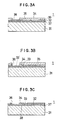
- Figs. 3(A) to 3(C) illustrate the manufacture of a semiconductor device including a carbon film pattern by a process in accordance with the present invention.
- the device was formed within and on a silicon semiconductor substrate 31.
- a silicon oxide film 37 and a superconducting ceramic film 32 were formed and patterned respectively, followed by a coating of a 0.5 micron blocking film 33 which prevents the underlying film 32 from being exposed to etching.
- the blocking film 33 was made of SiO2.
- a carbon film 34 was deposited on the structure to a thickness of from 0.1 to 2 microns, e.g. 0.5 micron.
- a photoresist pattern was formed on the carbon film 34 with an opening 36.
- the opening 36 is designated as a bonding pad for making contact with an IC chip.
- the thickness of the photoresist pattern was selected so that the underlying surface would not be exposed even if the photoresist was partially removed by the following etching.
- oxygen gas was introduced into the reaction chamber and high frequency power was inputted at 300W to perform etching of the carbon film 34.
- the photoresist 35 and a portion of the blocking film 34 at the opening was removed by etching using NF3 or SF6.
- the conductive film 32 may be formed of Al, Ag or Si.
- the blocking film 33 may be formed of a phosphosilicate glass.
- the thickness of the blocking film may be 0.1 to 2 microns in general.
- a silicon oxide pattern may be formed by providing a coating of silicon oxide film and etching the same with a photoresist. Silicon oxide is not subject to etching by oxygen.
- Examples of the latter general formulae are Bi4Sr y Ca3Cu4O x , Bi4Sr y Ca3Cu4O x , Bi4SR y Ca3Cu4O x , Bi4Sr y Ca3Cu4O x , Bi4Sr y Ca3Cu4O x , Bi4SR y Ca3Cu4O x , (y is around 1.5).
- Groups Ia, IIa, VIII, Ib, IIb and 0 are the same in the Japanese and European Periodic Tables
- Groups IIIa, IVa, Va, VIa and VIIb of the Japanese Periodic Table correspond respectively to Groups IIIb, IVb, Vb, VIb and VIIb of the European Periodic Table
- Groups IIIb, IVb, Vb, VIb and VIIb of the Japanese Periodic Table correspond respectively to Groups IIIa, IVa, Va, VIa and VIIa of the European Periodic Table.
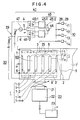
- FIG. 4 Another embodiment of the invention will now be described. Similar elements to those described with reference to Fig. 1 are given the same reference numerals in Fig. 4 and no redundant explanation for such elements will be given.
- the power source 41 is a particular feature of the Fig. 4 embodiment.
- the source 41 comprises a pair of high frequency sources 45-1 and 45-2 which are coupled by a phase shifter 46.
- the phase difference between the outputs of the sources 45-1 and 45-2 is controlled by means of the phase shifter 46.
- the outputs of the sources 45-1 and 45-2 are coupled to a pair of matching transformers 46-1 and 46-2 which, in turn, are coupled in series with each other at respective terminals of their secondary coils, the other terminals of the secondary coils of the transformers 46-1 and 46-2 being connected to the pair of mesh electrodes 3, 3′ in the same manner as in the first embodiment.
- An AC power source 47 and a bias arrangement 29 are connected between the pair of mesh electrodes 3 and 3′ in the same manner as in the first embodiment.
- the relative phases of the electric voltages applied to the electrodes 3 and 3′ are controlled by means of the phase shifter 46 in order to ensure a uniform distribution of plasma throughout the reaction space.
- the potentials at the pair of electrodes 3 and 3′ are basically maintained in phase or in phase opposition, but phase difference may be adjusted to any other suitable angle to adapt to the arrangement of the electrodes within the enclosure 2.
- FIG. 4 An exemplary deposition method by use of the apparatus of Fig. 4 will be explained.
- a number of printing drums 1 for electrostatic copying machines are mounted on substrate holders which are integrally formed as parts of the enclosure 2.
- the surfaces of the printing drums have previously been coated with an organic photoconductive film.
- An exemplary mounting arrangement of the drums in a 50 cm high square enclosure of 75 cm side wall is illustrated in Fig. 5(A) which shows 16 drums to be coated mounted spaced apart from the walls of the enclosure while dummy drums 1-0 are provided along the inner surface of the enclosure in order to make the electric field induced in the plasma generating space 60 more uniform.
- Fig. 5(B) shows an alternative arrangement of drums mounted in a hexagonal enclosure.
- NF3 and C2H2 for example are introduced into the reaction chamber as a reactive gas.
- the ratio of NF3/C2H2 may be from 1/4 to 4/1, e.g. 1/1.
- a plasma is generated and a carbon film is deposited on the drums.
- the carbon film is formed while being subjected to a sputtering action which is mainly induced by the power source 47.
- the carbon film becomes a diamond like carbon film containing nitrogen at 0.3 to 10 atom% and fluorine at 0.3 to 3 atom%.
- the transparency and the resistivity of the diamond like carbon can be controlled by varying the proportions of nitrogen and fluorine. From the viewpoint of the application to printing drums, a suitable resistivity may be found in the range of 1 x 10⁷ to 1 x 10¹⁴ ohm cm, preferably 1 x 10⁹ to 1 x 10¹¹ ohm cm.
- Fig. 6(A) is a cross sectional view showing the form of a printing drum.
- the drum comprises an aluminium cylinder 51 having one end closed and provided with a projection for enabling the drums to be rotatably supported in a copying machine.
- the inner surface of the other end of the drum is screw-threaded at 53.
- a photosensitive dual film 57 consisting of an organic photoconductor film and a carrier transmission film is coated on the aluminium cylinder 51.
- the carbon film 54 is formed so as to cover the dual film 57.
- the thickness of the carbon film may be from 0.1 to 3.0 microns.
- Fig. 6(B) is an enlarged view of part of Fig. 6(A).
- the thickened portion 55 can be formed by locating the end portions near to the mesh electrodes 3 and 3′ and adjusting the plasma pressure to be in a range of from 0.08 to 0.1 Torr.
- the configuration shown in Fig. 6(B) is realised when the plasma pressure is 0.05 Torr.
- the end portions of the carbon film may be dispensed with as shown in Fig. 6(D). This can be realised by adjusting the plasma pressure to be in a range of from 0.01 to 0.04 Torr or by masking the end portions with suitable covers.
- the drums are removed from the chamber, and the inside of the chamber, which may have undesired carbon deposits may be cleaned by introducing an etchant comprising oxygen and effecting plasma etching. Subsequently, H2 plasma etching may be effected to eliminate oxide contaminants attached to the inside of the reaction chamber. Otherwise, the deposition and etching conditions are the same as for the plasma process of the first embodiment.
- FIG. 7 A modification of the apparatus shown in Fig. 4 is illustrated in Fig. 7.
- the same reference numerals are given to the same or similar elements in Fig. 7 as in Fig. 4.
- 56-1 and 56-2 are matching boxes of LCR by means of which impedance matching between the electrodes 3 and 3′ and the high frequency electric power sources 45-1 and 45-2 is established.
- the electric power sources are provided with earth lines 55-1 and 55-2.
- the frequency of one of the electric power sources is equal to or a multiple of that of the other.
- An intermediate voltage supply is connected to the substrate holder 2 and comprises an AC voltage source 57-1, a DC voltage source 57-2, and a three-way switch 51.
- the DC voltage source 57-2 functions to superimpose a DC bias voltage on the AC voltage from the AC voltage source 57-1.
- the frequency of the AC voltage source is from 10Hz to 100KHz.
- the switch 51 three states of bias application can be selected.
- the substrates 1 are rendered electrically floating with the switch at 51-1, are subjected to the AC voltage from the AC source 57-1 biassed by the DC voltage of the source 57-2 with the switch at 51-2, and are earthed with the switch at 51-3.
- the input energy is 0.5 to 50 KW (0.005 to 5 W/cm2), for example 1 KW (0.1 W/cm2).
- phase difference between the voltages at the electrodes 3 and 3′ is adjusted by means of phase shifter 46 in order to spread plasma gas over the whole of the deposition space. If the deposition system is exactly symmetrical with respect to the electrodes 3 and 3′, the phase difference will be set to 0° or 180°. However, depending on any assymetry that might exist, the optimum value may be displaced from 0° or 180°. In accordance with experimental results, the optimum phase difference values were found to be in a range of ⁇ 30° or 180° ⁇ 30°. Plasma gas tended to collect mainly near one of the electrodes 3, 3′ when the phase difference was around 90° or 270° ( ⁇ 30°).
- Carbon films were deposited on printing drums 1 coated with organic photoconductive films by means of the apparatus of Fig. 7.
- the drums were not specially heated and were maintained within a temperature range of room temperature to 150°C.
- a negative bias voltage of -50 to -600 V was established by applying an AC bias voltage from the intermediate voltage supply 57-1.
- Other deposition conditions were the same as for the first embodiment described hereinbefore.
- diamond like carbon films containing fluorine and of 0.1 to 8 microns thickness were formed on the drums at a deposition speed of 1000 ⁇ /min.
- the formation was carried out in two steps. First, ethylene and hydrogen were used in order to deposit carbon thin films of 0.01 to 0.1 micron thickness which has a high adhesitivity to the organic surface of the drums. The resistivity of the films was 1 x 10⁶ to 5 x 10¹³ ohm cm. Next, 0.2 to 2 microns thick carbon films were deposited on the underlying thin carbon films by use of a reactive gas consisting of C2F6 and NH3. The resistivity of the films were 1 x 10⁷ to 5 x 10¹² ohm cm.
- Fig. 8(A) the deposition of silicon nitride films and fluorine containing carbon films will now be explained.
- Glass substrates 11 and 11′ are supported on the substrate holder 2.
- the substrates are, for example, front, side and rear window panes and side mirrors of motor-cars, and similar parts for motor-cycles, other road or rail vehicles or airplanes, or windows for buildings.
- a silicon nitride film 45-1 is formed on the substrate in advance of the carbon coating 45-2 because glass tends to react with fluoride.
- the resistivity of the carbon films was adjusted to be 1 x 10⁶ to 5 x 10¹³ ohm cm by controlling the introduction of fluorine in order to prevent the finished product from gathering dust due to electrostatic effects.
- Fig. 8(B) shows the deposition on a curved surface.
- thermal diffusion of IC chips may be expedited by coating their rear surfaces with the carbon film in advance.
- the substrate to be coated in accordance with the present invention may be made of any material, such as plastics, e.g. PET (polyethyleneterephthalate), PES, PMMA, tefon, epoxy, polyimide or other organic resin.
- PET polyethyleneterephthalate
- PES polyethyleneterephthalate
- PMMA polymethyl methacrylate
- tefon epoxy
- polyimide polyimide
- the substrate can take substantially any shape and can have irregular surfaces.
- the materials that can be deposited on a substrate in accordance with the teachings of the present invention are not limited to carbon, and can include silicon oxide, silicon nitride, and other materials.
- An excellent loudspeaker can be realised by utilising a vibration cone whose inside and outside surfaces have been coated with a very hard carbon film in accordance with the present invention.
- Both side surfaces can be coated at once in a reaction chamber according to the present invention.
Landscapes
- Chemical & Material Sciences (AREA)
- Engineering & Computer Science (AREA)
- Physics & Mathematics (AREA)
- Plasma & Fusion (AREA)
- Analytical Chemistry (AREA)
- Chemical Kinetics & Catalysis (AREA)
- General Chemical & Material Sciences (AREA)
- Materials Engineering (AREA)
- Mechanical Engineering (AREA)
- Metallurgy (AREA)
- Organic Chemistry (AREA)
- Inorganic Chemistry (AREA)
- Chemical Vapour Deposition (AREA)
- Physical Vapour Deposition (AREA)
Applications Claiming Priority (10)
| Application Number | Priority Date | Filing Date | Title |
|---|---|---|---|
| JP25919/88 | 1988-02-05 | ||
| JP2591988A JPH0627341B2 (ja) | 1988-02-05 | 1988-02-05 | 薄膜形成方法 |
| JP25920/88 | 1988-02-05 | ||
| JP63025920A JPH0627342B2 (ja) | 1988-02-05 | 1988-02-05 | 炭素膜形成方法 |
| JP63117792A JP2799414B2 (ja) | 1988-05-13 | 1988-05-13 | プラズマcvd装置および成膜方法 |
| JP117792/88 | 1988-05-13 | ||
| JP212890/88 | 1988-08-26 | ||
| JP21289088A JP2676085B2 (ja) | 1988-08-26 | 1988-08-26 | プラズマ処理装置およびプラズマ処理方法 |
| JP63255489A JPH02101744A (ja) | 1988-10-11 | 1988-10-11 | プラズマ反応方法 |
| JP255489/88 | 1988-10-11 |
Publications (3)
| Publication Number | Publication Date |
|---|---|
| EP0327406A2 true EP0327406A2 (de) | 1989-08-09 |
| EP0327406A3 EP0327406A3 (de) | 1990-11-28 |
| EP0327406B1 EP0327406B1 (de) | 1998-10-14 |
Family
ID=27520783
Family Applications (1)
| Application Number | Title | Priority Date | Filing Date |
|---|---|---|---|
| EP89301126A Expired - Lifetime EP0327406B1 (de) | 1988-02-05 | 1989-02-06 | Plasmabearbeitungsmethode und Vorrichtung zum Aufbringen von Dünnschichten |
Country Status (4)
| Country | Link |
|---|---|
| US (1) | US4971667A (de) |
| EP (1) | EP0327406B1 (de) |
| KR (1) | KR920003431B1 (de) |
| DE (1) | DE68928829T2 (de) |
Cited By (1)
| Publication number | Priority date | Publication date | Assignee | Title |
|---|---|---|---|---|
| EP0359567A3 (de) * | 1988-09-16 | 1991-01-16 | Semiconductor Energy Laboratory Co., Ltd. | Verfahren und Vorrichtung zur Plasmabehandlung |
Families Citing this family (38)
| Publication number | Priority date | Publication date | Assignee | Title |
|---|---|---|---|---|
| EP0283620A1 (de) | 1987-03-25 | 1988-09-28 | Semiconductor Energy Laboratory Co., Ltd. | Supraleitende Keramiken |
| JP2630361B2 (ja) * | 1987-03-27 | 1997-07-16 | 株式会社 半導体エネルギー研究所 | 超電導材料 |
| US5230931A (en) * | 1987-08-10 | 1993-07-27 | Semiconductor Energy Laboratory Co., Ltd. | Plasma-assisted cvd of carbonaceous films by using a bias voltage |
| US5411797A (en) * | 1988-04-18 | 1995-05-02 | Board Of Regents, The University Of Texas System | Nanophase diamond films |
| EP0342681B1 (de) * | 1988-05-19 | 1995-08-09 | Semiconductor Energy Laboratory Co., Ltd. | Verfahren zur Herstellung einer elektrischen Vorrichtung |
| US5163458A (en) * | 1989-08-03 | 1992-11-17 | Optek, Inc. | Method for removing contaminants by maintaining the plasma in abnormal glow state |
| US5242663A (en) * | 1989-09-20 | 1993-09-07 | Sumitomo Electric Industries, Ltd. | Method of and apparatus for synthesizing hard material |
| US5227202A (en) * | 1989-09-22 | 1993-07-13 | Balzers Aktiengesellschaft | Method for chemical coating on opposite surfaces of workpieces |
| US5133986A (en) * | 1990-10-05 | 1992-07-28 | International Business Machines Corporation | Plasma enhanced chemical vapor processing system using hollow cathode effect |
| US5087297A (en) * | 1991-01-17 | 1992-02-11 | Johnson Matthey Inc. | Aluminum target for magnetron sputtering and method of making same |
| US5212118A (en) * | 1991-08-09 | 1993-05-18 | Saxena Arjun N | Method for selective chemical vapor deposition of dielectric, semiconductor and conductive films on semiconductor and metallic substrates |
| WO1993008927A1 (en) * | 1991-11-05 | 1993-05-13 | Research Triangle Institute | Chemical vapor deposition of diamond films using water-based plasma discharges |
| CH689767A5 (de) * | 1992-03-24 | 1999-10-15 | Balzers Hochvakuum | Verfahren zur Werkstueckbehandlung in einer Vakuumatmosphaere und Vakuumbehandlungsanlage. |
| US6835523B1 (en) * | 1993-05-09 | 2004-12-28 | Semiconductor Energy Laboratory Co., Ltd. | Apparatus for fabricating coating and method of fabricating the coating |
| JP3107275B2 (ja) * | 1994-08-22 | 2000-11-06 | 東京エレクトロン株式会社 | 半導体製造装置及び半導体製造装置のクリーニング方法 |
| CA2157257C (en) * | 1994-09-12 | 1999-08-10 | Kazuhiko Endo | Semiconductor device with amorphous carbon layer and method of fabricating the same |
| US5535906A (en) * | 1995-01-30 | 1996-07-16 | Advanced Energy Industries, Inc. | Multi-phase DC plasma processing system |
| DE19546826C1 (de) * | 1995-12-15 | 1997-04-03 | Fraunhofer Ges Forschung | Verfahren und Einrichtung zur Vorbehandlung von Substraten |
| DE19601436A1 (de) * | 1996-01-17 | 1997-07-24 | Siegfried Dr Ing Straemke | Verfahren und Vorrichtung zur Oberflächenbehandlung von Werkstücken |
| US5789040A (en) * | 1997-05-21 | 1998-08-04 | Optical Coating Laboratory, Inc. | Methods and apparatus for simultaneous multi-sided coating of optical thin film designs using dual-frequency plasma-enhanced chemical vapor deposition |
| US5766362A (en) * | 1996-09-30 | 1998-06-16 | Becton Dickinson And Company | Apparatus for depositing barrier film on three-dimensional articles |
| JP3582330B2 (ja) * | 1997-11-14 | 2004-10-27 | 東京エレクトロン株式会社 | 処理装置及びこれを用いた処理システム |
| US20010048095A1 (en) | 1998-07-01 | 2001-12-06 | Steven N. Towle | Method for improving thermal stability of fluorinated amorphous carbon low dielectric constant materials |
| JP4141560B2 (ja) * | 1998-12-28 | 2008-08-27 | 日本メクトロン株式会社 | 回路基板のプラズマ処理装置 |
| RU2170283C2 (ru) * | 1998-12-29 | 2001-07-10 | Сенокосов Евгений Степанович | Способ очистки поверхности металлических изделий |
| AU2905901A (en) * | 1999-11-30 | 2001-06-12 | Regents Of The University Of California, The | Method for producing fluorinated diamond-like carbon films |
| JP3989205B2 (ja) * | 2000-08-31 | 2007-10-10 | 松下電器産業株式会社 | Cvd膜の形成方法 |
| US6673302B2 (en) * | 2001-01-24 | 2004-01-06 | Scimed Life Systems, Inc. | Wet processing method for catheter balloons |
| JP2002280354A (ja) * | 2001-03-19 | 2002-09-27 | Osaka Prefecture | 炭素薄膜のエッチング方法及びエッチング装置 |
| US7396735B2 (en) * | 2002-12-09 | 2008-07-08 | Kabushiki Kaisha Toyota Chuo Kenkyusyo | Semiconductor element heat dissipating member, semiconductor device using same, and method for manufacturing same |
| JP4892209B2 (ja) * | 2005-08-22 | 2012-03-07 | 日立化成デュポンマイクロシステムズ株式会社 | 半導体装置の製造方法 |
| JP4691417B2 (ja) * | 2005-08-22 | 2011-06-01 | 日立化成デュポンマイクロシステムズ株式会社 | 回路接続構造体及びその製造方法及び回路接続構造体用の半導体基板 |
| JP5058909B2 (ja) * | 2007-08-17 | 2012-10-24 | 株式会社半導体エネルギー研究所 | プラズマcvd装置及び薄膜トランジスタの作製方法 |
| US8101444B2 (en) * | 2007-08-17 | 2012-01-24 | Semiconductor Energy Laboratory Co., Ltd. | Method for manufacturing semiconductor device |
| US8247315B2 (en) * | 2008-03-17 | 2012-08-21 | Semiconductor Energy Laboratory Co., Ltd. | Plasma processing apparatus and method for manufacturing semiconductor device |
| DE102009052436A1 (de) * | 2009-11-10 | 2011-05-12 | Elena Nikitina | Einrichtung für die Lichtbogenbehandlung der Oberfläche von Metallerzeugnissen |
| KR101472794B1 (ko) * | 2013-04-11 | 2014-12-15 | 한국기계연구원 | 플라즈마 점화 제어 방법 |
| EP3393215A1 (de) | 2017-04-20 | 2018-10-24 | Andrey Senokosov | Lichtbogenplasmatron-oberflächenbehandlung |
Family Cites Families (9)
| Publication number | Priority date | Publication date | Assignee | Title |
|---|---|---|---|---|
| US4582720A (en) * | 1982-09-20 | 1986-04-15 | Semiconductor Energy Laboratory Co., Ltd. | Method and apparatus for forming non-single-crystal layer |
| US4464223A (en) * | 1983-10-03 | 1984-08-07 | Tegal Corp. | Plasma reactor apparatus and method |
| US4581100A (en) * | 1984-10-29 | 1986-04-08 | International Business Machines Corporation | Mixed excitation plasma etching system |
| US4572759A (en) * | 1984-12-26 | 1986-02-25 | Benzing Technology, Inc. | Troide plasma reactor with magnetic enhancement |
| US4618477A (en) * | 1985-01-17 | 1986-10-21 | International Business Machines Corporation | Uniform plasma for drill smear removal reactor |
| US4585516A (en) * | 1985-03-04 | 1986-04-29 | Tegal Corporation | Variable duty cycle, multiple frequency, plasma reactor |
| JP2616760B2 (ja) * | 1985-04-08 | 1997-06-04 | 株式会社 半導体エネルギー研究所 | プラズマ気相反応装置 |
| KR910003169B1 (ko) * | 1985-11-12 | 1991-05-20 | 가부시끼가이샤 한도다이 에네르기 겐뀨소 | 반도체 장치 제조 방법 및 장치 |
| GB8629634D0 (en) * | 1986-12-11 | 1987-01-21 | Dobson C D | Reactive ion & sputter etching |
-
1989
- 1989-02-03 KR KR1019890001263A patent/KR920003431B1/ko not_active Expired
- 1989-02-03 US US07/303,240 patent/US4971667A/en not_active Expired - Lifetime
- 1989-02-06 EP EP89301126A patent/EP0327406B1/de not_active Expired - Lifetime
- 1989-02-06 DE DE68928829T patent/DE68928829T2/de not_active Expired - Fee Related
Cited By (1)
| Publication number | Priority date | Publication date | Assignee | Title |
|---|---|---|---|---|
| EP0359567A3 (de) * | 1988-09-16 | 1991-01-16 | Semiconductor Energy Laboratory Co., Ltd. | Verfahren und Vorrichtung zur Plasmabehandlung |
Also Published As
| Publication number | Publication date |
|---|---|
| KR890013966A (ko) | 1989-09-26 |
| DE68928829D1 (de) | 1998-11-19 |
| DE68928829T2 (de) | 1999-06-17 |
| EP0327406B1 (de) | 1998-10-14 |
| US4971667A (en) | 1990-11-20 |
| EP0327406A3 (de) | 1990-11-28 |
| KR920003431B1 (ko) | 1992-05-01 |
Similar Documents
| Publication | Publication Date | Title |
|---|---|---|
| EP0327406A2 (de) | Plasmabearbeitungsmethode und Vorrichtung zum Aufbringen von Dünnschichten | |
| US5283087A (en) | Plasma processing method and apparatus | |
| US5030476A (en) | Process and apparatus for the formation of a functional deposited film on a cylindrical substrate by means of microwave plasma chemical vapor deposition | |
| US5230931A (en) | Plasma-assisted cvd of carbonaceous films by using a bias voltage | |
| US5079031A (en) | Apparatus and method for forming thin films | |
| US6265070B1 (en) | Electrostatic-erasing abrasion-proof coating and method for forming the same | |
| EP0717127B1 (de) | Verfahren und Vorrichtung zur Plasmabehandlung | |
| US20030143410A1 (en) | Method for reduction of contaminants in amorphous-silicon film | |
| CN1035855A (zh) | 淀积主要由碳组成的薄膜的方法 | |
| JP2000514246A (ja) | 低圧プラズマ反応装置内における透明電極のドライエッチング法 | |
| US5145711A (en) | Cyclotron resonance chemical vapor deposition method of forming a halogen-containing diamond on a substrate | |
| US5120625A (en) | Carbon material containing a halogen and deposition method for same | |
| US5256483A (en) | Plasma processing method and apparatus | |
| US4987004A (en) | Plasma processing method and apparatus | |
| US5007374A (en) | Apparatus for forming thin films in quantity | |
| US6224952B1 (en) | Electrostatic-erasing abrasion-proof coating and method for forming the same | |
| CN1021100C (zh) | 等离子体处理方法和装置 | |
| JPH0776781A (ja) | プラズマ気相成長装置 | |
| JP2564627B2 (ja) | 炭素膜で覆われた部材およびその作製方法 | |
| JP2700177B2 (ja) | 薄膜形成方法と装置 | |
| JP2775263B2 (ja) | 炭素膜で覆われた部材 | |
| US5098812A (en) | Photosensitive device and manufacturing method for the same | |
| JP3256212B2 (ja) | ダイヤモンド状炭素膜の作製方法 | |
| JP3254202B2 (ja) | 炭素膜または炭素を主成分とする膜が設けられた部材 | |
| JP2000226666A (ja) | ダイヤモンド状炭素膜の作製方法 |
Legal Events
| Date | Code | Title | Description |
|---|---|---|---|
| PUAI | Public reference made under article 153(3) epc to a published international application that has entered the european phase |
Free format text: ORIGINAL CODE: 0009012 |
|
| AK | Designated contracting states |
Kind code of ref document: A2 Designated state(s): DE FR GB |
|
| PUAL | Search report despatched |
Free format text: ORIGINAL CODE: 0009013 |
|
| AK | Designated contracting states |
Kind code of ref document: A3 Designated state(s): DE FR GB |
|
| 17P | Request for examination filed |
Effective date: 19901214 |
|
| 17Q | First examination report despatched |
Effective date: 19930422 |
|
| GRAG | Despatch of communication of intention to grant |
Free format text: ORIGINAL CODE: EPIDOS AGRA |
|
| GRAG | Despatch of communication of intention to grant |
Free format text: ORIGINAL CODE: EPIDOS AGRA |
|
| GRAH | Despatch of communication of intention to grant a patent |
Free format text: ORIGINAL CODE: EPIDOS IGRA |
|
| GRAH | Despatch of communication of intention to grant a patent |
Free format text: ORIGINAL CODE: EPIDOS IGRA |
|
| GRAA | (expected) grant |
Free format text: ORIGINAL CODE: 0009210 |
|
| AK | Designated contracting states |
Kind code of ref document: B1 Designated state(s): DE FR GB |
|
| REF | Corresponds to: |
Ref document number: 68928829 Country of ref document: DE Date of ref document: 19981119 |
|
| ET | Fr: translation filed | ||
| PLBE | No opposition filed within time limit |
Free format text: ORIGINAL CODE: 0009261 |
|
| STAA | Information on the status of an ep patent application or granted ep patent |
Free format text: STATUS: NO OPPOSITION FILED WITHIN TIME LIMIT |
|
| 26N | No opposition filed | ||
| REG | Reference to a national code |
Ref country code: GB Ref legal event code: IF02 |
|
| PGFP | Annual fee paid to national office [announced via postgrant information from national office to epo] |
Ref country code: GB Payment date: 20070131 Year of fee payment: 19 |
|
| PGFP | Annual fee paid to national office [announced via postgrant information from national office to epo] |
Ref country code: DE Payment date: 20070201 Year of fee payment: 19 |
|
| PGFP | Annual fee paid to national office [announced via postgrant information from national office to epo] |
Ref country code: FR Payment date: 20070208 Year of fee payment: 19 |
|
| GBPC | Gb: european patent ceased through non-payment of renewal fee |
Effective date: 20080206 |
|
| REG | Reference to a national code |
Ref country code: FR Ref legal event code: ST Effective date: 20081031 |
|
| PG25 | Lapsed in a contracting state [announced via postgrant information from national office to epo] |
Ref country code: DE Free format text: LAPSE BECAUSE OF NON-PAYMENT OF DUE FEES Effective date: 20080902 |
|
| PG25 | Lapsed in a contracting state [announced via postgrant information from national office to epo] |
Ref country code: FR Free format text: LAPSE BECAUSE OF NON-PAYMENT OF DUE FEES Effective date: 20080229 |
|
| PG25 | Lapsed in a contracting state [announced via postgrant information from national office to epo] |
Ref country code: GB Free format text: LAPSE BECAUSE OF NON-PAYMENT OF DUE FEES Effective date: 20080206 |