EP0328077A2 - Arrangement pour la protection des dispositifs électroniques contre de l'électricité statique - Google Patents
Arrangement pour la protection des dispositifs électroniques contre de l'électricité statique Download PDFInfo
- Publication number
- EP0328077A2 EP0328077A2 EP89102165A EP89102165A EP0328077A2 EP 0328077 A2 EP0328077 A2 EP 0328077A2 EP 89102165 A EP89102165 A EP 89102165A EP 89102165 A EP89102165 A EP 89102165A EP 0328077 A2 EP0328077 A2 EP 0328077A2
- Authority
- EP
- European Patent Office
- Prior art keywords
- terminals
- connector
- memory card
- shutter
- contact
- Prior art date
- Legal status (The legal status is an assumption and is not a legal conclusion. Google has not performed a legal analysis and makes no representation as to the accuracy of the status listed.)
- Granted
Links
Images

Classifications
-
- H—ELECTRICITY
- H01—ELECTRIC ELEMENTS
- H01R—ELECTRICALLY-CONDUCTIVE CONNECTIONS; STRUCTURAL ASSOCIATIONS OF A PLURALITY OF MUTUALLY-INSULATED ELECTRICAL CONNECTING ELEMENTS; COUPLING DEVICES; CURRENT COLLECTORS
- H01R31/00—Coupling parts supported only by co-operation with counterpart
- H01R31/08—Short-circuiting members for bridging contacts in a counterpart
-
- H—ELECTRICITY
- H05—ELECTRIC TECHNIQUES NOT OTHERWISE PROVIDED FOR
- H05K—PRINTED CIRCUITS; CASINGS OR CONSTRUCTIONAL DETAILS OF ELECTRIC APPARATUS; MANUFACTURE OF ASSEMBLAGES OF ELECTRICAL COMPONENTS
- H05K5/00—Casings, cabinets or drawers for electric apparatus
- H05K5/02—Details
- H05K5/0256—Details of interchangeable modules or receptacles therefor, e.g. cartridge mechanisms
- H05K5/0286—Receptacles therefor, e.g. card slots, module sockets, card groundings
-
- G—PHYSICS
- G06—COMPUTING OR CALCULATING; COUNTING
- G06K—GRAPHICAL DATA READING; PRESENTATION OF DATA; RECORD CARRIERS; HANDLING RECORD CARRIERS
- G06K19/00—Record carriers for use with machines and with at least a part designed to carry digital markings
- G06K19/06—Record carriers for use with machines and with at least a part designed to carry digital markings characterised by the kind of the digital marking, e.g. shape, nature, code
- G06K19/067—Record carriers with conductive marks, printed circuits or semiconductor circuit elements, e.g. credit or identity cards also with resonating or responding marks without active components
- G06K19/07—Record carriers with conductive marks, printed circuits or semiconductor circuit elements, e.g. credit or identity cards also with resonating or responding marks without active components with integrated circuit chips
- G06K19/077—Constructional details, e.g. mounting of circuits in the carrier
- G06K19/0772—Physical layout of the record carrier
- G06K19/07735—Physical layout of the record carrier the record carrier comprising means for protecting against electrostatic discharge
-
- G—PHYSICS
- G06—COMPUTING OR CALCULATING; COUNTING
- G06K—GRAPHICAL DATA READING; PRESENTATION OF DATA; RECORD CARRIERS; HANDLING RECORD CARRIERS
- G06K7/00—Methods or arrangements for sensing record carriers, e.g. for reading patterns
- G06K7/0013—Methods or arrangements for sensing record carriers, e.g. for reading patterns by galvanic contacts, e.g. card connectors for ISO-7816 compliant smart cards or memory cards, e.g. SD card readers
- G06K7/0047—Methods or arrangements for sensing record carriers, e.g. for reading patterns by galvanic contacts, e.g. card connectors for ISO-7816 compliant smart cards or memory cards, e.g. SD card readers for reading/sensing record carriers having edge contacts
-
- G—PHYSICS
- G06—COMPUTING OR CALCULATING; COUNTING
- G06K—GRAPHICAL DATA READING; PRESENTATION OF DATA; RECORD CARRIERS; HANDLING RECORD CARRIERS
- G06K7/00—Methods or arrangements for sensing record carriers, e.g. for reading patterns
- G06K7/0013—Methods or arrangements for sensing record carriers, e.g. for reading patterns by galvanic contacts, e.g. card connectors for ISO-7816 compliant smart cards or memory cards, e.g. SD card readers
- G06K7/0056—Methods or arrangements for sensing record carriers, e.g. for reading patterns by galvanic contacts, e.g. card connectors for ISO-7816 compliant smart cards or memory cards, e.g. SD card readers housing of the card connector
- G06K7/0082—Methods or arrangements for sensing record carriers, e.g. for reading patterns by galvanic contacts, e.g. card connectors for ISO-7816 compliant smart cards or memory cards, e.g. SD card readers housing of the card connector comprising an arrangement for protection against electrostatic discharge, e.g. by grounding part of the conductive housing
-
- H—ELECTRICITY
- H01—ELECTRIC ELEMENTS
- H01R—ELECTRICALLY-CONDUCTIVE CONNECTIONS; STRUCTURAL ASSOCIATIONS OF A PLURALITY OF MUTUALLY-INSULATED ELECTRICAL CONNECTING ELEMENTS; COUPLING DEVICES; CURRENT COLLECTORS
- H01R13/00—Details of coupling devices of the kinds covered by groups H01R12/70 or H01R24/00 - H01R33/00
- H01R13/648—Protective earth or shield arrangements on coupling devices, e.g. anti-static shielding
- H01R13/6485—Electrostatic discharge protection
-
- H—ELECTRICITY
- H05—ELECTRIC TECHNIQUES NOT OTHERWISE PROVIDED FOR
- H05K—PRINTED CIRCUITS; CASINGS OR CONSTRUCTIONAL DETAILS OF ELECTRIC APPARATUS; MANUFACTURE OF ASSEMBLAGES OF ELECTRICAL COMPONENTS
- H05K9/00—Screening of apparatus or components against electric or magnetic fields
- H05K9/0067—Devices for protecting against damage from electrostatic discharge
-
- H—ELECTRICITY
- H01—ELECTRIC ELEMENTS
- H01R—ELECTRICALLY-CONDUCTIVE CONNECTIONS; STRUCTURAL ASSOCIATIONS OF A PLURALITY OF MUTUALLY-INSULATED ELECTRICAL CONNECTING ELEMENTS; COUPLING DEVICES; CURRENT COLLECTORS
- H01R13/00—Details of coupling devices of the kinds covered by groups H01R12/70 or H01R24/00 - H01R33/00
- H01R13/44—Means for preventing access to live contacts
- H01R13/447—Shutter or cover plate
- H01R13/453—Shutter or cover plate opened by engagement of counterpart
Definitions
- the present invention relates to an arrangement for removing electric charges which may be present or generated when an electronic apparatus is connected to a connector.
- JP-A-62-77996 describes an integrated circuit card provided with a slidable shutter to protect terminals of the integrated circuit card and to expose them only when the terminals are to be connected to the terminals of a connector. Pins are provided for opening/closing the shutter. This document does, however, not describe any construction for removing electric charges which may be generated at the time when the terminals of the integrated circuit card are connected to the terminals of the connector.
- a contacting member of the electronic apparatus is electrically connected to a contacting member of the connector before the terminals of the electronic apparatus come into contact with the terminals of the connector.
- the contacting member of the connector is electrically connected to the casing of the electronic device of which the connector is a part. Due to this construction, any charges generated in the electronic apparatus, for instance a memory card, are discharged to the ground of the electronic device, so that the electronic circuitry connected to the terminals can be protected from being affected by such charge.
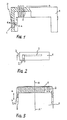
- Fig. 1 shows a plan view, partially in section, of a connector according to one embodiment of the present invention.
- Fig. 2 is a side view from the left side of the connector.
- Fig. 3 is a bottom plan view, partially in section, of a memory card which is used as one example of an electronic apparatus to be connected to the connector of Figs. 1 and 2. It should be understood that the invention is of course not only applicable for memory cards but for a variety of electronic apparatus.
- the connector shown in Figs. 1 and 2 has a U-shaped housing 4 with a front part and two side parts.
- terminals 3 are provided which will be connected to terminals 9 of the memory card when the latter is introduced into the connector as will be described later.
- Terminals 3 extend into the inside of the housing 4.
- the connector will normally be part of an electric device and have its terminals 3 connected to the circuitry of this device.
- Each contacting member comprises a pin 2 for securing the contacting member to the housing 4.
- a pawl 1b Integrally formed with the pin is a pawl 1b provided with a projection 1a which projects into the interior of the housing 4.
- the contacting members 1 are made of electrically conductive metal and are resiliently urged towards the inside of the housing 4. Via the pins 2 or by other means the contact members 1 are electrically connected to a case of the device and, thus, normally to ground.
- projections 4a of which only the one on the left side is shown in Fig. 1.
- the contacting members 1 of the connector serve to discharge any electric charge from the memory card as it is being inserted into the connector and before its terminals 9 come into contact the terminals 3 of the connector as will be explained in detail later.
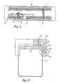
- Fig. 3 is a bottom plan view of the memory card, a diagrammatic sectional view of which along line A-A′ being shown in Fig. 4.
- the memory card includes a circuit substrate 8 on which the terminals 9 and integrated circuits (not shown) are provided.
- the circuit substrate 8 is sandwiched with metal panels 6 for protecting the integrated circuits on the circuit substrate 8 against external forces, static electricity, noise and so on.
- Insulating layers 10 are provided on the confronting inner sides of the metal panels 6. Both metal panels 6 are electrically connected with each other as by a coil spring 7.
- a shutter 5 is provided to protect terminals 9 of the memory card against dust, external forces and static electricity as long as the memory card is not inserted into the connector.
- the shutter 5 is slidably guided in the directions of arrows a and b between a protecting position shown in Fig. 4 and a retracted position shown in Fig. 6 where the terminals 9 are exposed.
- the shutter 5 which is made of an electrically conductive metal is slidable on the lower one of the metal panels 6 and, thus, is electrically connected to the metal panels.
- the shutter 5 In its protecting position, the shutter 5 preferably also contacts terminals 9 of the circuit substrate 8 so that in this position of the shutter 5, the circuits on the circuit substrate 8 and the metal pla tes 6 of the memory card are forced to have the same electric potential.
- the shutter 5 is biased by a spring (not shown) into its protecting position of Fig. 4.
- the shutter 5 has on each side a projection 5a to be contacted by projections 4a and projections 1a of the connector when the memory card is inserted into the connector.
- the projections 5a thus serve as contacting members of the memory card.
- Fig. 5 shows the memory card partly, not fully inserted into the connector.
- Fig. 6 is similar to Fig. 5 showing, however, the condition when the memory card is completely inserted into the connector and has its terminals 9 connected with the terminals 3 of the connector.
- the projections 1a of the connecting members 1 of the connector will come into contact with the projections 5a of the shutter 5 of the memory card.
- the shutter 5, the metal plates 6 and preferably the terminals 9 of the memory card are electrically connected via the connecting members 1 of the connector to ground so that any charges that may exist on the memory card are discharged to ground.
- the projections 5a of the shutter 5 will abut against the projections 4a of the connector, preventing the shutter 5 from being moved further towards the front part of the connector. A further movement of the memory card thus results in a relative movement between the shutter 5 and the rest of the memory card, transferring the shutter 5 into its retracted position.
- shutter 5 of the memory card is electrically connected to the ground of the apparatus via the connecting members 1 and its pins 2, the memory card will be unaffected by static electricity.
- the shutter 5 When the memory card is removed from the connector, the shutter 5 while still being electrically connected to the contacting members 1 will be closed again and the contact between the projections 5a of the shutter 5 and the projections 1a of the connecting members 1 will be broken only after the shutter has reached its protecting position and the terminals 9 of the memory card have been disconnected from the terminals 3 of the connector.
Landscapes
- Engineering & Computer Science (AREA)
- Microelectronics & Electronic Packaging (AREA)
- Physics & Mathematics (AREA)
- General Physics & Mathematics (AREA)
- Theoretical Computer Science (AREA)
- Artificial Intelligence (AREA)
- Computer Vision & Pattern Recognition (AREA)
- Computer Hardware Design (AREA)
- Details Of Connecting Devices For Male And Female Coupling (AREA)
- Coupling Device And Connection With Printed Circuit (AREA)
- Credit Cards Or The Like (AREA)
- Elimination Of Static Electricity (AREA)
Applications Claiming Priority (2)
| Application Number | Priority Date | Filing Date | Title |
|---|---|---|---|
| JP17295/88U | 1988-02-12 | ||
| JP1729588 | 1988-02-12 |
Publications (3)
| Publication Number | Publication Date |
|---|---|
| EP0328077A2 true EP0328077A2 (fr) | 1989-08-16 |
| EP0328077A3 EP0328077A3 (en) | 1990-07-04 |
| EP0328077B1 EP0328077B1 (fr) | 1994-06-08 |
Family
ID=11940006
Family Applications (1)
| Application Number | Title | Priority Date | Filing Date |
|---|---|---|---|
| EP89102165A Expired - Lifetime EP0328077B1 (fr) | 1988-02-12 | 1989-02-08 | Arrangement pour la protection des dispositifs électroniques contre de l'électricité statique |
Country Status (4)
| Country | Link |
|---|---|
| US (1) | US4955817A (fr) |
| EP (1) | EP0328077B1 (fr) |
| KR (1) | KR930009394B1 (fr) |
| DE (1) | DE68915799T2 (fr) |
Cited By (5)
| Publication number | Priority date | Publication date | Assignee | Title |
|---|---|---|---|---|
| EP0532166A1 (fr) * | 1991-09-11 | 1993-03-17 | ITT INDUSTRIES, INC. (a Delaware corporation) | Appareil de mise à la terre pour carte de mémoire |
| WO1993017471A1 (fr) * | 1992-02-24 | 1993-09-02 | Itt Industries, Inc. | Ressort de mise a la terre d'une carte memoire |
| EP0678830A1 (fr) * | 1994-04-12 | 1995-10-25 | Molex Incorporated | Système de mise à la terre pour des cartes de circuit intégré |
| EP0936705A3 (fr) * | 1998-02-10 | 2001-02-14 | The Great American Gumball Corporation | Adapteur pour dispositif périphérique d'un ordinateur personnel |
| EP1276176A3 (fr) * | 2001-07-13 | 2003-12-10 | Hosiden Corporation | Connecteur à obturateur |
Families Citing this family (28)
| Publication number | Priority date | Publication date | Assignee | Title |
|---|---|---|---|---|
| US5305180A (en) * | 1991-06-06 | 1994-04-19 | Grid Systems Corporation | Disk drive ejector mechanism with latch and ejector and standby switch |
| US5544007A (en) * | 1991-07-19 | 1996-08-06 | Kabushiiki Kaisha Toshiba | Card-shaped electronic device used with an electronic apparatus and having shield plate with conductive portion on a lateral side |
| CA2071381C (fr) * | 1991-07-19 | 1998-12-15 | Youji Satou | Appareil electronique, element electronique du type carte utilise avec cet appareil et systeme electronique a dispositif d'expansion de fonctions |
| US5404271A (en) * | 1991-07-30 | 1995-04-04 | Kabushiki Kaisha Toshiba | Electronic apparatus having a card storing section formed within a body between a support frame and an upper case of the body and having functional elements mounted between the support frame and a lower case of the body |
| US5504648A (en) * | 1991-09-06 | 1996-04-02 | Kabushiki Kaisha Toshiba | Electronic apparatus and electronic system with expanding apparatus having interlock, ejector, grounding, and lock mechanisms, for expanding function of electronic apparatus |
| EP0682322B1 (fr) * | 1991-09-09 | 2001-09-26 | Itt Manufacturing Enterprises, Inc. | Carte à puce |
| US5207586A (en) * | 1991-10-24 | 1993-05-04 | Intel Corporation | Integral connector system for credit card size I/O card external connector |
| DE4238202C2 (de) * | 1991-11-11 | 1994-10-20 | Kansei Kk | Elektrischer Steckverbinder |
| US5333100A (en) * | 1992-06-29 | 1994-07-26 | Itt Corporation | Data card perimeter shield |
| JPH0654272U (ja) * | 1992-12-29 | 1994-07-22 | ミツミ電機株式会社 | 電気コネクタ |
| US5470241A (en) * | 1993-12-21 | 1995-11-28 | The Whitaker Corporation | Retention mechanism for memory cards |
| US5726867A (en) * | 1994-01-21 | 1998-03-10 | The Whitaker Corporation | Card holder for computers and related equipment |
| US5511986A (en) * | 1994-02-23 | 1996-04-30 | Molex Incorporated | IC pack connector with detect switch |
| US5502620A (en) * | 1994-03-11 | 1996-03-26 | Molex Incorporated | Grounded IC card |
| USRE40150E1 (en) | 1994-04-25 | 2008-03-11 | Matsushita Electric Industrial Co., Ltd. | Fiber optic module |
| US5526235A (en) * | 1994-06-23 | 1996-06-11 | Garmin Communication And Navigation | Electronic storage device and receptacle |
| US5606704A (en) * | 1994-10-26 | 1997-02-25 | Intel Corporation | Active power down for PC card I/O applications |
| US5653596A (en) * | 1995-06-02 | 1997-08-05 | Molex Incorporated | Grounding system for PC cards |
| US5920460A (en) * | 1997-01-11 | 1999-07-06 | Methode Electronics, Inc. | PC card receptacle with integral ground clips |
| US6282097B1 (en) | 1998-10-28 | 2001-08-28 | Garmin Corporation | Data card having a retractable handle |
| US6250553B1 (en) | 1998-12-30 | 2001-06-26 | Garmin Corporation | Data card having a retractable handle |
| SE515495C2 (sv) * | 1999-12-30 | 2001-08-13 | Ericsson Telefon Ab L M | ESD skyddsanordning för en minneskorthållare |
| JP2003257555A (ja) * | 2002-02-26 | 2003-09-12 | Molex Inc | 電気コネクタ |
| US6905350B1 (en) | 2002-04-05 | 2005-06-14 | Maxtor Corporation | Two-step electrical connector and method using high resistance path for electrostatic discharge |
| JP2006178868A (ja) * | 2004-12-24 | 2006-07-06 | Fujitsu Ltd | 電子装置および筐体 |
| US7908080B2 (en) | 2004-12-31 | 2011-03-15 | Google Inc. | Transportation routing |
| DE202008002149U1 (de) * | 2008-02-16 | 2008-04-30 | Harting Electronics Gmbh & Co. Kg | Leiterkarten-Steckverbinder mit Masseanschluss |
| CN104427732B (zh) * | 2013-08-28 | 2017-12-26 | 中兴通讯股份有限公司 | 一种终端及其收集静电、充电的方法 |
Family Cites Families (9)
| Publication number | Priority date | Publication date | Assignee | Title |
|---|---|---|---|---|
| GB1481700A (en) * | 1974-06-06 | 1977-08-03 | Quantel Ltd | Interconnection of circuit boards |
| US4510553A (en) * | 1983-01-24 | 1985-04-09 | Burroughs Corporation | Electromechanical assembly for aligning, discharging, and sequentially engaging conductors of a P.C. board with a backplane |
| JPS60100829U (ja) * | 1983-12-14 | 1985-07-09 | 第一電子工業株式会社 | メモリカ−ド用コネクタ |
| JPS60179982A (ja) * | 1984-02-28 | 1985-09-13 | Canon Inc | 外部記憶用パツク |
| JPS61206299A (ja) * | 1985-03-09 | 1986-09-12 | 株式会社東芝 | 印刷配線板 |
| JPS6277996A (ja) * | 1985-09-30 | 1987-04-10 | 三菱電機株式会社 | Icカ−ド |
| US4780791A (en) * | 1986-04-08 | 1988-10-25 | Fujisoku Electric Co., Ltd. | Card-shaped memory having an IC module |
| US4780793A (en) * | 1986-06-03 | 1988-10-25 | Daiichi Denshi Kogyo Kabushiki Kaisha | IC card and connector therefor |
| JPS63242691A (ja) * | 1987-03-31 | 1988-10-07 | 三菱電機株式会社 | 半導体装置カ−ド |
-
1989
- 1989-02-03 KR KR1019890001270A patent/KR930009394B1/ko not_active Expired - Fee Related
- 1989-02-08 DE DE68915799T patent/DE68915799T2/de not_active Expired - Fee Related
- 1989-02-08 EP EP89102165A patent/EP0328077B1/fr not_active Expired - Lifetime
- 1989-02-10 US US07/308,870 patent/US4955817A/en not_active Expired - Lifetime
Cited By (6)
| Publication number | Priority date | Publication date | Assignee | Title |
|---|---|---|---|---|
| EP0532166A1 (fr) * | 1991-09-11 | 1993-03-17 | ITT INDUSTRIES, INC. (a Delaware corporation) | Appareil de mise à la terre pour carte de mémoire |
| WO1993017471A1 (fr) * | 1992-02-24 | 1993-09-02 | Itt Industries, Inc. | Ressort de mise a la terre d'une carte memoire |
| EP0678830A1 (fr) * | 1994-04-12 | 1995-10-25 | Molex Incorporated | Système de mise à la terre pour des cartes de circuit intégré |
| EP0936705A3 (fr) * | 1998-02-10 | 2001-02-14 | The Great American Gumball Corporation | Adapteur pour dispositif périphérique d'un ordinateur personnel |
| US6413108B2 (en) | 1998-02-10 | 2002-07-02 | Itt Manufacturing Enterprises, Inc. | Personal computer peripheral device adapter |
| EP1276176A3 (fr) * | 2001-07-13 | 2003-12-10 | Hosiden Corporation | Connecteur à obturateur |
Also Published As
| Publication number | Publication date |
|---|---|
| EP0328077B1 (fr) | 1994-06-08 |
| KR890013763A (ko) | 1989-09-25 |
| EP0328077A3 (en) | 1990-07-04 |
| DE68915799T2 (de) | 1994-10-20 |
| DE68915799D1 (de) | 1994-07-14 |
| US4955817A (en) | 1990-09-11 |
| KR930009394B1 (ko) | 1993-10-02 |
Similar Documents
| Publication | Publication Date | Title |
|---|---|---|
| EP0328077A2 (fr) | Arrangement pour la protection des dispositifs électroniques contre de l'électricité statique | |
| CA1314304C (fr) | Protection contre les decharges d'electricite statique pour les dispositifs electroniques | |
| US4695925A (en) | IC card | |
| KR0169840B1 (ko) | 정전기 방지기능이 부가된 인쇄회로기판 가이드레일 시스템 | |
| JP2002522874A (ja) | Icカードを保持するラッチを備えた電気コネクタ | |
| US20020131227A1 (en) | ESD prevention device enabled latch | |
| CN1370302A (zh) | 一种用于通信设备的卡接纳装置 | |
| WO1984002195A1 (fr) | Appareil de montage de circuit integre | |
| JPS60179982A (ja) | 外部記憶用パツク | |
| JPH0657476B2 (ja) | Icカ−ドの外部機器用コネクタ | |
| US4592608A (en) | Connector for memory cards | |
| CA2235878C (fr) | Connecteur d'interrupteur | |
| US4418971A (en) | Electrical keying arrangement | |
| EP1428298A2 (fr) | Connecteur de carte memoire a protection contre les decharges electrostatiques et dispositif de verrouillage de carte | |
| EP1690217B1 (fr) | Unite de commutation pour carte memoire | |
| US5236366A (en) | High density circuit connector | |
| JP3471760B2 (ja) | カードコネクタ | |
| JPH022094A (ja) | 電子機器 | |
| JPS62184894A (ja) | Icカ−ド | |
| JP3088417B1 (ja) | シャッター付きコネクタ | |
| JP2524459Y2 (ja) | コネクターの除電荷構造 | |
| JPH088854Y2 (ja) | Icカード | |
| US7320612B2 (en) | Card connector | |
| JPS5834999A (ja) | 電子機器のノイズ障害防止装置 | |
| JPH0541592A (ja) | 回路モジユール |
Legal Events
| Date | Code | Title | Description |
|---|---|---|---|
| PUAI | Public reference made under article 153(3) epc to a published international application that has entered the european phase |
Free format text: ORIGINAL CODE: 0009012 |
|
| AK | Designated contracting states |
Kind code of ref document: A2 Designated state(s): DE FR GB |
|
| PUAL | Search report despatched |
Free format text: ORIGINAL CODE: 0009013 |
|
| AK | Designated contracting states |
Kind code of ref document: A3 Designated state(s): DE FR GB |
|
| 17P | Request for examination filed |
Effective date: 19900623 |
|
| 17Q | First examination report despatched |
Effective date: 19921124 |
|
| GRAA | (expected) grant |
Free format text: ORIGINAL CODE: 0009210 |
|
| AK | Designated contracting states |
Kind code of ref document: B1 Designated state(s): DE FR GB |
|
| REF | Corresponds to: |
Ref document number: 68915799 Country of ref document: DE Date of ref document: 19940714 |
|
| ET | Fr: translation filed | ||
| PLBE | No opposition filed within time limit |
Free format text: ORIGINAL CODE: 0009261 |
|
| STAA | Information on the status of an ep patent application or granted ep patent |
Free format text: STATUS: NO OPPOSITION FILED WITHIN TIME LIMIT |
|
| 26N | No opposition filed | ||
| REG | Reference to a national code |
Ref country code: GB Ref legal event code: IF02 |
|
| PGFP | Annual fee paid to national office [announced via postgrant information from national office to epo] |
Ref country code: DE Payment date: 20070201 Year of fee payment: 19 |
|
| PGFP | Annual fee paid to national office [announced via postgrant information from national office to epo] |
Ref country code: GB Payment date: 20070207 Year of fee payment: 19 |
|
| PGFP | Annual fee paid to national office [announced via postgrant information from national office to epo] |
Ref country code: FR Payment date: 20070208 Year of fee payment: 19 |
|
| GBPC | Gb: european patent ceased through non-payment of renewal fee |
Effective date: 20080208 |
|
| REG | Reference to a national code |
Ref country code: FR Ref legal event code: ST Effective date: 20081031 |
|
| PG25 | Lapsed in a contracting state [announced via postgrant information from national office to epo] |
Ref country code: DE Free format text: LAPSE BECAUSE OF NON-PAYMENT OF DUE FEES Effective date: 20080902 |
|
| PG25 | Lapsed in a contracting state [announced via postgrant information from national office to epo] |
Ref country code: FR Free format text: LAPSE BECAUSE OF NON-PAYMENT OF DUE FEES Effective date: 20080229 |
|
| PG25 | Lapsed in a contracting state [announced via postgrant information from national office to epo] |
Ref country code: GB Free format text: LAPSE BECAUSE OF NON-PAYMENT OF DUE FEES Effective date: 20080208 |