EP0330405A2 - Verzögerungsschaltung - Google Patents
Verzögerungsschaltung Download PDFInfo
- Publication number
- EP0330405A2 EP0330405A2 EP89301628A EP89301628A EP0330405A2 EP 0330405 A2 EP0330405 A2 EP 0330405A2 EP 89301628 A EP89301628 A EP 89301628A EP 89301628 A EP89301628 A EP 89301628A EP 0330405 A2 EP0330405 A2 EP 0330405A2
- Authority
- EP
- European Patent Office
- Prior art keywords
- delay circuit
- power source
- switching transistor
- source line
- current path
- Prior art date
- Legal status (The legal status is an assumption and is not a legal conclusion. Google has not performed a legal analysis and makes no representation as to the accuracy of the status listed.)
- Granted
Links
Images





Classifications
-
- H—ELECTRICITY
- H03—ELECTRONIC CIRCUITRY
- H03H—IMPEDANCE NETWORKS, e.g. RESONANT CIRCUITS; RESONATORS
- H03H11/00—Networks using active elements
- H03H11/02—Multiple-port networks
- H03H11/26—Time-delay networks
-
- H—ELECTRICITY
- H03—ELECTRONIC CIRCUITRY
- H03K—PULSE TECHNIQUE
- H03K5/00—Manipulating of pulses not covered by one of the other main groups of this subclass
- H03K5/13—Arrangements having a single output and transforming input signals into pulses delivered at desired time intervals
- H03K5/133—Arrangements having a single output and transforming input signals into pulses delivered at desired time intervals using a chain of active delay devices
-
- H—ELECTRICITY
- H03—ELECTRONIC CIRCUITRY
- H03K—PULSE TECHNIQUE
- H03K5/00—Manipulating of pulses not covered by one of the other main groups of this subclass
- H03K2005/00013—Delay, i.e. output pulse is delayed after input pulse and pulse length of output pulse is dependent on pulse length of input pulse
- H03K2005/0015—Layout of the delay element
- H03K2005/00195—Layout of the delay element using FET's
- H03K2005/00215—Layout of the delay element using FET's where the conduction path of multiple FET's is in parallel or in series, all having the same gate control
Definitions
- the present invention relates to a delay circuit.
- Known existing delay circuits are composed of switching transistors, such as FET's.
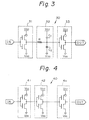
- Figures 1, 2, 3, and 4 show typical existing delay circuits composed of FET's, and to delay the signal, a Schmitt trigger circuit is used in the circuit of Fig. 1 and 2, a network of capacitors and resistors (CR network) is used in the circuit of Fig. 3, and a multistage inverter circuit is used in the circuit of Fig. 4.
- the FET's marked o in the drawings are P-channel FET's.
- the Schmitt trigger circuit 10 is composed of two P-channel FET's 11, 12 and two N-channel FET's 13, 14.
- the P-channel FET 11 and N-channel FET's 13 and 14 are connected in series between a high level constant power supply Vcc and a low level constant power supply Vss.
- the P-channel FET 12 is connected between the high level constant power supply Vcc and a node N2 , which serves as a connecting point for the N-channel FET's 13 and 14.
- the gates of the FET's 11, 12, 13, and 14 are connected to the input terminal IN, and a node N1 is connected to the output terminal OUT of the Schmitt trigger circuit 10.
- the P-channel FET's 11 and 12 are ON (conduction occurs between the source and drain) and the N-channel FET's 13 and 14 are OFF (no conduction occurs between the source and drain), and thus the nodes N1 and N2 are high level.
- the P-channel FET's 11 and 12 become OFF and the N-channel FET 14 becomes ON immediately the input level passes the threshold voltage, but the N-channel FET 13 cannot become ON at the same time because the nodes N1 and N2 are both high level.
- the N-channel FET 13 becomes ON after the node N2 is connected to the low level constant power supply Vss through the N-channel FET 14 and the level thereof becomes low.
- a delay occurs while the node N2 is changed from high level to low level, which supplies the threshold voltage to the gate of FET 13 after the N-channel FET 14 becomes ON.
- the N-channel FET 13 becomes ON, the level of the output terminal OUT is changed from high level to low level. Accordingly, the change of the level from low to high at the input terminal IN is transmitted to the output terminal OUT in the opposite direction at a predetermined interval.
- the Schmitt trigger circuit 20 is composed of two P-channel FET's 21 and 22 and two N-channel FET's 23 and 24.
- the P-channel FET's 21 and 22 and N-channel FET 23 are connected in series between a high level constant power supply Vcc and a low level constant power supply Vss.
- the N-channel FET 24 is connected between the low level constant power supply Vcc and a node N3 which serves as a connecting point for the P-channel FET's 21 and 22.
- the gates of the FET's 21, 22, 23, and 24 are connected to the input terminal IN, and a node N4 is connected to the output terminal OUT of the Schmitt trigger circuit 20.
- the N-channel FET's 23 and 24 are ON and the P-channel FET's 21 and 22 are OFF, and the nodes N3 and N4 are low level.
- the N-channel FET's 22 and 23 immediately become OFF and the P-channel FET 21 becomes ON, but the P-channel FET 22 cannot become ON immediately because the nodes N3 and N4 are both low level. Therefore, the P-channel FET 22 becomes ON after the node N3 is connected to the high level constant power supply Vcc through the P-channel FET 21 and the level thereof becomes high. A delay occurs while that the node N3 is changed from low level to high level after the P-channel FET 21 becomes ON.
- the P-channel FET 22 When the P-channel FET 22 becomes ON, the level of the output terminal OUT is changed from low level to high level, then in the same way as described in Fig. 1, the change of the level from high to low at the input terminal IN is transmitted to the output terminal OUT in the opposite direction at a predetermined interval.
- the delay circuit 30 is composed of two inverters 31 and 33, and a CR network 32.
- Each of the inverters 31 and 33 comprises a P-channel FET and an N-channel FET connected in series between a high level constant power supply Vcc and a low level constant power supply Vss.
- the CR network 32 comprises two capacitors C1 and C2 , and a resistor R.
- the input signal When the input signal is low level, the input signal to the CR network is high level, and accordingly the capacitor C2 is charged and the capacitor C1 is discharged.
- the signal at the output of the inverter 31 When the signal changes from low level to high level at the input terminal IN, the signal at the output of the inverter 31 is changed from high level to low level, thereby discharging the capacitor C2 and charging the capacitor C1.
- the signal input to the CR network 32 is sent to the output of the CR network 32 after a predetermined delay, in accordance with the time constant defined by capacitors C1 and C2 , and the resistor R. This delayed signal is then inverted by the inverter 33.
- the delay operation in this circuit 30 is also carried out, and accordingly, the signal to the input terminal IN is transmitted to the output terminal OUT at a predetermined interval.
- the delay circuit 40 is composed of a multistage inverter, i.e., the delay circuit 40 comprises a plurality of inverters 41, 42, ... 4n.
- Each inverter comprises a P-channel FET and an N-channel FET connected in series between a high level constant power supply Vcc and a low level constant power supply Vss.
- a signal input to the input terminal IN is delayed by each inverter circuit, due to a switching time lag thereof.
- the delay time is defined by the number of inverters in the delay circuit 40.
- the delay operation can be carried out for a one way change of the input signal.
- the Schmitt trigger circuit 10 shown in Fig. 1 delays the input signal only upon a change from low level to high level
- the Schmitt trigger circuit 20 shown in Fig. 2 delays the input signal only upon a change from high level to low level.
- Figures 5A, 5B, and 5C shown waveforms for explaining the operation of the delay circuit as shown in Figs. 1 and 2 when the voltage of the high level constant power supply Vcc is 5 V.
- the waveform indicates a signal input to the input terminal IN of the circuits 10 and 20.
- the input signal changes at time t1 and time t2.
- Fig. 5A the waveform indicates a signal input to the input terminal IN of the circuits 10 and 20. The input signal changes at time t1 and time t2.
- the waveform indicates a signal output from the output terminal OUT of the circuit 10
- Fig. 5C the waveform indicates a signal output from the output terminal OUT of the circuit 20
- Figure 6A, 6B, and 6C show waveforms for explaining the operation of the delay circuit as shown in Figs. 1 and 2 when the voltage of the high level constant power supply Vcc is less than 3 V, for example, 1.5 V.
- the waveform indicates a signal input to the input terminal IN of the circuits 10 and 20. The input signal changes at a time t1 and time t2.
- Fig. 6B the waveform indicates a signal output from the output terminal OUT of the circuit 10, and in Fig.
- the waveform indicates a signal output from the output terminal OUT of the circuit 20. From Figs. 5B, 5C, 6B, and 6C, it is clearly understood that the circuit 10 shown in Fig. 1 delays the input signal only upon a change from low level to high level, and the circuit 20 shown in Fig. 2 delays the input signal only upon a change from high level to low level.
- a delay operation can be carried out for a rising or falling input signal at the input terminal IN, as shown in Figs. 5A and 5D, when the voltage of the high level constant power supply Vcc is 5 V.
- the delay time is not stable when the voltage of the high level constant power supply Vcc is less than 3 V, for example, 1.5 V, because the response of the CR network is blunted under the low voltage condition, as shown in Fig. 6D.
- a wave shaping circuit must be included for compensating the weakened output signal.
- delay circuit is composed of a first switching transistor and a second switching transistor operable in a complementary manner in response to an input signal, an output terminal connected to the node of the first switching transistor and the second switching transistor, one or more switching transistors of the same type as the first switching transistor provided between the first switching transistor and a power source, one or more switching transistors of the same type as the second switching transistor provided between the second switching transistor and another power source, at least one current path connecting at least one pair of nodes, one of which nodes being located between the first switching transistor and the power source and the other node being located between the second switching transistor and the other power source, and one or more capacitors connected to the current path.
- An embodiment of the present invention may provide a delay circuit in which the output signal is delayed by a specified time interval with respect to the input of both a rising edge and a falling edge, and able to work reliably and to obtain a sufficient delay time at a low power source voltage.
- An embodiment of the present invention may provide a small-scale delay circuit having a low power consumption, a stable delay time regardless of changes in the direction of the voltage at the input terminal, and able to operate reliably and to obtain a sufficient delay time at a lower power source voltage.
- FIG. 7 is a circuit diagram of a first embodiment of a delay circuit 50 according to the present invention.
- the delay circuit 50 is composed of two P-channel FET's 51 and 52, two N-channel FET's 53 and 54, two capacitors C3 and C4 , and a resistor R1.
- the P-channel FET's 51 and 52, and N-channel FET's 53 and 54 are connected in series between a high level constant power supply Vcc and a low level constant power supply Vss.
- the gates of the FET's 51, 52, 53, and 54 are connected to an input terminal IN, and a node N5 and a node N7 are connected by a current path 55 having the resistor R1 arranged therein.
- a node N6 is connected to an output terminal OUT. Further, the capacitor C3 is connected to a point in the current path 55, between the node N5 and the resistor R1 , and the capacitor C4 is connected to a point in current path 55 between the node N7 and the resistor R1.
- the free terminal of the capacitor C3 is connected to the high level constant power supply Vcc, and the free terminal of the capacitor C4 is connected to the low level constant power supply Vss.
- MOSFET metal-oxide-semiconductor field effect transistors
- the capacitors C3 and C4 are formed also by MOSFET's by connecting the source and the drain thereof. Namely, if the source and the drain of a MOSFET are connected to the high level constant power supply Vcc and a gate of the MOSFET is connected to the current path 55 between the node N5 and the resistor R1 , the MOSFET acts as the capacitor C3.
- FIG. 8A the signal input to the input terminal IN shown in Fig. 7 is high level "H".
- the P-channel FET's 51 and 52 are OFF, and the N-channel FET's 53 and 54 are ON, and the nodes N5, N6, and N7 are all low level "L", whereby the capacitor C3 is charged and the capacitor C4 is discharged.
- the P-channel FET 51 becomes ON immediately the input level becomes lower than the threshold voltage, and the N-channel FET'S 53 and 54 become OFF immediately the input level becomes lower than the threshold voltage.
- the P-channel FET 52 cannot become ON at this time because the nodes N5 and N6 are still low level.
- the P-channel FET 51 is turned ON, current flows through the FET 51, and a current I1 discharges the capacitor C3 , and at the same time, a current I2 flows through the resistor R1 to charge the capacitor C4.
- the N-channel FET 54 becomes ON immediately the input level exceeds the threshold voltage, and the P-channel FET's 51 and 52 become OFF immediately the input exceeds the threshold voltage.
- the N-channel FET 53 cannot become ON at the same time because the nodes N6 and N7 are both high level.
- the N-channel FET 54 is turned ON, current flow through the FET 54, and a current I3 discharge the capacitor C4 , and at the same time, a current I4 flows through the resistor R1 to charge the capacitor C3.
- Figure 9 is a circuit diagram of a modification of the first embodiment shown in Fig. 7.
- the delay circuit 50 is also composed of two P-channel FET's 51 and 52, two N-channel FET's 53 and 54, two capacitors C3 and C4 , and a resistor R1 , and the connections therebetween are the same as for the delay circuit. 50 shown in Fig. 7, except for the connection of the free terminals of the capacitors C3 and C4.
- the free terminal of the capacitor C3 is connected to the low level constant power supply Vss and the free terminal of the capacitor C4 is connected to the high level constant power supply Vcc in this embodiment, but the free terminal of the capacitor C3 is connected to the high level constant power supply Vcc and the free terminal of the capacitor C4 is connected to the low level constant power supply Vss in Fig. 7.
- the delay operation of the circuit 50′ is the same as the operation of the delay circuit 50 shown in Fig. 7, except that the charge and discharge operations of the capacitors C3 and C4 are reversed.
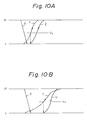
- Figure 10A is a waveform diagram of the delay circuit shown in Figs. 7 and 9, for explaining the operation of the delay circuits when the time constant value decided by the capacitance of the capacitors C3 and C4 and the resistance of the resistor R1 is small.
- Figure 10B is a waveform diagram of the delay circuit shown in Figs. 7 and 9, for explaining the operation of the delay circuits when the time constant value is large.
- the level of the input terminal IN changes from high level "H” to low level “L", as indicated by the reference numeral S in Fig. 10B
- the level of the node N5 slowly changes from low level “L” to high level “H” as indicated by the reference numeral T, in accordance with the large time constant.
- the P-channel FET 52 turns ON when the level of the node N5 exceeds the threshold level V T .
- the level of the output terminal OUT changed from low level "L” to high level “H” as indicated by the reference numeral U at the same speed as that when the time constant value is small.
- Figs. 5A and 5E show waveforms for explaining the operation of the delay circuit of the present invention as shown in Figs. 7 and 9 when the voltage of the high level constant power supply Vcc is 5 V.
- the waveform in Fig. 5E indicates a signal output from the output terminal OUT of the circuit 50 and 50′ when the input signal at the input terminal IN of the circuits 50 and 50′ changes at a time t1 and time t2.
- Figs. 6A to 6F show waveforms for explaining the operation of the delay circuit as shown in Figs. 7 and 9 when the voltage of the high level constant power supply Vcc is less than 3 V, for example, 1.5 V.
- the waveform in Fig. 6E indicates a signal output from the output terminal OUT of the circuit 50 and 50′ when the input signal at the input terminal IN of the circuits 50 and 50, changes at a time t1 and time t2. Comparing Figs. 5E and 6E, it can be clearly understood that the time delay by the delay circuits 50 and 50′ when the voltage of the high level constant power supply Vcc is 1.5 V, is longer than the time delay by the delay circuits 50 and 50′ when the voltage of the high level constant power supply Vcc is 5 V, and from Figs. 5E and 6E, it can be understood that the pulling up time or pulling down time at the delay circuits is almost the same.
- the delay circuit in Fig. 7 and 9 transmits the input signal at the input terminal IN to the output terminal OUT at a predetermined interval when the input signal is rising or falling. Further, the delay circuit in Figs. 7 and 9 requires only the capacitors C3 , C4 and the resistor R1 to obtain a reliable delay time, and thus the circuit is kept to a small scale. Further more, the delay circuit in Figs. 7 and 9 operates effectively when the constant power source Vcc is at a low level.
- FIG 11 is a circuit diagram of a second embodiment of a delay circuit 60 according to the present invention.
- This delay circuit 60 is composed of two P-channel FET's 61 and 62, two N-channel FET's 63 and 64 connected in series between the low level constant power supply Vss and the high level constant power supply Vcc, a current path 65 connecting nodes N8 and N9 , a resistor R2 provided on the current path 65, a capacitor C5 connected to the current path 65 in parallel to the resistor R2 , and a node N9 connected to the output terminal OUT.
- the operation of the delay circuit 60 is almost the same as the operation of the delay circuit 50 shown in Fig. 7, except for the charge and discharge operation of the capacitor C5.
- the signal input to the input terminal IN is high level "H”
- two metal plates of the capacitor C5 are given a negative electric charge because the nodes N5 and N7 are both low level.
- the signal input to the input terminal IN is low level "L”
- the two metal plates of the capacitor C5 are given a positive electric charge because the nodes N5 and N7 are both high level. Accordingly, the charge and discharge operation of the capacitor C5 , which decides the delay time at the delay circuit 60, occurs at the transition of the input signal.
- the waveform-characteristics of the input terminal IN and the output terminal OUT are shown in Figs.
- FIG 12 is a circuit diagram of a third embodiment of a delay circuit 70 according to the present invention.
- This delay circuit 70 is composed of two P-channel FET's 71 and 72, two N-channel FET's 73 and 74 connected in series between the low level constant power supply Vss and the high level constant power supply Vcc, a current path 75 connecting nodes N11 and N13 , resistors R3 and R4 connected in series on the current path 75, a capacitor C6 , and a node N12 connected to the output terminal OUT.
- the capacitor C6 is connected to the current path 75 at the point at which the resistor R3 and R4 are connected thereto, and the free terminal of this capacitor C6 is connected to the high level constant power supply Vcc.
- operation of the delay circuit 70 is almost the same as the operation of the delay circuit 50 shown in Fig. 7, except for charge and discharge operation of the capacitor C6.
- the capacitor C6 When the signal input to the input terminal IN is changed from low level “L” to high level "H", the capacitor C6 is charged because the level of the nodes N11 and N13 is changed from high to low. Accordingly, the charge and discharge operations of the capacitor C6 decides the delay time of the delay circuit 70 in accordance with the time constant decided by the capacitance of the capacitor C6 and the resistance of the resistors R3 and R4.
- Figure 13 is a circuit diagram of a modification of the third embodiment as shown in Fig. 12.
- the construction of the delay circuit 70′ is the same as that of the delay circuit 70 shown in Fig. 12, except for the connection of the free terminal of the capacitor C7. Namely, the free terminal of the capacitor C7 is connected to the low level constant power supply Vss in this embodiment, but is connected to the high level constant power supply Vcc in Fig. 12.
- the operation of the delay circuit 70′ is the same as the operation of the delay circuit 70 shown in Fig. 12, except the charge and discharge operation of the capacitor C7 are reversed.
- FIG 14 is a circuit diagram of a fourth embodiment of a delay circuit according to the present invention.
- This delay circuit 80 is composed of two P-channel FET's 81 and 82, two N-channel FET's 83 and 84 connected in series between the low level constant power supply Vss and the high level constant power supply Vcc, a current path 85 connecting nodes N14 and N16 , capacitors C8 and C9 connected to a different point of the current path 85, and a node N15 connected to the output terminal OUT.
- a free terminal of the capacitor C8 is connected to the high level constant power supply Vcc
- a free terminal of the capacitor C9 is connected to the low level constant power supply Vss. Note, the connection of the free terminals of the capacitors C8 and C9 may be reversed. Since the current path itself has a slight line-resistance, the operation of this delay circuit 80 is the same as that of the delay circuit 50 shown in Fig. 7.
- the following circuits are can be formed: (a) a circuit wherein one of the capacitors C8 or C9 is removed from the delay circuit 80; (b) a circuit wherein one or more resistors are provided on the current path 85 of the circuit in Fig. 14 or the circuit described in (a). Further, the part surrounded by a dot-like Nx may be treated as a common node including the nodes N14 and N16.
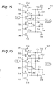
- Figure 15 is a circuit diagram of a fifth embodiment of a delay circuit 90 according to the present invention.
- Three P-channel FET's 91, 92, 93, three N-channel FET's 94, 95, 96, current paths 97 and 98, four capacitors C10 , C11 , C12 , and C13 , and resistors R5 and R6 are used in the delay circuit 90, and the connection of the FET's 92, 93, 94, 95, the current path 97, the capacitors C11 and C12 , and the resistor R6 are the same as for the delay circuit 50 shown in Fig. 7.
- the FET 91 is added between the FET 92 and the high level constant power source Vcc
- the FET 96 is added between the FET 95 and the low level constant power source Vss
- a current path 98 provided with a resistor R5 is added between nodes N17 and N21
- capacitors C10 and C13 are added to the current path 98.
- the operation of the delay circuit 90 is similar to the delay operation described in Fig.
- the FET's 91, 92, and 93 become ON, in this order, at a predetermined interval therebetween them, and when the input signal changes from low level "L” to high level “H”, the FET's 96, 95, and 94 become ON, in this order, also at a predetermined interval therebetween. Accordingly, in the delay circuit 90 shown in Fig. 15, the delay time is longer than that in the delay circuits shown in Figs. 7, 9, 11, 12, 13, and 14.
- Figure 16 shows a delay circuit 90′ as a modifications of the delay circuit 90 shown in Fig. 15.
- the connection of the nodes N17 , N18 , N20 and N21 are different from those of Fig. 15. Namely, in this embodiment, the nodes N17 and N20 are connected by a current path 97′ and the nodes N18 and N21 are connected by a current path 98′.
- the operation of this delay circuit is similar to that of the delay circuit 90 shown in Fig. 15.
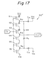
- Figure 17 shows a delay circuit 90 ⁇ as another modification of the delay circuit 90 as shown in Fig. 15.
- the current path 97 and capacitors C11 and C12 are removed from the delay circuit 90 in Fig. 15, and thus the delay time is longer than that in the delay circuit shown in from Figs. 7, 9, 11, 12, 13, and 14 but shorter than that in the delay circuit shown in Figs. 15 and 16.
Landscapes
- Physics & Mathematics (AREA)
- Nonlinear Science (AREA)
- Pulse Circuits (AREA)
- Logic Circuits (AREA)
- Dram (AREA)
- Networks Using Active Elements (AREA)
Applications Claiming Priority (2)
| Application Number | Priority Date | Filing Date | Title |
|---|---|---|---|
| JP63038809A JP2685203B2 (ja) | 1988-02-22 | 1988-02-22 | 遅延回路 |
| JP38809/88 | 1988-02-22 |
Publications (3)
| Publication Number | Publication Date |
|---|---|
| EP0330405A2 true EP0330405A2 (de) | 1989-08-30 |
| EP0330405A3 EP0330405A3 (en) | 1989-11-02 |
| EP0330405B1 EP0330405B1 (de) | 1992-07-08 |
Family
ID=12535616
Family Applications (1)
| Application Number | Title | Priority Date | Filing Date |
|---|---|---|---|
| EP89301628A Expired - Lifetime EP0330405B1 (de) | 1988-02-22 | 1989-02-20 | Verzögerungsschaltung |
Country Status (5)
| Country | Link |
|---|---|
| US (1) | US5097159A (de) |
| EP (1) | EP0330405B1 (de) |
| JP (1) | JP2685203B2 (de) |
| KR (1) | KR930003524B1 (de) |
| DE (1) | DE68901985T2 (de) |
Cited By (5)
| Publication number | Priority date | Publication date | Assignee | Title |
|---|---|---|---|---|
| WO1998012812A1 (de) * | 1996-09-18 | 1998-03-26 | Siemens Aktiengesellschaft | Verzögerungsstufe mit steilen flanken |
| EP0858161A3 (de) * | 1997-02-06 | 1999-11-17 | Nec Corporation | Verzögerungsschaltung mit Pulsformung |
| EP0831586A3 (de) * | 1996-09-18 | 2000-02-23 | Nec Corporation | Variable Verzögerungsschaltung |
| GB2389722B (en) * | 2002-06-13 | 2006-01-11 | Hewlett Packard Development Co | Pulse shaping circuit and method |
| US7239185B2 (en) | 2002-06-13 | 2007-07-03 | Hewlett-Packard Development Company, L.P. | Driver circuit connected to pulse shaping circuitry |
Families Citing this family (11)
| Publication number | Priority date | Publication date | Assignee | Title |
|---|---|---|---|---|
| JP2621612B2 (ja) * | 1990-08-11 | 1997-06-18 | 日本電気株式会社 | 半導体集積回路 |
| JPH0746098A (ja) * | 1993-08-03 | 1995-02-14 | Nec Corp | 遅延回路 |
| JPH0758207A (ja) * | 1993-08-20 | 1995-03-03 | Fujitsu Ltd | データ保持タイミング調整回路及びこれを含む半導体集積回路 |
| JPH08181548A (ja) * | 1994-12-26 | 1996-07-12 | Mitsubishi Electric Corp | 差動増幅回路、cmosインバータ、パルス幅変調方式用復調回路及びサンプリング回路 |
| US5990714A (en) * | 1996-12-26 | 1999-11-23 | United Microelectronics Corporation | Clock signal generating circuit using variable delay circuit |
| JP3586612B2 (ja) * | 2000-03-08 | 2004-11-10 | エルピーダメモリ株式会社 | 遅延回路 |
| US7057450B2 (en) * | 2003-07-30 | 2006-06-06 | Winbond Electronics Corp. | Noise filter for an integrated circuit |
| US7102407B2 (en) * | 2004-03-31 | 2006-09-05 | Intel Corporation | Programmable clock delay circuit |
| CN101057403A (zh) * | 2004-11-15 | 2007-10-17 | 皇家飞利浦电子股份有限公司 | 绝热cmos设计 |
| JP5008032B2 (ja) * | 2007-08-30 | 2012-08-22 | ソニーモバイルディスプレイ株式会社 | 遅延回路、半導体制御回路、表示装置、および電子機器 |
| KR20090126879A (ko) * | 2008-06-05 | 2009-12-09 | 삼성전자주식회사 | 높은 신뢰성과 구동능력을 갖는 드라이버 회로 및 이를구비하는 반도체 메모리 장치 |
Family Cites Families (9)
| Publication number | Priority date | Publication date | Assignee | Title |
|---|---|---|---|---|
| JPS5966220A (ja) * | 1982-10-07 | 1984-04-14 | Shiojiri Kogyo Kk | A/d変換lsi |
| JPS5966219A (ja) * | 1982-10-08 | 1984-04-14 | Oki Electric Ind Co Ltd | V−fコンバ−タ |
| JPH0620176B2 (ja) * | 1982-10-08 | 1994-03-16 | 株式会社日立製作所 | 遅延回路 |
| EP0390226A1 (de) * | 1984-07-31 | 1990-10-03 | Yamaha Corporation | Absorptionsschaltung des Zitterns |
| JPS6153818A (ja) * | 1984-08-23 | 1986-03-17 | Fujitsu Ltd | 遅延回路 |
| US4700089A (en) * | 1984-08-23 | 1987-10-13 | Fujitsu Limited | Delay circuit for gate-array LSI |
| JPS62291215A (ja) * | 1986-06-11 | 1987-12-18 | Hitachi Ltd | 半導体装置 |
| JPS62157420A (ja) * | 1985-12-28 | 1987-07-13 | Toshiba Corp | 遅延回路 |
| JPS648657A (en) * | 1987-06-30 | 1989-01-12 | Mitsubishi Electric Corp | Supplementary semiconductor integrated circuit device |
-
1988
- 1988-02-22 JP JP63038809A patent/JP2685203B2/ja not_active Expired - Lifetime
-
1989
- 1989-02-20 DE DE8989301628T patent/DE68901985T2/de not_active Expired - Fee Related
- 1989-02-20 EP EP89301628A patent/EP0330405B1/de not_active Expired - Lifetime
- 1989-02-21 US US07/312,163 patent/US5097159A/en not_active Expired - Lifetime
- 1989-02-22 KR KR8902064A patent/KR930003524B1/ko not_active Expired - Fee Related
Cited By (7)
| Publication number | Priority date | Publication date | Assignee | Title |
|---|---|---|---|---|
| WO1998012812A1 (de) * | 1996-09-18 | 1998-03-26 | Siemens Aktiengesellschaft | Verzögerungsstufe mit steilen flanken |
| EP0831586A3 (de) * | 1996-09-18 | 2000-02-23 | Nec Corporation | Variable Verzögerungsschaltung |
| US6181183B1 (en) | 1996-09-18 | 2001-01-30 | Siemens Aktiengesellschaft | Steep edge time-delay relay |
| EP0858161A3 (de) * | 1997-02-06 | 1999-11-17 | Nec Corporation | Verzögerungsschaltung mit Pulsformung |
| US6121813A (en) * | 1997-02-06 | 2000-09-19 | Nec Corporation | Delay circuit having a noise reducing function |
| GB2389722B (en) * | 2002-06-13 | 2006-01-11 | Hewlett Packard Development Co | Pulse shaping circuit and method |
| US7239185B2 (en) | 2002-06-13 | 2007-07-03 | Hewlett-Packard Development Company, L.P. | Driver circuit connected to pulse shaping circuitry |
Also Published As
| Publication number | Publication date |
|---|---|
| US5097159A (en) | 1992-03-17 |
| DE68901985T2 (de) | 1993-02-04 |
| JP2685203B2 (ja) | 1997-12-03 |
| EP0330405A3 (en) | 1989-11-02 |
| JPH01213023A (ja) | 1989-08-25 |
| EP0330405B1 (de) | 1992-07-08 |
| KR890013880A (ko) | 1989-09-26 |
| DE68901985D1 (de) | 1992-08-13 |
| KR930003524B1 (en) | 1993-05-01 |
Similar Documents
| Publication | Publication Date | Title |
|---|---|---|
| EP0330405A2 (de) | Verzögerungsschaltung | |
| US4874971A (en) | Edge-sensitive dynamic switch | |
| US5293082A (en) | Output driver for reducing transient noise in integrated circuits | |
| EP0072686B1 (de) | Pufferschaltung mit einer Inverterschaltung | |
| US4532436A (en) | Fast switching circuit | |
| US4450371A (en) | Speed up circuit | |
| US5896043A (en) | Level shift circuit | |
| US5537060A (en) | Output buffer circuit for memory device | |
| KR960011964B1 (ko) | 출력버퍼장치 | |
| EP0086090B1 (de) | Treiberschaltung für kapazitive Lasten | |
| EP0767524A2 (de) | Verfahren und Einrichtung zur Ausgleichung von Stromquellen | |
| US4804869A (en) | BiMOS logical circuit | |
| US5543744A (en) | Driver/receiver circuit for reducing transmission delay | |
| KR20020019390A (ko) | 반도체 집적회로장치 | |
| US5362995A (en) | Voltage comparing circuit | |
| US5489859A (en) | CMOS output circuit with high speed high impedance mode | |
| EP0481698A2 (de) | Dreizustandsschaltkreis | |
| EP0139833A2 (de) | CMOS-Übertragungsschaltung | |
| EP0473409B1 (de) | BiCMOS logische Schaltung | |
| US5406215A (en) | Open drain driver circuit which eliminates overshoot caused by parasitic capacitances | |
| EP0101947B1 (de) | Treiberschaltung | |
| EP0303257A1 (de) | Schaltung zur Erzeugung eines Rücksetzsignals | |
| US5657276A (en) | Output stage for integrated circuits, particularly for electronic memories | |
| US4649290A (en) | Pulse generating circuit | |
| US5530400A (en) | Transistor circuit with transistor characteristic sensor |
Legal Events
| Date | Code | Title | Description |
|---|---|---|---|
| PUAI | Public reference made under article 153(3) epc to a published international application that has entered the european phase |
Free format text: ORIGINAL CODE: 0009012 |
|
| AK | Designated contracting states |
Kind code of ref document: A2 Designated state(s): DE FR GB |
|
| PUAL | Search report despatched |
Free format text: ORIGINAL CODE: 0009013 |
|
| AK | Designated contracting states |
Kind code of ref document: A3 Designated state(s): DE FR GB |
|
| 17P | Request for examination filed |
Effective date: 19891123 |
|
| 17Q | First examination report despatched |
Effective date: 19910328 |
|
| GRAA | (expected) grant |
Free format text: ORIGINAL CODE: 0009210 |
|
| AK | Designated contracting states |
Kind code of ref document: B1 Designated state(s): DE FR GB |
|
| REF | Corresponds to: |
Ref document number: 68901985 Country of ref document: DE Date of ref document: 19920813 |
|
| ET | Fr: translation filed | ||
| PLBE | No opposition filed within time limit |
Free format text: ORIGINAL CODE: 0009261 |
|
| STAA | Information on the status of an ep patent application or granted ep patent |
Free format text: STATUS: NO OPPOSITION FILED WITHIN TIME LIMIT |
|
| 26N | No opposition filed | ||
| REG | Reference to a national code |
Ref country code: GB Ref legal event code: IF02 |
|
| PGFP | Annual fee paid to national office [announced via postgrant information from national office to epo] |
Ref country code: GB Payment date: 20030219 Year of fee payment: 15 |
|
| PG25 | Lapsed in a contracting state [announced via postgrant information from national office to epo] |
Ref country code: GB Free format text: LAPSE BECAUSE OF NON-PAYMENT OF DUE FEES Effective date: 20040220 |
|
| GBPC | Gb: european patent ceased through non-payment of renewal fee |
Effective date: 20040220 |
|
| PGFP | Annual fee paid to national office [announced via postgrant information from national office to epo] |
Ref country code: FR Payment date: 20050208 Year of fee payment: 17 |
|
| PGFP | Annual fee paid to national office [announced via postgrant information from national office to epo] |
Ref country code: DE Payment date: 20050217 Year of fee payment: 17 |
|
| PG25 | Lapsed in a contracting state [announced via postgrant information from national office to epo] |
Ref country code: DE Free format text: LAPSE BECAUSE OF NON-PAYMENT OF DUE FEES Effective date: 20060901 |
|
| REG | Reference to a national code |
Ref country code: FR Ref legal event code: ST Effective date: 20061031 |
|
| PG25 | Lapsed in a contracting state [announced via postgrant information from national office to epo] |
Ref country code: FR Free format text: LAPSE BECAUSE OF NON-PAYMENT OF DUE FEES Effective date: 20060228 |