EP0330971B1 - Circuit de bascule - Google Patents
Circuit de bascule Download PDFInfo
- Publication number
- EP0330971B1 EP0330971B1 EP89102990A EP89102990A EP0330971B1 EP 0330971 B1 EP0330971 B1 EP 0330971B1 EP 89102990 A EP89102990 A EP 89102990A EP 89102990 A EP89102990 A EP 89102990A EP 0330971 B1 EP0330971 B1 EP 0330971B1
- Authority
- EP
- European Patent Office
- Prior art keywords
- inverted
- clock signal
- output
- flip
- data
- Prior art date
- Legal status (The legal status is an assumption and is not a legal conclusion. Google has not performed a legal analysis and makes no representation as to the accuracy of the status listed.)
- Expired - Lifetime
Links
- 230000005669 field effect Effects 0.000 claims description 11
- 238000010586 diagram Methods 0.000 description 4
- 230000010354 integration Effects 0.000 description 4
- 229910001218 Gallium arsenide Inorganic materials 0.000 description 1
- 230000003111 delayed effect Effects 0.000 description 1
- 230000007257 malfunction Effects 0.000 description 1
- 238000012986 modification Methods 0.000 description 1
- 230000004048 modification Effects 0.000 description 1
- 230000001172 regenerating effect Effects 0.000 description 1
Images



Classifications
-
- H—ELECTRICITY
- H03—ELECTRONIC CIRCUITRY
- H03K—PULSE TECHNIQUE
- H03K3/00—Circuits for generating electric pulses; Monostable, bistable or multistable circuits
- H03K3/02—Generators characterised by the type of circuit or by the means used for producing pulses
- H03K3/353—Generators characterised by the type of circuit or by the means used for producing pulses by the use, as active elements, of field-effect transistors with internal or external positive feedback
- H03K3/356—Bistable circuits
- H03K3/356017—Bistable circuits using additional transistors in the input circuit
- H03K3/356052—Bistable circuits using additional transistors in the input circuit using pass gates
- H03K3/35606—Bistable circuits using additional transistors in the input circuit using pass gates with synchronous operation
-
- H—ELECTRICITY
- H03—ELECTRONIC CIRCUITRY
- H03K—PULSE TECHNIQUE
- H03K3/00—Circuits for generating electric pulses; Monostable, bistable or multistable circuits
- H03K3/02—Generators characterised by the type of circuit or by the means used for producing pulses
- H03K3/027—Generators characterised by the type of circuit or by the means used for producing pulses by the use of logic circuits, with internal or external positive feedback
- H03K3/037—Bistable circuits
Definitions
- This invention relates to a high-speed flip-flop circuit possessing functions substantially equivalent to those of a delay flip-flop.
- a delay flip-flop (hereinafter referred to as a D-FF) is in general a circuit that takes in data in synchronization with a clock signal and outputs it at a certain time. At high clock frequencies, this type of D-FF is liable to malfunction in taking in the data.
- Various flip-flop circuits (hereinafter referred to as FF circuits) suitable for high-speed operation have therefore been proposed.
- Fig. 1 is a block diagram showing an example of the configuration of a prior-art FF circuit, known e.g. from IEEE Journal of Solid-State Circuits, vol. SC-22, no. 6, December 1987, pages 1048-1054; K.C. HSIEH et al: "A 12-bit 1-Gword/s GaAs digital - to - analog converter system".
- This FF circuit comprises a pair of master-slave flip-flops (hereinafter referred to as MS-FFs) 1 and 2 for latching data Di and the inverted data D ⁇ i in synchronization with a clock signal CL and its inverted clock signal CL ⁇ , and a selector 3 for selecting the outputs of the MS-FFs 1 and 2 responsive to the clock signal CL and the inverted clock signal CL ⁇ and producing them in the form of data Do and the inverted data D ⁇ o.
- MS-FFs master-slave flip-flops
- the MS-FF 1 is a circuit that latches the data Di and the inverted data D ⁇ i on the rise of the clock signal CL and outputs them on the fall of the clock signal CL, and has an input terminal D1 for input of the data Di, an inverted input terminal D ⁇ 1 for input of the inverted data D ⁇ i, a clock input terminal C1 for input of the clock signal CL, an inverted clock input terminal C ⁇ 1 for input of the inverted clock signal, an output terminal Q1, and an inverted output terminal Q ⁇ 1.
- the MS-FF 2 is a circuit that latches the data Di and the inverted data D ⁇ i on the rise of inverted clock signal CL ⁇ and outputs them on the fall of the inverted clock signal CL ⁇ , and has an input terminal D2 for input of the data Di, an inverted input terminal D ⁇ 2 for input of the inverted data D ⁇ i, a clock input terminal C2 for input of the inverted clock signal CL ⁇ , an inverted clock input terminal C ⁇ 2 for input of the clock signal CL, an output terminal Q2, and an inverted output terminal Q ⁇ 2.
- the selector 3 has an input terminal I1 connected to the output terminal Q1, an inverted input terminal I ⁇ 1 connected to the inverted output terminal Q ⁇ 1, an input terminal I2 connected to the output terminal Q2, an inverted input terminal I ⁇ 2 connected to the inverted output terminal Q ⁇ 2, a control terminal CS for input of the clock signal CL, an inverted control terminal CS ⁇ for input of the inverted clock signal CL ⁇ , an output terminal O for output of the data Do, and an inverted output terminal O ⁇ for output of the inverted data D ⁇ o.
- the selector 3 When the logic level of the control terminal CS is high (hereinafter denoted "H",) and the logic level of the inverted control terminal CS ⁇ is low (hereinafter denoted “L"), the selector 3 produces the logic level of the input terminal I1 at the output terminal O, and produces the logic level of the inverted input terminal I ⁇ 1 at the inverted output terminal O ⁇ ; when the control terminal CS is "L”, and the inverted control terminal CS ⁇ is "H,” it produces the logic level of the input terminal I2 at the output terminal O and the logic level of the inverted input terminal I ⁇ 2 at the inverted output terminal O ⁇ .
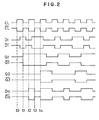
- Fig. 2 is a timing chart for Fig. 1, with times t0 to t4 indicated on the horizontal axis. The operation of Fig. 1 will be explained with reference to this chart.
- the clock signal CL is "H”
- the inverted clock signal is “L”
- the data Di is L
- the inverted data D ⁇ i is “H”
- the output terminal Q1 of the MS-FF 1 is held at “L”
- the inverted output terminal Q ⁇ 1 is held at “H”
- the output terminal Q2 of the MS-FF 2 goes to “L”
- the inverted output terminal Q ⁇ 2 goes to “H”
- the FF circuit in Fig. 1 thus operates as a D-FF by outputting the logic levels of the data Di and the inverted data D ⁇ i when the clock signal CL and the inverted clock signal CL ⁇ change as the data Do and inverted data D ⁇ o at the next change of the clock signal CL and the inverted clock signal CL ⁇ .
- the output signals of the MS-FF 1 are output by the selector 3
- the output signals of the MS-FF 2 are output by the selector 3, so stable, high-speed operation is possible even at high frequencies of the clock signal CL.
- the reason that the FF circuit in Fig. 1 is capable of high-speed operation can be stated as follows.
- the FF circuit in Fig. 1 is constructed so that the MS-FF 1 and the MS-FF 2 operate at only half the clock frequency at which they would operate if used as stand-alone D-FFs.
- the FF circuit in Fig. 1 can therefore operate at a bit rate equal to twice the limiting clock frequency of a stand-alone D-FF.
- From EP-A-0 110 060 is known a flip-flop structure having crossed-coupled inverters of the dynamic type which are driven by a clock pulse (csi).
- a problem with the FF circuit described above is that, since it employs two MS-FFs 1 and 2 and a selector 3, if these comprise NOR gates, for example, eighteen to twenty-two NOR gates are required; the large number of elements required and the complex circuit structure present an obstacle to high levels of circuit integration, and consume more power than the usual D-FF.
- a further problem is that the output is delayed by one bit as compared with the usual D-FF, which restricts the applicability of the circuit.
- An object of the invention is to provide an FF circuit that solves the problem of the large number of elements and complex circuit structure, the problem of large power consumption, and the problem of output delay found in the prior art described above.
- a flip-flop circuit according to the invention is defined in claim 1.
- the first and second transfer gates and the third and fourth transfer gates switch alternately on and off in synchronization with the clock signal and the inverted clock signal and alternately take in the data and the inverted data.
- the first and second inverters and the third and fourth inverters temporarily store, then output, the data and inverted data taken in by the transfer gates.
- the selector alternately outputs the first and second FF outputs in synchronization with the clock signal and inverted clock signal.
- the circuit thus operates, for example, at high speed in the manner of a D-FF. Since the first and second FFs have few elements, the circuit configuration is simplified and can yield improved scales of integration while consuming less power. There is furthermore no one-bit output delay in the configuration of the first and second FFs. The above-mentioned problems can therefore be eliminated.
- the selector circuit can also be simplified by employment of a configuration comprising, for example, six NOR gates. Further embodiments of the invention are defined in the sub-claims
- Fig. 1 is a block diagram of a prior-art FF circuit.
- Fig. 2 is a timing chart for Fig. 1.
- Fig. 3 is a schematic diagram of an FF circuit illustrating an embodiment of this invention.
- Fig. 4 is a timing chart for Fig. 3.
- Fig. 3 is a schematic diagram of an FF circuit illustrating an embodiment of the present invention.
- This FF circuit comprises first and second FFs 10 and 20 for latching input data Di and inverted input data D ⁇ i alternately in synchronization with a clock signal CL and an inverted clock signal CL ⁇ , and a selector 30 for selecting alternately, responsive to the clock signal CL and the inverted clock signal CL ⁇ , the data Di and the inverted data D ⁇ i latched by the first and second FFs 10 and 20 and producing them as data Do and inverted data D ⁇ o; the overall function of this FF circuit is to operate as a D-FF.
- the first FF 10 comprises a first transfer gate 11 which is in the form of a field effect transistor, which has one of its source/drain electrodes connected to an input data terminal, which is also denoted by Di, to receive the data Di, whose gate electrode is connected to a clock signal input terminal CL so that it turns on and off responsive to the clock signal CL and which, when it is on, takes in the data Di.
- a first transfer gate 11 which is in the form of a field effect transistor, which has one of its source/drain electrodes connected to an input data terminal, which is also denoted by Di, to receive the data Di, whose gate electrode is connected to a clock signal input terminal CL so that it turns on and off responsive to the clock signal CL and which, when it is on, takes in the data Di.
- the first FF 10 also comprises a second transfer gate 12 which is in the form of a field effect transistor, which has one of its source/drain electrodes connected to an inverted input data terminal D ⁇ i to receive the inverted data D ⁇ i, which turns on and off responsive to the clock signal CL and which, when it is on, takes in the inverted data D ⁇ i.
- the other of the source/drain electrodes of the transfer gate 11 is connected to an output node N11 of the flip-flop circuit 10.
- the other of the source/drain electrodes of the transfer gate 12 is connected to an output node N12 of the flip-flop circuit 10.
- the first FF 10 further comprises a latch circuit 15 comprising first and second inverters 13 and 14 which are cross-coupled across the output nodes N11 and N12 of the first and second transfer gates 11 and 12, as illustrated in Fig. 3. More specifically, the first inverter 13 has input and output nodes connected to the outputs of the first and second transfer gates 11 and 12, respectively. The second inverter 14 has input and output nodes connected to the outputs of the second and first transfer gates 12 and 11, respectively.
- the second FF 20 comprises a third transfer gate 21 which is in the form of a field effect transistor, which has one of its source/drain electrodes connected to the input data terminal Di to receive the data Di, whose gate electrode is connected to an inverted clock signal input terminal CL ⁇ so that it turns on and off responsive to the inverted clock signal CL ⁇ and which, when it is on, takes in the data Di.
- a third transfer gate 21 which is in the form of a field effect transistor, which has one of its source/drain electrodes connected to the input data terminal Di to receive the data Di, whose gate electrode is connected to an inverted clock signal input terminal CL ⁇ so that it turns on and off responsive to the inverted clock signal CL ⁇ and which, when it is on, takes in the data Di.
- the second FF 20 also comprises a fourth transfer gate 22 which is in the form of a field effect transistor, which has one of its source/drain electrodes connected to the inverted input data terminal D ⁇ i to receive the data D ⁇ i, whose gate electrode is connected to the inverted clock signal input terminal CL ⁇ so that it turns on and off responsive to the inverted clock signal CL ⁇ and which, when it is on, takes in the data Di ⁇ .
- a fourth transfer gate 22 which is in the form of a field effect transistor, which has one of its source/drain electrodes connected to the inverted input data terminal D ⁇ i to receive the data D ⁇ i, whose gate electrode is connected to the inverted clock signal input terminal CL ⁇ so that it turns on and off responsive to the inverted clock signal CL ⁇ and which, when it is on, takes in the data Di ⁇ .
- the second FF 20 further comprises a latch circuit 25 comprising third and fourth inverters 23 and 24 which are cross-coupled across the output nodes N21 and N22 of the third and fourth transfer gates 21 and 22. More specifically, the third inverter 23 has input and output nodes connected to the outputs of the third and fourth transfer gates 21 and 22, respectively. The fourth inverter 24 has input and output nodes connected to the outputs of the fourth and third transfer gates 24 and 23, respectively.
- the first to fourth transfer gates 11, 12, 21, and 22 which comprise field-effect transistors (hereinafter referred to as FETs) turn on when the clock signal CL and inverted clock signal CL ⁇ applied to their gate electrodes are "H,” and turn off when they are "L.”
- FETs field-effect transistors
- the selector 30 comprises first to sixth two-input NOR gates 31, 32, 33, 34, 35, and 36; the clock signal CL and the node N11 are connected to the inputs of the first NOR gate 31, the clock signal CL and the node N12 to the inputs of the second NOR gate 32, the inverted clock signal CL ⁇ and the node N21 to the inputs of the third NOR gate 33, and the inverted clock signal CL ⁇ and the node N22 to the inputs of the fourth NOR gate 34.
- the output nodes N31 and N33 of the first and third NOR gates 31 and 33 are connected to the inputs of the fifth NOR gate 35, the output nodes N32 and N34 of the second and fourth NOR gates 32 and 34 are connected to the inputs of the sixth NOR gate 36, and the data Do and inverted data D ⁇ o are output from the outputs of the fifth and sixth NOR gates 35 and 36.
- Fig. 4 is a timing chart for Fig. 3, with times t0 to t4 indicated on the horizontal axis. The operation of Fig. 3 will be explained with reference to this chart.
- the data Di is "L”
- the inverted data D ⁇ i is “H”
- the clock signal CL rises to “H”
- the inverted clock signal CL ⁇ falls to “L”
- the first and second transfer gates 11 and 12 turn on
- the output node N11 goes to “L”
- the output node N12 goes to “H”
- the third and fourth transfer gates 21 and 22 turn off, and the output nodes N21 and N22 retain their previous “L” and “H” states, respectively.
- the data Di rises to "H,” and the inverted data D ⁇ i falls to “L.” Accordingly, the node N11 rises to "H,” and the node N12 falls to “L.” Because the clock signal CL is "H,” the nodes N31 and N32 are kept at “L.”
- the data Di falls to "L,” and the inverted data D ⁇ i rises to “H.” Accordingly, the node N21 falls to “L,” and the node N22 rises to “H.” Because the inverted clock signal CL ⁇ is "H,” the nodes N33 and N34 are kept at “L.”
- the data Di rises to "H,” and the inverted data D ⁇ i falls to “L.” Accordingly, the node N11 rises to "H,” and the node N12 falls to “L.” Because the clock signal CL is "H,” the nodes N31 and N32 are kept at “L.”
- the selector 30 produces the outputs of the second FF 20, namely the signals at the nodes N21 and N22, as the data Do and the inverted data D ⁇ o; when the clock signal CL goes to "L” and the inverted clock signal CL ⁇ goes to "H,” it produces the outputs of the first FF 10, namely the signals at the nodes N11 and N12, as the data Do and the inverted data D ⁇ o.
- the selector 30 can comprise other logic circuit of the same function. Moreover, it can comprises two pairs of transfer gates controlled by the clock signal CL and the inverted clock signal CL ⁇ , and selectively transfer the outputs of the nodes N11 and N12, or the nodes N21 and N22, to the output nodes Do and D ⁇ o.
- the first and second FFs according to this invention comprise two transfer gates and two inverters apiece, the number of elements is small, power consumption can be accordingly reduced, and the circuit structure can be simplified, permitting a higher scale of integration. There is furthermore no one-bit output delay as in the prior art; the removal of this restriction enables many applications.
Landscapes
- Shift Register Type Memory (AREA)
- Dram (AREA)
Claims (6)
- Bascule bistable constituée de première et seconde bascules (10, 20), ayant chacune des première et seconde bornes de sortie (N11, N12, N21, N22) , respectives,ladite première bascule (10) étant connectée de manière à verrouiller la donnée d'entrée (Di) et la donnée d'entrée inversée (Di) en synchronisation avec un signal d'horloge (CL), et de manière à engendrer un premier signal de sortie et un premier signal de sortie inversé au niveau de ladite première borne de sortie (N11) et de ladite seconde borne de sortie (N12) de ladite première bascule (10),ladite seconde bascule (20) étant connectée de manière à verrouiller ladite donnée d'entrée (Di) et ladite donnée d'entrée inversée (

 un circuit sélecteur (30), connecté auxdites première et seconde bascules (10, 20), pour sélectionner et restituer ledit premier signal de sortie et ledit premier signal de sortie inversé en réponse audit signal d'horloge (CL) et sélectionner et restituer ledit second signal de sortie et ledit second signal de sortie inversé en réponse audit signal d'horloge inversé (
 caractérisée ce queladite première bascule (10) comportedes première et deuxième portes de transfert (11, 12) connectées pour recevoir directement ladite donnée d'entrée (Di) et ladite donnée d'entrée inversée (
 dans laquelle ladite seconde bascule (20) comporte des troisième et quatrième portes de transfert (21, 22) connectées pour recevoir directement ladite donnée (Di) et ladite donnée inversée (

- Bascule bistable selon la revendication 1, dans laquelleledit circuit sélecteur (30) est adapté pour sélectionner ledit premier signal de sortie et ledit premier signal de sortie inversé lorsque ledit signal d'horloge est à un niveau bas, etledit circuit sélecteur (30) est adapté pour sélectionner ledit second signal de sortie et ledit second signal de sortie inversé lorsque ledit signal d'horloge inversé est à un niveau bas.
- Bascule bistable selon la revendication 1, dans laquelle ledit circuit sélecteur comporte des première et deuxième portes NON-OU (31, 32) destinées à traiter les signaux de sortie desdites première et deuxième portes de transfert (11, 12) en utilisant ledit signal d'horloge, des troisième et quatrième portes NON-OU (33, 34) destinées à traiter les signaux de sortie desdites troisième et quatrième portes de transfert (21, 22) en utilisant ledit signal d'horloge inversé, une cinquième porte NON-OU (35) destinée à traiter les sorties desdites première et troisième portes NON-OU, et une sixième porte NON-OU (36) destinée à traiter les sorties desdites deuxième et quatrième portes NON-OU.
- Bascule bistable selon la revendication 1, dans laquelleledit premier signal de sortie et ledit premier signal de sortie inversé de ladite première bascule sont les sorties desdites première et deuxième portes de transfert (11, 12), etledit second signal de sortie et ledit second signal de sortie inversé de ladite seconde bascule sont les sorties desdites troisième et quatrième portes de transfert (21, 22).
- Bascule bistable selon la revendication 1, dans laquelleledit premier inverseur (13) a ses bornes d'entrée et de sortie qui sont connectées. aux sorties desdites première et deuxième portes de transfert (11, 12), respectivement,ledit deuxième inverseur (14) a ses bornes d'entrée et de sortie qui sont connectées aux sorties desdites deuxième et première portes de transfert (12, 11), respectivement,ledit troisième inverseur (23) a ses bornes d'entrée et de sortie qui sont connectées aux sorties desdites troisième et quatrième portes de transfert (21, 22), respectivement, etledit quatrième inverseur (24) a ses bornes d'entrée et de sortie qui sont connectées aux sorties desdites quatrième et troisième portes de transfert (22, 21), respectivement.
- Bascule bistable selon la revendication 1, dans laquelleladite première porte de transfert (11) est constituée d'un premier transistor à effet de champ dont l'une des électrodes de source/drain est connectée pour recevoir ladite donnée d'entrée (Di) et dont l'autre des électrodes de source/drain constitue ladite borne de sortie (N11) de ladite première porte de transfert (11),ladite deuxième porte de transfert (12) est constituée d'un second transistor à effet de champ dont l'une des électrodes de source/drain est connectée pour recevoir ladite donnée d'entrée inversée (
 les électrodes de grille desdits premier et second transistors à effet de champ sont connectées pour recevoir ledit signal d'horloge (CL),ladite troisième porte de transfert (21) est constituée d'un transistor à effet de champ dont l'une des électrodes de source/drain est connectée pour recevoir ladite donnée d'entrée (Di) et dont l'autre des électrodes de source/drain constitue ladite borne de sortie (N21) de ladite troisième porte de transfert (21),ladite quatrième porte de transfert (22) est constituée d'un quatrième transistor à effet de champ dont l'une des électrodes de source/drain est connectée pour recevoir ladite donnée d'entrée inversée (
 les électrodes de grille desdits troisième et quatrième transistors à effet de champ sont connectées pour recevoir ledit signal d'horloge inversé (
Applications Claiming Priority (2)
| Application Number | Priority Date | Filing Date | Title |
|---|---|---|---|
| JP63047047A JPH077901B2 (ja) | 1988-02-29 | 1988-02-29 | フリップフロップ回路 |
| JP47047/88 | 1988-02-29 |
Publications (3)
| Publication Number | Publication Date |
|---|---|
| EP0330971A2 EP0330971A2 (fr) | 1989-09-06 |
| EP0330971A3 EP0330971A3 (fr) | 1991-04-24 |
| EP0330971B1 true EP0330971B1 (fr) | 1996-05-22 |
Family
ID=12764255
Family Applications (1)
| Application Number | Title | Priority Date | Filing Date |
|---|---|---|---|
| EP89102990A Expired - Lifetime EP0330971B1 (fr) | 1988-02-29 | 1989-02-21 | Circuit de bascule |
Country Status (5)
| Country | Link |
|---|---|
| US (1) | US5025174A (fr) |
| EP (1) | EP0330971B1 (fr) |
| JP (1) | JPH077901B2 (fr) |
| CA (1) | CA1299682C (fr) |
| DE (1) | DE68926518T2 (fr) |
Families Citing this family (20)
| Publication number | Priority date | Publication date | Assignee | Title |
|---|---|---|---|---|
| US5140180A (en) * | 1990-08-24 | 1992-08-18 | Ncr Corporation | High speed cmos flip-flop employing clocked tristate inverters |
| US5414380A (en) * | 1993-04-19 | 1995-05-09 | Motorola, Inc. | Integrated circuit with an active-level configurable and method therefor |
| US5508648A (en) * | 1994-08-01 | 1996-04-16 | Intel Corporation | Differential latch circuit |
| JP3043241B2 (ja) * | 1994-10-24 | 2000-05-22 | 沖電気工業株式会社 | 可変遅延回路 |
| US5650735A (en) * | 1995-03-24 | 1997-07-22 | Texas Instruments Incorporated | Low power, high performance latching interfaces for converting dynamic inputs into static outputs |
| US5638018A (en) * | 1995-06-02 | 1997-06-10 | Advanced Micro Devices, Inc. | P-type flip-flop |
| USH1796H (en) * | 1996-05-02 | 1999-07-06 | Sun Microsystems, Inc. | Method and circuit for eliminating hold time violations in synchronous circuits |
| JPH09312553A (ja) * | 1996-05-22 | 1997-12-02 | Nec Corp | 論理回路 |
| JPH10117127A (ja) * | 1996-10-11 | 1998-05-06 | Toshiba Corp | 論理記憶回路及び論理回路 |
| US6069839A (en) * | 1998-03-20 | 2000-05-30 | Cypress Semiconductor Corp. | Circuit and method for implementing single-cycle read/write operation(s), and random access memory including the circuit and/or practicing the method |
| US6232796B1 (en) * | 1999-07-21 | 2001-05-15 | Rambus Incorporated | Apparatus and method for detecting two data bits per clock edge |
| US6417711B2 (en) * | 1999-10-19 | 2002-07-09 | Honeywell Inc. | High speed latch and flip-flop |
| US6563356B2 (en) | 1999-10-19 | 2003-05-13 | Honeywell International Inc. | Flip-flop with transmission gate in master latch |
| US6617901B1 (en) * | 2001-04-27 | 2003-09-09 | Cypress Semiconductor Corp. | Master/dual-slave D type flip-flop |
| US6700425B1 (en) | 2001-10-30 | 2004-03-02 | Integrated Device Technology, Inc. | Multi-phase clock generators that utilize differential signals to achieve reduced setup and hold times |
| US6573775B2 (en) | 2001-10-30 | 2003-06-03 | Integrated Device Technology, Inc. | Integrated circuit flip-flops that utilize master and slave latched sense amplifiers |
| US7525362B1 (en) * | 2006-03-17 | 2009-04-28 | Xilinx, Inc. | Circuit for and method of preventing an error in a flip-flop |
| US7855587B1 (en) | 2006-06-02 | 2010-12-21 | Marvell International Ltd. | Asymmetric sense-amp flip-flop |
| US8754692B2 (en) * | 2008-09-04 | 2014-06-17 | Oracle America, Inc. | Low power and soft error hardened dual edge triggered flip flop |
| US8149643B2 (en) | 2008-10-23 | 2012-04-03 | Cypress Semiconductor Corporation | Memory device and method |
Citations (1)
| Publication number | Priority date | Publication date | Assignee | Title |
|---|---|---|---|---|
| EP0110060A1 (fr) * | 1982-11-01 | 1984-06-13 | International Business Machines Corporation | Circuit FET pour changer le niveau de tension |
Family Cites Families (3)
| Publication number | Priority date | Publication date | Assignee | Title |
|---|---|---|---|---|
| DE2834798C3 (de) * | 1978-08-09 | 1981-07-16 | Standard Elektrik Lorenz Ag, 7000 Stuttgart | Schaltungsanordnung zum Ansteuern einflankengesteuerter Bauelemente |
| US4825409A (en) * | 1985-05-13 | 1989-04-25 | Wang Laboratories, Inc. | NMOS data storage cell for clocked shift register applications |
| JPS61283092A (ja) * | 1985-06-06 | 1986-12-13 | Mitsubishi Electric Corp | リセツトあるいはセツト付記憶回路を有した半導体集積回路 |
-
1988
- 1988-02-29 JP JP63047047A patent/JPH077901B2/ja not_active Expired - Fee Related
-
1989
- 1989-02-21 DE DE68926518T patent/DE68926518T2/de not_active Expired - Fee Related
- 1989-02-21 US US07/313,077 patent/US5025174A/en not_active Expired - Fee Related
- 1989-02-21 EP EP89102990A patent/EP0330971B1/fr not_active Expired - Lifetime
- 1989-02-23 CA CA000591937A patent/CA1299682C/fr not_active Expired - Fee Related
Patent Citations (1)
| Publication number | Priority date | Publication date | Assignee | Title |
|---|---|---|---|---|
| EP0110060A1 (fr) * | 1982-11-01 | 1984-06-13 | International Business Machines Corporation | Circuit FET pour changer le niveau de tension |
Non-Patent Citations (1)
| Title |
|---|
| E.A.ZUIDERVEEN: "Handbuch der digitalen Schaltungen", Franzis', Munich, Germany, 1981, pages 208 and 209 * |
Also Published As
| Publication number | Publication date |
|---|---|
| JPH01221911A (ja) | 1989-09-05 |
| US5025174A (en) | 1991-06-18 |
| JPH077901B2 (ja) | 1995-01-30 |
| CA1299682C (fr) | 1992-04-28 |
| DE68926518T2 (de) | 1997-01-23 |
| EP0330971A3 (fr) | 1991-04-24 |
| EP0330971A2 (fr) | 1989-09-06 |
| DE68926518D1 (de) | 1996-06-27 |
Similar Documents
| Publication | Publication Date | Title |
|---|---|---|
| US5025174A (en) | Flip-flop circuit | |
| US6753714B2 (en) | Reducing power and area consumption of gated clock enabled flip flops | |
| CA1258498A (fr) | Reseau logique programmable cmos | |
| EP0502732B1 (fr) | Générateur d'impulsions | |
| US5406216A (en) | Technique and method for asynchronous scan design | |
| EP1460760A1 (fr) | Bascule à double front raide avec réinitialisation asynchrone programmable | |
| US5543731A (en) | Dynamic and preset static multiplexer in front of latch circuit for use in static circuits | |
| US6573775B2 (en) | Integrated circuit flip-flops that utilize master and slave latched sense amplifiers | |
| US3679913A (en) | Binary flip-flop employing insulated gate field effect transistors and suitable for cascaded frequency divider operation | |
| US5907589A (en) | GHZ range frequency divider in CMOS | |
| US5072132A (en) | Vsli latch system and sliver pulse generator with high correlation factor | |
| US4933571A (en) | Synchronizing flip-flop circuit configuration | |
| EP0793342A2 (fr) | Circuit de bascule | |
| US5212411A (en) | Flip-flop circuit having cmos hysteresis inverter | |
| JP3299290B2 (ja) | 高速cmosフリップフロップ | |
| KR101629231B1 (ko) | 데이터 홀드 기능을 갖는 도미노 로직 블록 및 그것을 구비한 도미노 로직 | |
| JP2831788B2 (ja) | フリップフロップ回路 | |
| US20050280449A1 (en) | Apparatus and method for high frequency state machine divider with low power consumption | |
| US5793672A (en) | Low power register memory element circuits | |
| JP2560698B2 (ja) | ラツチ回路 | |
| US4988896A (en) | High speed CMOS latch without pass-gates | |
| US4771187A (en) | Bistable circuit | |
| JPH0551209B2 (fr) | ||
| KR100249019B1 (ko) | 주파수 분주회로 | |
| JP2575834B2 (ja) | フリップフロップ回路 |
Legal Events
| Date | Code | Title | Description |
|---|---|---|---|
| PUAI | Public reference made under article 153(3) epc to a published international application that has entered the european phase |
Free format text: ORIGINAL CODE: 0009012 |
|
| AK | Designated contracting states |
Kind code of ref document: A2 Designated state(s): DE FR GB |
|
| PUAL | Search report despatched |
Free format text: ORIGINAL CODE: 0009013 |
|
| AK | Designated contracting states |
Kind code of ref document: A3 Designated state(s): DE FR GB |
|
| 17P | Request for examination filed |
Effective date: 19910819 |
|
| 17Q | First examination report despatched |
Effective date: 19931116 |
|
| GRAA | (expected) grant |
Free format text: ORIGINAL CODE: 0009210 |
|
| AK | Designated contracting states |
Kind code of ref document: B1 Designated state(s): DE FR GB |
|
| ET | Fr: translation filed | ||
| REF | Corresponds to: |
Ref document number: 68926518 Country of ref document: DE Date of ref document: 19960627 |
|
| GRAH | Despatch of communication of intention to grant a patent |
Free format text: ORIGINAL CODE: EPIDOS IGRA |
|
| PLBE | No opposition filed within time limit |
Free format text: ORIGINAL CODE: 0009261 |
|
| STAA | Information on the status of an ep patent application or granted ep patent |
Free format text: STATUS: NO OPPOSITION FILED WITHIN TIME LIMIT |
|
| 26N | No opposition filed | ||
| PGFP | Annual fee paid to national office [announced via postgrant information from national office to epo] |
Ref country code: GB Payment date: 19980212 Year of fee payment: 10 |
|
| PG25 | Lapsed in a contracting state [announced via postgrant information from national office to epo] |
Ref country code: GB Free format text: LAPSE BECAUSE OF NON-PAYMENT OF DUE FEES Effective date: 19990221 |
|
| GBPC | Gb: european patent ceased through non-payment of renewal fee |
Effective date: 19990221 |
|
| PGFP | Annual fee paid to national office [announced via postgrant information from national office to epo] |
Ref country code: DE Payment date: 20060216 Year of fee payment: 18 |
|
| PG25 | Lapsed in a contracting state [announced via postgrant information from national office to epo] |
Ref country code: DE Free format text: LAPSE BECAUSE OF NON-PAYMENT OF DUE FEES Effective date: 20070901 |
|
| PGFP | Annual fee paid to national office [announced via postgrant information from national office to epo] |
Ref country code: FR Payment date: 20070208 Year of fee payment: 19 |
|
| REG | Reference to a national code |
Ref country code: FR Ref legal event code: ST Effective date: 20081031 |
|
| PG25 | Lapsed in a contracting state [announced via postgrant information from national office to epo] |
Ref country code: FR Free format text: LAPSE BECAUSE OF NON-PAYMENT OF DUE FEES Effective date: 20080229 |