EP0331282A1 - Sonde de test pour circuits imprimés avec des contacts positionnés de façon exacte sur la base d'une membrane - Google Patents
Sonde de test pour circuits imprimés avec des contacts positionnés de façon exacte sur la base d'une membrane Download PDFInfo
- Publication number
- EP0331282A1 EP0331282A1 EP89300688A EP89300688A EP0331282A1 EP 0331282 A1 EP0331282 A1 EP 0331282A1 EP 89300688 A EP89300688 A EP 89300688A EP 89300688 A EP89300688 A EP 89300688A EP 0331282 A1 EP0331282 A1 EP 0331282A1
- Authority
- EP
- European Patent Office
- Prior art keywords
- membrane
- region
- contacts
- translation stage
- central
- Prior art date
- Legal status (The legal status is an assumption and is not a legal conclusion. Google has not performed a legal analysis and makes no representation as to the accuracy of the status listed.)
- Granted
Links
- 239000012528 membrane Substances 0.000 title claims abstract description 62
- 238000012360 testing method Methods 0.000 title abstract description 41
- 239000000523 sample Substances 0.000 title abstract description 33
- 238000013519 translation Methods 0.000 claims abstract description 44
- 238000000034 method Methods 0.000 claims abstract description 19
- 239000000463 material Substances 0.000 claims description 5
- 230000002093 peripheral effect Effects 0.000 claims description 5
- 238000003825 pressing Methods 0.000 claims description 2
- 238000006073 displacement reaction Methods 0.000 abstract description 8
- 239000013589 supplement Substances 0.000 abstract 1
- 238000004519 manufacturing process Methods 0.000 description 6
- 235000012431 wafers Nutrition 0.000 description 5
- 238000004026 adhesive bonding Methods 0.000 description 4
- 238000005516 engineering process Methods 0.000 description 4
- 230000013011 mating Effects 0.000 description 4
- 239000004065 semiconductor Substances 0.000 description 3
- 230000009471 action Effects 0.000 description 2
- 230000005489 elastic deformation Effects 0.000 description 2
- 238000004806 packaging method and process Methods 0.000 description 2
- 238000012545 processing Methods 0.000 description 2
- 239000004642 Polyimide Substances 0.000 description 1
- 238000013459 approach Methods 0.000 description 1
- 230000015572 biosynthetic process Effects 0.000 description 1
- 239000004020 conductor Substances 0.000 description 1
- 230000008878 coupling Effects 0.000 description 1
- 238000010168 coupling process Methods 0.000 description 1
- 238000005859 coupling reaction Methods 0.000 description 1
- 230000003247 decreasing effect Effects 0.000 description 1
- 238000001514 detection method Methods 0.000 description 1
- 239000010408 film Substances 0.000 description 1
- 239000003292 glue Substances 0.000 description 1
- 238000010348 incorporation Methods 0.000 description 1
- 239000012212 insulator Substances 0.000 description 1
- 238000002955 isolation Methods 0.000 description 1
- 239000002184 metal Substances 0.000 description 1
- 238000003801 milling Methods 0.000 description 1
- 238000012986 modification Methods 0.000 description 1
- 230000004048 modification Effects 0.000 description 1
- 238000000059 patterning Methods 0.000 description 1
- 238000000206 photolithography Methods 0.000 description 1
- 238000007747 plating Methods 0.000 description 1
- 229920001721 polyimide Polymers 0.000 description 1
- 230000008569 process Effects 0.000 description 1
- 238000009877 rendering Methods 0.000 description 1
- 229910052710 silicon Inorganic materials 0.000 description 1
- 239000010703 silicon Substances 0.000 description 1
- 238000004544 sputter deposition Methods 0.000 description 1
- 239000010409 thin film Substances 0.000 description 1
- 230000000007 visual effect Effects 0.000 description 1
Images

Classifications
-
- G—PHYSICS
- G01—MEASURING; TESTING
- G01R—MEASURING ELECTRIC VARIABLES; MEASURING MAGNETIC VARIABLES
- G01R1/00—Details of instruments or arrangements of the types included in groups G01R5/00 - G01R13/00 and G01R31/00
- G01R1/02—General constructional details
- G01R1/06—Measuring leads; Measuring probes
- G01R1/067—Measuring probes
- G01R1/073—Multiple probes
- G01R1/07307—Multiple probes with individual probe elements, e.g. needles, cantilever beams or bump contacts, fixed in relation to each other, e.g. bed of nails fixture or probe card
- G01R1/0735—Multiple probes with individual probe elements, e.g. needles, cantilever beams or bump contacts, fixed in relation to each other, e.g. bed of nails fixture or probe card arranged on a flexible frame or film
Definitions
- the present invention relates to test probes for testing integrated circuits.
- a major objective of the present invention is to provide a test probe with more precisely controlled contact registration and a method of making the same.
- Semiconductor processing technology has provided for the manufacture of small, complex integrated circuits. These integrated circuits can be processed in batches on a single semiconductor wafer. The cost of fabricating an integrated circuit is low relative to the cost of packaging individual devices and integrating them into systems. Depending on circuit complexity and the processing technology employed, the manufacturing yield for a device can vary considerably, e.g., from 0% to 100% of devices on a wafer may be fully functional.
- test instruments Since it is costly to test an integrated circuit after packaging, and even more costly to test after incorporation of a packaged integrated circuit into a system, test instruments have been designed to test integrated circuits while still on the wafers on which they were fabricated. Typically, test probes physically and electrically contact bonding pads on an integrated circuit to provide the electrically coupling required for evaluating its functionality.
- Test probes have had to evolve to keep pace with rapidly advancing integrated circuit technology.
- Tests probes have been designed with wires cantilevered radially inward and downward to contact bonding pads on an integrated circuit die. Typically, these are the same bonding pads used to couple the die electrically with a package which protects and provides interfacing for the integrated circuit. It has not proved practicable to develop wire-based probes with sufficiently thin and numerous wires to test today's most highly integrated circuits.
- a carrier board can be glued to the membrane.
- An annular translation stage is positioned within the carrier board and frictionally contacts an annular membrane region enclosing the contacts. The translation stage is pushed against the membrane so that the region enclosed by the translation stage protrudes relative to the carrier board. This ensures that the contacts can contact the bonding pads of the die without physical interference caused by contact of the membrane with areas of the wafer away from the die under test.
- a lens assembly with an elastomeric spring is pressed against the contact region of the membrane to force the contacts against the pads during testing.
- a window is situated to confine the lens assembly, pressing it against the membrane, and to provide for visual alignment of contacts and pads.
- the present invention provides for the constraint of relative movement between contacts during the protrusion of the translation stage. This is done primarily by bonding the translation stage to the membrane so that the membrane region enclosed by the translation stage stretches less than the region outside the translation stage during its protrusion.
- This approach can be supplemented by forming a rigid pattern within a central region extending near but excluding the contacts on the membrane. This pattern can be dedicated to maintaining contact positions only, or serve an additional purpose such as height sensing or probe alignment.
- the contacts can be positioned initially to precompensate for subsequent relative movements.
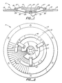
- a membrane-based test probe 11 comprises a membrane 13, a carrier 14, an insulator ring 16, a translation stage 17, a lens assembly 19 and an alignment window 21, as shown in FIGS. 1 and 2.
- Fabricated on membrane 13 are contacts 23 and associated leads 25, shown in FIGS.2 and 3. Contacts 23 are positioned to mate with bonding pads on an integrated circuit die. The electrical functionality of the die can be tested by a circuit analyzer using test probe 11 as an interface.
- the die under test is one of many fabricated on a wafer of silicon or other semiconductor material.
- its center is protruded by translation stage 17 from the plane defined by carrier 15.
- the position of translation stage 17 relative to carrier 15 is maintained by three leaf springs 27.
- Translation stage 17 encircles and maintains the protruded position for the membrane's inner region 29, which bears contacts 23, and the membrane's central region 31, which is radially inward of contacts 23, as shown in FIG. 3.
- Translation stage 17 is used to protrude inner region 29 and central region 31 from their positions prior to translation. Membrane 13 necessarily stretches to accommodate this protrusion. As shown in FIG. 3, translation stage 17 is bonded to membrane 13 with glue 33 along an annular region 35 of membrane 13. Translation stage 17 is considerably less flexible than membrane 13 and thus constrains expansion of regions 29 and 31 enclosed by it. Stretching to accommodate protrusion is thus largely confined to an outer region 37 of membrane 13 between annular region 35 to which translation stage 17 is glued and a peripheral region 39, FIG. 1, of membrane 13 to which carrier 15 is glued.
- contacts 23 formed thereon substantially maintain their original positions during and after the translation procedure. Without such constraint, contacts 23 would not only move, but move in relatively unpredictable amounts since, generally, the elastic deformation forced by the protrusion would be non-uniform.
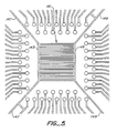
- FIG. 4 shows a rectangular pattern 41 formed in central region 31.
- This pattern 41 can be formed conveniently in the same steps used in defining leads 25. Being a closed pattern of material more rigid than membrane 13, rectangular pattern 41 serves to further constrain the movement of contacts 23 from the membrane center and relative to each other during protrusion.
- rectangular includes “square” as a special case.
- a central pattern 141 serves a function other than dimensional stability.
- the basically rectangular center pattern 141 comprises two capacitively coupled interdigitated electrical elements 143 and 145.
- Each element 143, 145 has an associated pair of leads 147, 149.
- Element 143 is used as a signal source and its leads 147 are used to provide a sine wave input to pattern 141.
- Element 145 is used as a signal sensor and its lead 149 transmit a detected signal to a signal strength detector (not shown).
- Signal amplitude is at a minimum in the absence of a device under test. As a die is raised toward the contacts, capacitance increases and the detection signal amplitude increases.
- a predetermined signal amplitude threshold can be used to indicate the position of die with respect to probe 11. Thus a signal output by element 145 can be compared with a threshold to determine when a die is properly positioned for electrical testing.
- pattern can be used for alignment of the probe with features on the die other than die bonding pads. This can be helpful when small die bonding pads are obscured by mating contacts to an extent rendering proper registration impracticable.
- Test probe 11 can be manufactured according to the following procedure. First a membrane "blank" is obtained and the desired conductive pattern is formed thereon.
- the membrane material can be purchased or fabricated with a conductive layer on an insulating flexible material, such as polyimide.
- Leads 25 and central pattern 41 can be defined in the conductive layer using photo-lithography.
- a ground plane 51 shown in FIG. 3, can be added, for example, by sputtering a metal onto the side of membrane 13 opposite leads 25.
- contacts 23 holes are drilled into membrane 13 using a laser milling technique. The holes are then filled by plating to form contacts 23.
- Membrane 13 is then bonded to carrier 15. This connection is made using vias plated into holes drilled into membrane 13.
- the carrier conductors are connected to an external contact pad to which test circuitry connects.
- Translation stage 17 can be glued to annular region 35 of the patterned membrane 13. Then translation stage 17 is moved relative to carrier 15 in a direction orthogonal to the plane of membrane 13. As a result of this translation, while outer region 37 assumes a conical form illustrated in FIG. 1. Inner region 29 and central region 31 substantially maintain their forms through the translation. Inner region 29 is slightly articulated due to the force of lens assembly 19 on membrane 13, while central region 31 is essentially planar.
- annular region 35 is glued to the relatively rigid translation stage 17, regions 29 and 31 enclosed thereby are constrained from expanding. Therefore, the additional area required as outer region 37 assumes a conical form is provided primarily by stretching outer region 35 with negligible stretching of inner region 29 and central region 31. Thus, the gluing of translation stage 17 to annular region 35 helps preserve the relative positions of contacts 23 through the translation process.
- Lens assembly 19 includes a self-leveling lens 43 and a disc-shaped elastomeric spring 45.
- the hemispherical shape of self-leveling lens 43 allows it to rotate to maintain gross planarity of elastomeric spring 45 with membrane 13, while the elastomeric spring 45 deforms as necessary to uniformly distribute force over its region of contact with membrane 13.
- the action of lens assembly 19 protrudes central region 31 from inner region 29 so that the latter does not interfere with the mating of contacts 23 with a device under test. Rectangular pattern 41 helps to maintain the relative position of contacts 23 despite the application of force by lens assembly 19.
- rectangular pattern 41 further constrains on the movement of contacts 23 due to the action of translation stage 17.
- rectangular pattern 41 minimizes local non-uniformities that can cause the contacts to move irregularly with respect to each other so that the basic configuration of contacts 23 is not distorted even though a small amount of expansion can occur.
- an improved test probe and method for making the same provide for more precise control of probe contact placement.
- the present invention provides for many alternatives to the preferred embodiments described above.
- the translation stage can take many alternative forms and can be bonded to the membrane using different methods, including gluing, fusing, tacking, and otherwise mechanically attaching.
- the translation stage and membrane carrier can be attached in a variety of ways.
- the central patterns can serve various secondary functions such as alignment, height sensing, etc.
- the fabricating steps can be performed according to a range of techniques and sequences.
Landscapes
- Physics & Mathematics (AREA)
- General Physics & Mathematics (AREA)
- Measuring Leads Or Probes (AREA)
- Testing Or Measuring Of Semiconductors Or The Like (AREA)
- Testing Of Individual Semiconductor Devices (AREA)
Applications Claiming Priority (2)
| Application Number | Priority Date | Filing Date | Title |
|---|---|---|---|
| US16276388A | 1988-03-01 | 1988-03-01 | |
| US162763 | 1988-03-01 |
Publications (2)
| Publication Number | Publication Date |
|---|---|
| EP0331282A1 true EP0331282A1 (fr) | 1989-09-06 |
| EP0331282B1 EP0331282B1 (fr) | 1993-10-13 |
Family
ID=22587042
Family Applications (1)
| Application Number | Title | Priority Date | Filing Date |
|---|---|---|---|
| EP19890300688 Expired - Lifetime EP0331282B1 (fr) | 1988-03-01 | 1989-01-25 | Sonde de test pour circuits imprimés avec des contacts positionnés de façon exacte sur la base d'une membrane |
Country Status (3)
| Country | Link |
|---|---|
| EP (1) | EP0331282B1 (fr) |
| JP (1) | JPH01269065A (fr) |
| DE (1) | DE68909811D1 (fr) |
Cited By (14)
| Publication number | Priority date | Publication date | Assignee | Title |
|---|---|---|---|---|
| EP0360396A3 (fr) * | 1988-09-23 | 1991-02-06 | Hewlett-Packard Company | Système d'application de force pour sonde à membrane de précision |
| EP0425744A1 (fr) * | 1989-11-02 | 1991-05-08 | Hewlett-Packard Company | Sonde à membrane avec frottement automatique des contacts |
| GB2239744A (en) * | 1989-11-07 | 1991-07-10 | Sharp Kk | Testing L.C.D. displays; flexible test circuit contacts |
| EP0454347A3 (en) * | 1990-04-24 | 1992-05-20 | John Fluke Mfg. Co., Inc. | Vacuum-actuated test fixture for testing electronic components |
| US5180977A (en) * | 1991-12-02 | 1993-01-19 | Hoya Corporation Usa | Membrane probe contact bump compliancy system |
| EP0532925A1 (fr) * | 1991-08-26 | 1993-03-24 | Hughes Aircraft Company | Circuit rigids-flexibles avec contacts surélevés tels que sondes de test pour circuits integrés |
| EP0613013A1 (fr) * | 1993-02-25 | 1994-08-31 | Hughes Aircraft Company | Sonde à membrane auto-ajustante |
| EP0623826A1 (fr) * | 1993-04-29 | 1994-11-09 | Hughes Aircraft Company | Dispositif de contact à membrane avec microfrottement induit par étirage |
| US5621333A (en) * | 1995-05-19 | 1997-04-15 | Microconnect, Inc. | Contact device for making connection to an electronic circuit device |
| US5933018A (en) * | 1995-08-29 | 1999-08-03 | Shin-Etsu Polymer Co., Ltd. | Liquid crystal display panel inspection device and method for manufacturing same |
| US6046599A (en) * | 1996-05-20 | 2000-04-04 | Microconnect, Inc. | Method and device for making connection |
| US6343369B1 (en) | 1998-09-15 | 2002-01-29 | Microconnect, Inc. | Methods for making contact device for making connection to an electronic circuit device and methods of using the same |
| US6496026B1 (en) | 2000-02-25 | 2002-12-17 | Microconnect, Inc. | Method of manufacturing and testing an electronic device using a contact device having fingers and a mechanical ground |
| CN109655737A (zh) * | 2018-12-24 | 2019-04-19 | 北京华峰测控技术股份有限公司 | 一种晶圆的测试方法 |
Families Citing this family (6)
| Publication number | Priority date | Publication date | Assignee | Title |
|---|---|---|---|---|
| US20020053734A1 (en) | 1993-11-16 | 2002-05-09 | Formfactor, Inc. | Probe card assembly and kit, and methods of making same |
| US7073254B2 (en) | 1993-11-16 | 2006-07-11 | Formfactor, Inc. | Method for mounting a plurality of spring contact elements |
| US8033838B2 (en) | 1996-02-21 | 2011-10-11 | Formfactor, Inc. | Microelectronic contact structure |
| KR100675487B1 (ko) | 2005-06-02 | 2007-01-30 | 주식회사 파이컴 | 프로브 카드 |
| DE102005054593B4 (de) * | 2005-11-14 | 2018-04-26 | Immobiliengesellschaft Helmut Fischer Gmbh & Co. Kg | Messonde zur Messung der Dicke dünner Schichten |
| US7764076B2 (en) | 2007-02-20 | 2010-07-27 | Centipede Systems, Inc. | Method and apparatus for aligning and/or leveling a test head |
Citations (3)
| Publication number | Priority date | Publication date | Assignee | Title |
|---|---|---|---|---|
| US4065717A (en) * | 1970-09-15 | 1977-12-27 | Signetics Corporation | Multi-point microprobe for testing integrated circuits |
| US4649339A (en) * | 1984-04-25 | 1987-03-10 | Honeywell Inc. | Integrated circuit interface |
| EP0226995A2 (fr) * | 1985-12-23 | 1987-07-01 | Tektronix, Inc. | Sonde multiple à conducteurs pour circuits intégrés |
-
1989
- 1989-01-25 EP EP19890300688 patent/EP0331282B1/fr not_active Expired - Lifetime
- 1989-01-25 DE DE89300688T patent/DE68909811D1/de not_active Expired - Lifetime
- 1989-03-01 JP JP1049740A patent/JPH01269065A/ja active Pending
Patent Citations (3)
| Publication number | Priority date | Publication date | Assignee | Title |
|---|---|---|---|---|
| US4065717A (en) * | 1970-09-15 | 1977-12-27 | Signetics Corporation | Multi-point microprobe for testing integrated circuits |
| US4649339A (en) * | 1984-04-25 | 1987-03-10 | Honeywell Inc. | Integrated circuit interface |
| EP0226995A2 (fr) * | 1985-12-23 | 1987-07-01 | Tektronix, Inc. | Sonde multiple à conducteurs pour circuits intégrés |
Cited By (23)
| Publication number | Priority date | Publication date | Assignee | Title |
|---|---|---|---|---|
| EP0360396A3 (fr) * | 1988-09-23 | 1991-02-06 | Hewlett-Packard Company | Système d'application de force pour sonde à membrane de précision |
| EP0425744A1 (fr) * | 1989-11-02 | 1991-05-08 | Hewlett-Packard Company | Sonde à membrane avec frottement automatique des contacts |
| GB2239744A (en) * | 1989-11-07 | 1991-07-10 | Sharp Kk | Testing L.C.D. displays; flexible test circuit contacts |
| GB2239744B (en) * | 1989-11-07 | 1994-03-16 | Sharp Kk | Tester head |
| EP0454347A3 (en) * | 1990-04-24 | 1992-05-20 | John Fluke Mfg. Co., Inc. | Vacuum-actuated test fixture for testing electronic components |
| EP0532925A1 (fr) * | 1991-08-26 | 1993-03-24 | Hughes Aircraft Company | Circuit rigids-flexibles avec contacts surélevés tels que sondes de test pour circuits integrés |
| US5180977A (en) * | 1991-12-02 | 1993-01-19 | Hoya Corporation Usa | Membrane probe contact bump compliancy system |
| EP0613013A1 (fr) * | 1993-02-25 | 1994-08-31 | Hughes Aircraft Company | Sonde à membrane auto-ajustante |
| EP0623826A1 (fr) * | 1993-04-29 | 1994-11-09 | Hughes Aircraft Company | Dispositif de contact à membrane avec microfrottement induit par étirage |
| US5395253A (en) * | 1993-04-29 | 1995-03-07 | Hughes Aircraft Company | Membrane connector with stretch induced micro scrub |
| US5621333A (en) * | 1995-05-19 | 1997-04-15 | Microconnect, Inc. | Contact device for making connection to an electronic circuit device |
| US6091256A (en) * | 1995-05-19 | 2000-07-18 | Microconnect, Inc. | Contact device for making connection to an electronic circuit device |
| US5933018A (en) * | 1995-08-29 | 1999-08-03 | Shin-Etsu Polymer Co., Ltd. | Liquid crystal display panel inspection device and method for manufacturing same |
| US6046599A (en) * | 1996-05-20 | 2000-04-04 | Microconnect, Inc. | Method and device for making connection |
| US6343369B1 (en) | 1998-09-15 | 2002-01-29 | Microconnect, Inc. | Methods for making contact device for making connection to an electronic circuit device and methods of using the same |
| US6622289B2 (en) | 1998-09-15 | 2003-09-16 | Microconnect, Llc | Methods for making contact device for making connection to an electronic circuit device and methods of using the same |
| US6957405B2 (en) | 1998-09-15 | 2005-10-18 | Microconnect Llc | Methods for manufacturing an electronic device having an electronically determined physical test member |
| US7386816B2 (en) | 1998-09-15 | 2008-06-10 | Microconnect Llc | Method for manufacturing an electronic device having an electronically determined physical test member |
| US8056031B2 (en) | 1998-09-15 | 2011-11-08 | Microconnect Corp. | Methods for manufacturing an electronic device using an electronically determined test member |
| US8756537B2 (en) | 1998-09-15 | 2014-06-17 | Microconnect Corp. | Methods for making contact device for making connection to an electronic circuit device and methods using the same |
| US6496026B1 (en) | 2000-02-25 | 2002-12-17 | Microconnect, Inc. | Method of manufacturing and testing an electronic device using a contact device having fingers and a mechanical ground |
| CN109655737A (zh) * | 2018-12-24 | 2019-04-19 | 北京华峰测控技术股份有限公司 | 一种晶圆的测试方法 |
| CN109655737B (zh) * | 2018-12-24 | 2020-11-27 | 北京华峰测控技术股份有限公司 | 一种晶圆的测试方法 |
Also Published As
| Publication number | Publication date |
|---|---|
| JPH01269065A (ja) | 1989-10-26 |
| EP0331282B1 (fr) | 1993-10-13 |
| DE68909811D1 (de) | 1993-11-18 |
Similar Documents
| Publication | Publication Date | Title |
|---|---|---|
| EP0331282B1 (fr) | Sonde de test pour circuits imprimés avec des contacts positionnés de façon exacte sur la base d'une membrane | |
| US4980637A (en) | Force delivery system for improved precision membrane probe | |
| EP1097617B1 (fr) | Ensemble d'interconnexion pour cartes imprimees et son procede de fabrication | |
| KR100430208B1 (ko) | 시험조립체 | |
| US5059898A (en) | Wafer probe with transparent loading member | |
| US5189363A (en) | Integrated circuit testing system having a cantilevered contact lead probe pattern mounted on a flexible tape for interconnecting an integrated circuit to a tester | |
| US7570069B2 (en) | Resilient contact probes | |
| US5416429A (en) | Probe assembly for testing integrated circuits | |
| US5629630A (en) | Semiconductor wafer contact system and method for contacting a semiconductor wafer | |
| US5773986A (en) | Semiconductor wafer contact system and method for contacting a semiconductor wafer | |
| JPH04266043A (ja) | 集積回路の試験用装置および方法 | |
| EP0304868A2 (fr) | Sonde multiple pour circuits intégrés en forme de galette | |
| US6307394B1 (en) | Test carrier with variable force applying mechanism for testing semiconductor components | |
| EP0298219A2 (fr) | Procédé et appareil pour l'essai de circuits intégrés sans emballage à un circuit hybride | |
| JPS6325564A (ja) | マイクロエレクトロニクスの被検査デバイス用電気的接触装置 | |
| US6856155B2 (en) | Methods and apparatus for testing and burn-in of semiconductor devices | |
| JP3497748B2 (ja) | 半導体集積回路の検査方法 | |
| KR102471772B1 (ko) | 프로브 카드 | |
| JPH087234B2 (ja) | 試験プローブ装置 | |
| US6720574B2 (en) | Method of testing a semiconductor chip | |
| JP2679684B2 (ja) | 異方導電フィルム及び異方導電フィルムを用いた半導体ウェハ測定治具 | |
| KR100446551B1 (ko) | 화산형 프로브, 이의 제조방법 및 이를 구비한프로브카드 | |
| JP2001201516A (ja) | プローブ要素の製作方法及び装置並びに窪み形成装置 | |
| IL106890A (en) | Method and device for testing integrated circuits | |
| JP2002208619A (ja) | 半導体装置の製造方法 |
Legal Events
| Date | Code | Title | Description |
|---|---|---|---|
| PUAI | Public reference made under article 153(3) epc to a published international application that has entered the european phase |
Free format text: ORIGINAL CODE: 0009012 |
|
| AK | Designated contracting states |
Kind code of ref document: A1 Designated state(s): DE FR GB |
|
| 17P | Request for examination filed |
Effective date: 19891023 |
|
| 17Q | First examination report despatched |
Effective date: 19911216 |
|
| GRAA | (expected) grant |
Free format text: ORIGINAL CODE: 0009210 |
|
| AK | Designated contracting states |
Kind code of ref document: B1 Designated state(s): DE FR GB |
|
| PG25 | Lapsed in a contracting state [announced via postgrant information from national office to epo] |
Ref country code: FR Effective date: 19931013 Ref country code: DE Effective date: 19931013 |
|
| REF | Corresponds to: |
Ref document number: 68909811 Country of ref document: DE Date of ref document: 19931118 |
|
| PG25 | Lapsed in a contracting state [announced via postgrant information from national office to epo] |
Ref country code: GB Effective date: 19940125 |
|
| EN | Fr: translation not filed | ||
| PLBE | No opposition filed within time limit |
Free format text: ORIGINAL CODE: 0009261 |
|
| STAA | Information on the status of an ep patent application or granted ep patent |
Free format text: STATUS: NO OPPOSITION FILED WITHIN TIME LIMIT |
|
| GBPC | Gb: european patent ceased through non-payment of renewal fee |
Effective date: 19940125 |
|
| 26N | No opposition filed |