EP0335149A2 - Agencement de redondance de mémoire à semi-conducteur - Google Patents
Agencement de redondance de mémoire à semi-conducteur Download PDFInfo
- Publication number
- EP0335149A2 EP0335149A2 EP89104168A EP89104168A EP0335149A2 EP 0335149 A2 EP0335149 A2 EP 0335149A2 EP 89104168 A EP89104168 A EP 89104168A EP 89104168 A EP89104168 A EP 89104168A EP 0335149 A2 EP0335149 A2 EP 0335149A2
- Authority
- EP
- European Patent Office
- Prior art keywords
- redundant
- wordline
- array
- memory
- cells
- Prior art date
- Legal status (The legal status is an assumption and is not a legal conclusion. Google has not performed a legal analysis and makes no representation as to the accuracy of the status listed.)
- Granted
Links
Images


Classifications
-
- G—PHYSICS
- G11—INFORMATION STORAGE
- G11C—STATIC STORES
- G11C29/00—Checking stores for correct operation ; Subsequent repair; Testing stores during standby or offline operation
- G11C29/70—Masking faults in memories by using spares or by reconfiguring
- G11C29/78—Masking faults in memories by using spares or by reconfiguring using programmable devices
- G11C29/84—Masking faults in memories by using spares or by reconfiguring using programmable devices with improved access time or stability
Definitions
- This invention relates to semiconductor memory systems and techniques for increasing effective production yield by the implementation of redundant memory cells, and particularly to the implementation of wordline redundancy.
- the application of memory cell redundancy to enhance the yield of semiconductor memory arrays during the early stages of mass production is extensively practiced throughout the semiconductor industry.
- the classic problem encountered when implementing wordline redundancy is that of containing the address detection and word drive steering functions without increasing the time interval between word address generation and wordline drive.
- the first phase begins with the application of the word addresses to an input buffer circuit.
- the second is that of the address drive signal.
- the third phase drives both true and complement word address signals to the word decoders distributed across the memory chip.
- the fourth is that of the actual wordline drive phase which can be applied only after all of the unselected word decoders have responded to the true/complement address signals.
- U.S. Patent No. 4,365,319 issued to Takemae on December 21, 1982, implements redundancy by utilizing two kinds of decoders and drivers, i.e., a PROM decoder for determining whether an incoming address is a defective address, a redundancy driver for driving a redundancy array, and row address decoders and drivers for driving a main memory cell matrix.
- a first embodiment of the Takemae teachings (FIG. 1) is disadvantageous in that the switch 7 results in an access time penalty, and results in a semiconductor space penalty because the switch must be large to handle high currents.
- a second embodiment FIGGS. 2-4
- multiple AND gates D0-D63 replace the large switch 7 (FIG.
- a third embodiment suffers an access time penalty due to AND-gate delays introduced by the incorporation of AND gates D91-D94 (FIG. 6) and AND gates D0-D3 (FIG. 8A) to control the activation of the decoders and drivers 9 and 10, respectively.
- the Intel 2164A 64K DRAM represents a memory device where access time is the same whether it is the normal wordlines or the redundancy wordlines which are being used; however, this product is always affected by an access time penalty, whether repaired with wordline redundancy or not, because chip timing is set up to allow for redundancy repairs. More specifically, chip performance is slowed due to the need to deselect a faulty wordline's word decoder after the redundant word decoders sense a match with an incoming address. Once the match is sensed, a deselect generator is fired to deselect the entire row of normal word decoders. After the faulty wordline word decoder is deselected, then the wordline drive is enabled. Further discussions concerning the 2164A can be seen in the Intel Application Description AP-131, pp. 14-16, and "An Analysis of the i2164A," Mosaid Incorporated, p. 5, 41-52, April 1982.
- the 64K DRAM (described by R. T. Smith, J. D. Chlipala, J. F. M. Bindels, R. G. Nelson, F. H. Fischer and T. F. Mantz, in "Laser Programmable Redundancy and Yield Improvement in a 64K DRAM," IEEE Journal of Solid-State Circuits , Vol, SC-16, No. 5, pp. 506-514, October 1981), and the 256K DRAM (described by C. A. Benevit, J. M. Cassard, K. J. Dimmler, A. C. Dumbri, M. G. Mound, F. J. Procyk, W. R. Rosenzweig and A. W.
- Wordline redundancy is provided without access time penalty and without the inherent design penalties of prior designs by utilizing the NOR voltage nodes of redundant decoder circuits in conjunction with an Exclusive NOR (ENOR) circuit to generate a wordline drive inhibit timing signal that prevents the normal wordline drive from being triggered whenever a redundant wordline decoder is selected.
- ENOR Exclusive NOR
- the outputs of a plurality of ENOR circuits are coupled to a common node which is applied to a drive stage.
- the output of the drive stage is coupled via a filter circuit to a wordline drive kill (VWKILL) voltage node.
- a signal on the VWKILL node completely disables the entire normal wordline drive circuitry, including that of the reference or dummy cells, associated with the normal array.
- the wordline drive phase is applied through the redundant wordline decoder selecting a redundant memory cell.
- the redundant memory cells are of the twin cell variety such that no separate reference cell is required.
- the redundant memory cell array is physically coupled directly to the sense nodes of the sense amplifiers inside of the data or bit line isolator devices.
- DRAMs Dynamic Random Access (Read/Write) Memories
- access time is dependent upon a number of events which must take place within the memory beginning with the application of a Row Access Strobe (RAS) signal to the memory.
- RAS Row Access Strobe
- Application of RAS usually initiates application of word address signals to the memory.
- the address signals must, in most instances, be converted to both true and complementary address signals which can be applied to NOR decoder circuits which enable the selection of one of a plurality of wordlines within the memory array of the memory.
- timing restraint be imposed on the operation of the memory device with regard to the wordline driver signal. This timing constraint arises because every word decoder has an inherent and unavoidable delay time before its switching operation can be guaranteed as having been “settled” or performed after receiving an address signal.
- the main memory array is tested for defects.
- the physical location of defects are analyzed to determine if the replacement of certain specified wordlines will enable the memory to access its full complement of addressable memory cells.
- Defective portions defined along a respective main memory wordline
- a good portion defined along a respective redundant memory wordline
- the address of each defective main memory wordline is programmed into a redundant word decoder (using laser-blown fuses, electrically blown fuses, etc.) to become associated with a unique substitute wordline in the redundant array.
- the redundant word decoder compares incoming address signals with the programmed defective addresses and if a match is found to occur, the redundant word decoder performs its switching operation to select the appropriate redundant wordline as a substitute.
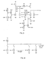
- FIG. 1 there is shown the relationship of a number of known circuit elements within the memory of the invention. While each of the identified sub-elements are well known and thus require no detailed description of operation, their specific relationship to each other is unique and requires explanation. Proceeding from left to right the following functional elements are provided:
- the circuit is precharged by WSARP (the drive phase for the address true/complement generator) and triggered when one of the word true and complement signals SAR2T and SAR2C, are applied to the conduction electrodes of T37 and T45 respectively, have risen enough to discharge a simulated word decode NOR node at the drain of T38 and T41.
- the WLP phase drives one of two first level word lines VW1 or VW2, which are used in turn to drive the reference word lines through the word and reference word decoders.
- the word drive clock or phase is generated unconditionally after the application of row address signals to the memory, assuming the memory has in fact been selected.
- the voltage designation VDM is an alternative designation for the drain supply voltage Vdd.
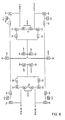
- FIG. 3. shows one of two nearly identical circuits used to generate the first level decode signal in response to word address input SAR1.
- the circuit show generates the phase VW1 signal in response to the input SAR1T while the circuit not shown generates the signal VW2 in response to the input SAR1C.
- the circuit is precharged by phase WDRP charging the gate of T7 high during standby time.
- the word address signals have been generated if the word address SARx coupled to the conductive electrode of T10 remains low, then when the word drive phase WLP rises the output VWx will follow. If the input SARx rises device 9 and 4 will both conduct discharging both the precharged gate of device 7 and the output. Of particular significance is the presence of the input signal VWKILL.
- VWKILL represents a means to disable the word drive signal from propagating to the word line driver circuit as will be shown below.
- FIG. 4 shows the redundant decoder circuit which is a simple NOR decoder in which there have been placed fuses to enable the circuit to respond to any address combination desired.
- FIG. 5 shows the wordline decoder circuits of standard design. These circuits, of which there as many as there are wordlines in the memory, are responsive to the applied true and complement (T/C) address signals to couple which ever one of VW1 and VW2 which have been generated by the first level decoder.
- T/C true and complement
- FIG. 6 shows the reference wordline decoder which in response to both the phase VW1 or VW2 and the row address SAR2 (designated WS2T/C) generates the proper reference wordline signal to select a reference cell for the cells in the normal array. Recall that during selection of a redundant wordline, the output VWx is inhibited, and thus that of the reference wordline circuit as well.
- FIG. 7 show the most significant circuit of the invention, that of the VWKILL circuit.
- the VWKILL circuit is responsive to the signals generated by the redundant wordline decoder NOR circuits as designated by the inputs RNOR1-RNOR4.
- the redundant decoder outputs are coupled in pairs to the inputs of ENOR circuits formed by the cross-coupled devices 1 and 2 and 3 and 4, the outputs of which are commonly coupled to the gate of device 9.
- the output of the ENOR gates is precharged to the same Vdd-Vt as that of the RNOR circuits so that initially all of devices 1-4 are non-conductive.
- the deselected redundant NOR nodes will discharge at different rates dependent upon the number of NOR devices pulling it low. Therefore, from redundant NOR node to redundant NOR node, skews in fall time will occur as determined by the memory address and the programmed address of the redundant decoders. These variations can cause any of the EXOR devices to momentarily conduct, if this occurs between inputs of the same EXOR subcircuit and causes the voltage difference to exceed a device threshold. If the conduction is sufficient, the voltage on the gate of device 9 can be momentarily caused to droop allowing the voltage on the drain glitch positively when it is intended to remain low (unselected).
- the filter stage is used to filter this potential glitch to an insignificant level.
- the filter works by using the redundant NOR nodes to enable pass devices 10, 12, 14 and 16 (one for each NOR node) which are connected in parallel and inserted between the drain of device 9 and the final output, VWKILL.
- pass devices 10, 12, 14 and 16 one for each NOR node
- VWKILL the final output
- the usefulness of the VWKILL signal is that it is generated in between the driving of the word addresses on the internal chip address bus and the firing of the wordline clock driver.
- the VW decoders (FIG. 3) have been disabled to block the drive signal from the normal array word decoders. In this way, redundant wordlines are invoked without any added delay to the access path and without allowing any leakage of the wordline drive phase to the array word decoders.
- the circuit of this invention represents an advancement in the implementation of word redundancy in DRAM designs. Redundant address detection and subsequent wordline drive steering are accomplished without adding any delay to the access path. Circuit area and power requirements are in keeping with the efficiencies demanded of cost/performance custom memories.
- circuit technique(s) described are extendable to a broad range of technologies (CMOS, bipolar, and GaAs) and designs (Display RAM's, SRAM's, etc.) and will be useful in maintaining a performance lead in the highly competitive area of memory design.
Landscapes
- For Increasing The Reliability Of Semiconductor Memories (AREA)
- Dram (AREA)
- Techniques For Improving Reliability Of Storages (AREA)
- Static Random-Access Memory (AREA)
Applications Claiming Priority (2)
| Application Number | Priority Date | Filing Date | Title |
|---|---|---|---|
| US07/175,883 US5022006A (en) | 1988-04-01 | 1988-04-01 | Semiconductor memory having bit lines with isolation circuits connected between redundant and normal memory cells |
| US175883 | 1988-04-01 |
Publications (3)
| Publication Number | Publication Date |
|---|---|
| EP0335149A2 true EP0335149A2 (fr) | 1989-10-04 |
| EP0335149A3 EP0335149A3 (fr) | 1991-03-20 |
| EP0335149B1 EP0335149B1 (fr) | 1995-08-16 |
Family
ID=22642051
Family Applications (1)
| Application Number | Title | Priority Date | Filing Date |
|---|---|---|---|
| EP89104168A Expired - Lifetime EP0335149B1 (fr) | 1988-04-01 | 1989-03-09 | Agencement de redondance de mémoire à semi-conducteur |
Country Status (4)
| Country | Link |
|---|---|
| US (1) | US5022006A (fr) |
| EP (1) | EP0335149B1 (fr) |
| JP (1) | JPH0756758B2 (fr) |
| DE (1) | DE68923811T2 (fr) |
Cited By (7)
| Publication number | Priority date | Publication date | Assignee | Title |
|---|---|---|---|---|
| EP0435287A1 (fr) * | 1989-12-25 | 1991-07-03 | Nec Corporation | Dispositif de mémoire à semi-conducteurs |
| EP0470394A1 (fr) * | 1990-07-13 | 1992-02-12 | Sony Corporation | Dispositif de mémoire à semiconducteur avec amplificateur pour la conversion courant-tension |
| FR2670943A1 (fr) * | 1990-12-22 | 1992-06-26 | Samsung Electronics Co Ltd | Moyen de redondance d'un dispositif de memoire a semiconducteurs et procede s'y rapportant. |
| EP0579366A3 (en) * | 1992-07-13 | 1996-06-26 | Samsung Electronics Co Ltd | Redundancy circuits for semiconductor memory devices |
| US6058052A (en) * | 1997-08-21 | 2000-05-02 | Cypress Semiconductor Corp. | Redundancy scheme providing improvements in redundant circuit access time and integrated circuit layout area |
| EP1150211A2 (fr) | 2000-04-27 | 2001-10-31 | STMicroelectronics, Inc. | Mémoire de redondance pour mémoires dynamiques à accès aléatoire avec architecture de lignes de bits croisées |
| DE102004054968A1 (de) * | 2004-11-13 | 2006-05-24 | Infineon Technologies Ag | Verfahren zum Reparieren und zum Betreiben eines Speicherbauelements |
Families Citing this family (11)
| Publication number | Priority date | Publication date | Assignee | Title |
|---|---|---|---|---|
| US5629907A (en) * | 1991-06-18 | 1997-05-13 | Dallas Semiconductor Corporation | Low power timekeeping system |
| US5134616A (en) * | 1990-02-13 | 1992-07-28 | International Business Machines Corporation | Dynamic ram with on-chip ecc and optimized bit and word redundancy |
| GB9023867D0 (en) * | 1990-11-02 | 1990-12-12 | Mv Ltd | Improvements relating to a fault tolerant storage system |
| JPH04255998A (ja) * | 1991-02-08 | 1992-09-10 | Nec Ic Microcomput Syst Ltd | 半導体記憶装置 |
| US6263400B1 (en) * | 1997-08-21 | 2001-07-17 | Altera Corporation | Memory cells configurable as CAM or RAM in programmable logic devices |
| JP2000298997A (ja) * | 1999-04-15 | 2000-10-24 | Nec Corp | 半導体メモリ装置、データ設定方法および装置、情報記憶媒体 |
| DE19956069A1 (de) * | 1999-11-22 | 2001-05-31 | Infineon Technologies Ag | Integrierter Speicher mit Speicherzellen und Referenzzellen |
| JP4050690B2 (ja) * | 2003-11-21 | 2008-02-20 | 株式会社東芝 | 半導体集積回路装置 |
| KR100557712B1 (ko) * | 2004-11-10 | 2006-03-07 | 삼성전자주식회사 | 반도체 메모리의 리페어 방법 및 장치 |
| US7224626B2 (en) * | 2005-04-18 | 2007-05-29 | Infineon Technologies Ag | Redundancy circuits for semiconductor memory |
| JP4952137B2 (ja) * | 2006-08-17 | 2012-06-13 | 富士通セミコンダクター株式会社 | 半導体メモリおよびシステム |
Family Cites Families (12)
| Publication number | Priority date | Publication date | Assignee | Title |
|---|---|---|---|---|
| JPS563499A (en) * | 1979-06-25 | 1981-01-14 | Fujitsu Ltd | Semiconductor memory device |
| JPS5928560Y2 (ja) * | 1979-11-13 | 1984-08-17 | 富士通株式会社 | 冗長ビットを有する記憶装置 |
| US4389715A (en) * | 1980-10-06 | 1983-06-21 | Inmos Corporation | Redundancy scheme for a dynamic RAM |
| DE3101802A1 (de) * | 1981-01-21 | 1982-08-19 | Siemens AG, 1000 Berlin und 8000 München | Monolithisch integrierter halbleiterspeicher |
| JPS58130495A (ja) * | 1982-01-29 | 1983-08-03 | Toshiba Corp | 半導体記憶装置 |
| JPS59203299A (ja) * | 1983-05-06 | 1984-11-17 | Nec Corp | 冗長ビット付メモリ |
| JPS6031038A (ja) * | 1983-07-29 | 1985-02-16 | Shimadzu Corp | 構造物試験機 |
| JPH0666394B2 (ja) * | 1983-12-16 | 1994-08-24 | 富士通株式会社 | 半導体記憶装置 |
| JPS60145600A (ja) * | 1984-01-09 | 1985-08-01 | Nec Corp | 冗長ビツトを備えた半導体メモリ |
| DE3477973D1 (en) * | 1984-08-02 | 1989-06-01 | Siemens Ag | Integrated write-read memory |
| JPS62222500A (ja) * | 1986-03-20 | 1987-09-30 | Fujitsu Ltd | 半導体記憶装置 |
| JP2577724B2 (ja) * | 1986-07-31 | 1997-02-05 | 三菱電機株式会社 | 半導体記憶装置 |
-
1988
- 1988-04-01 US US07/175,883 patent/US5022006A/en not_active Expired - Fee Related
-
1989
- 1989-03-09 EP EP89104168A patent/EP0335149B1/fr not_active Expired - Lifetime
- 1989-03-09 DE DE68923811T patent/DE68923811T2/de not_active Expired - Lifetime
- 1989-03-09 JP JP1055261A patent/JPH0756758B2/ja not_active Expired - Lifetime
Cited By (12)
| Publication number | Priority date | Publication date | Assignee | Title |
|---|---|---|---|---|
| EP0435287A1 (fr) * | 1989-12-25 | 1991-07-03 | Nec Corporation | Dispositif de mémoire à semi-conducteurs |
| EP0470394A1 (fr) * | 1990-07-13 | 1992-02-12 | Sony Corporation | Dispositif de mémoire à semiconducteur avec amplificateur pour la conversion courant-tension |
| US5388078A (en) * | 1990-07-13 | 1995-02-07 | Sony Corporation | Semiconductor memory device having current to voltage conversion type amplifier |
| FR2670943A1 (fr) * | 1990-12-22 | 1992-06-26 | Samsung Electronics Co Ltd | Moyen de redondance d'un dispositif de memoire a semiconducteurs et procede s'y rapportant. |
| EP0579366A3 (en) * | 1992-07-13 | 1996-06-26 | Samsung Electronics Co Ltd | Redundancy circuits for semiconductor memory devices |
| US6058052A (en) * | 1997-08-21 | 2000-05-02 | Cypress Semiconductor Corp. | Redundancy scheme providing improvements in redundant circuit access time and integrated circuit layout area |
| EP1150211A2 (fr) | 2000-04-27 | 2001-10-31 | STMicroelectronics, Inc. | Mémoire de redondance pour mémoires dynamiques à accès aléatoire avec architecture de lignes de bits croisées |
| JP2001357695A (ja) * | 2000-04-27 | 2001-12-26 | Stmicroelectronics Inc | ツイスト型ビット線アーキテクチャを有するダイナミックランダムアクセスメモリ用冗長メモリセル |
| EP1150211A3 (fr) * | 2000-04-27 | 2004-09-01 | STMicroelectronics, Inc. | Mémoire de redondance pour mémoires dynamiques à accès aléatoire avec architecture de lignes de bits croisées |
| DE102004054968A1 (de) * | 2004-11-13 | 2006-05-24 | Infineon Technologies Ag | Verfahren zum Reparieren und zum Betreiben eines Speicherbauelements |
| DE102004054968B4 (de) * | 2004-11-13 | 2006-11-02 | Infineon Technologies Ag | Verfahren zum Reparieren und zum Betreiben eines Speicherbauelements |
| US7372749B2 (en) | 2004-11-13 | 2008-05-13 | Infineon Technologies Ag | Methods for repairing and for operating a memory component |
Also Published As
| Publication number | Publication date |
|---|---|
| EP0335149B1 (fr) | 1995-08-16 |
| US5022006A (en) | 1991-06-04 |
| EP0335149A3 (fr) | 1991-03-20 |
| JPH0212699A (ja) | 1990-01-17 |
| JPH0756758B2 (ja) | 1995-06-14 |
| DE68923811T2 (de) | 1996-04-18 |
| DE68923811D1 (de) | 1995-09-21 |
Similar Documents
| Publication | Publication Date | Title |
|---|---|---|
| EP0335149B1 (fr) | Agencement de redondance de mémoire à semi-conducteur | |
| US5430679A (en) | Flexible redundancy architecture and fuse download scheme | |
| US5615164A (en) | Latched row decoder for a random access memory | |
| JP3129440B2 (ja) | 冗長装置を有する集積半導体メモリ | |
| EP0336101B1 (fr) | Dispositif de mémoire à semi-conducteur | |
| EP0747906B1 (fr) | Procédé de test pour une mèmoire à accès aléatoire | |
| US7274580B2 (en) | Content addressable memory device | |
| US5031151A (en) | Wordline drive inhibit circuit implementing worldline redundancy without an access time penalty | |
| US4791615A (en) | Memory with redundancy and predecoded signals | |
| JPS6337899A (ja) | 半導体記憶装置 | |
| US20110261633A1 (en) | Memory with improved data reliability | |
| EP0881571B1 (fr) | Dispositif de mémoire à semiconducteur avec rédondance | |
| HK5094A (en) | Summation of address transition signals | |
| KR100286789B1 (ko) | 메모리용 컬럼 여유도 회로 | |
| US6058052A (en) | Redundancy scheme providing improvements in redundant circuit access time and integrated circuit layout area | |
| KR920009703B1 (ko) | 메모리 회로와 행 및 열 제어 방법 | |
| US7609569B2 (en) | System and method for implementing row redundancy with reduced access time and reduced device area | |
| US5764587A (en) | Static wordline redundancy memory device | |
| US7002822B2 (en) | Content addressable memory device | |
| US6552939B1 (en) | Semiconductor memory device having disturb test circuit | |
| US6195300B1 (en) | CBR refresh control for the redundancy array | |
| US6219285B1 (en) | Semiconductor storage device with synchronized selection of normal and redundant columns | |
| US6809972B2 (en) | Circuit technique for column redundancy fuse latches | |
| US5568433A (en) | Memory array having redundant word line | |
| JP2002093188A (ja) | 半導体記憶装置 |
Legal Events
| Date | Code | Title | Description |
|---|---|---|---|
| PUAI | Public reference made under article 153(3) epc to a published international application that has entered the european phase |
Free format text: ORIGINAL CODE: 0009012 |
|
| AK | Designated contracting states |
Kind code of ref document: A2 Designated state(s): DE FR GB |
|
| 17P | Request for examination filed |
Effective date: 19900224 |
|
| PUAL | Search report despatched |
Free format text: ORIGINAL CODE: 0009013 |
|
| AK | Designated contracting states |
Kind code of ref document: A3 Designated state(s): DE FR GB |
|
| 17Q | First examination report despatched |
Effective date: 19940311 |
|
| GRAA | (expected) grant |
Free format text: ORIGINAL CODE: 0009210 |
|
| AK | Designated contracting states |
Kind code of ref document: B1 Designated state(s): DE FR GB |
|
| REF | Corresponds to: |
Ref document number: 68923811 Country of ref document: DE Date of ref document: 19950921 |
|
| ET | Fr: translation filed | ||
| PGFP | Annual fee paid to national office [announced via postgrant information from national office to epo] |
Ref country code: FR Payment date: 19960307 Year of fee payment: 8 |
|
| PG25 | Lapsed in a contracting state [announced via postgrant information from national office to epo] |
Ref country code: GB Effective date: 19960309 |
|
| PLBE | No opposition filed within time limit |
Free format text: ORIGINAL CODE: 0009261 |
|
| STAA | Information on the status of an ep patent application or granted ep patent |
Free format text: STATUS: NO OPPOSITION FILED WITHIN TIME LIMIT |
|
| 26N | No opposition filed | ||
| GBPC | Gb: european patent ceased through non-payment of renewal fee |
Effective date: 19960309 |
|
| PGFP | Annual fee paid to national office [announced via postgrant information from national office to epo] |
Ref country code: DE Payment date: 19970326 Year of fee payment: 9 |
|
| PG25 | Lapsed in a contracting state [announced via postgrant information from national office to epo] |
Ref country code: FR Free format text: LAPSE BECAUSE OF NON-PAYMENT OF DUE FEES Effective date: 19971128 |
|
| REG | Reference to a national code |
Ref country code: FR Ref legal event code: ST |
|
| PG25 | Lapsed in a contracting state [announced via postgrant information from national office to epo] |
Ref country code: DE Free format text: LAPSE BECAUSE OF THE APPLICANT RENOUNCES Effective date: 19980323 |