EP0335217A2 - Diode schottky intégrée avec un transistor - Google Patents
Diode schottky intégrée avec un transistor Download PDFInfo
- Publication number
- EP0335217A2 EP0335217A2 EP89104969A EP89104969A EP0335217A2 EP 0335217 A2 EP0335217 A2 EP 0335217A2 EP 89104969 A EP89104969 A EP 89104969A EP 89104969 A EP89104969 A EP 89104969A EP 0335217 A2 EP0335217 A2 EP 0335217A2
- Authority
- EP
- European Patent Office
- Prior art keywords
- region
- type
- providing
- depth
- substrate
- Prior art date
- Legal status (The legal status is an assumption and is not a legal conclusion. Google has not performed a legal analysis and makes no representation as to the accuracy of the status listed.)
- Withdrawn
Links
Images

Classifications
-
- H—ELECTRICITY
- H10—SEMICONDUCTOR DEVICES; ELECTRIC SOLID-STATE DEVICES NOT OTHERWISE PROVIDED FOR
- H10D—INORGANIC ELECTRIC SEMICONDUCTOR DEVICES
- H10D84/00—Integrated devices formed in or on semiconductor substrates that comprise only semiconducting layers, e.g. on Si wafers or on GaAs-on-Si wafers
- H10D84/01—Manufacture or treatment
- H10D84/0107—Integrating at least one component covered by H10D12/00 or H10D30/00 with at least one component covered by H10D8/00, H10D10/00 or H10D18/00, e.g. integrating IGFETs with BJTs
- H10D84/0109—Integrating at least one component covered by H10D12/00 or H10D30/00 with at least one component covered by H10D8/00, H10D10/00 or H10D18/00, e.g. integrating IGFETs with BJTs the at least one component covered by H10D12/00 or H10D30/00 being a MOS device
-
- H—ELECTRICITY
- H03—ELECTRONIC CIRCUITRY
- H03K—PULSE TECHNIQUE
- H03K17/00—Electronic switching or gating, i.e. not by contact-making and –breaking
- H03K17/06—Modifications for ensuring a fully conducting state
-
- H—ELECTRICITY
- H03—ELECTRONIC CIRCUITRY
- H03K—PULSE TECHNIQUE
- H03K17/00—Electronic switching or gating, i.e. not by contact-making and –breaking
- H03K17/06—Modifications for ensuring a fully conducting state
- H03K17/063—Modifications for ensuring a fully conducting state in field-effect transistor switches
-
- H—ELECTRICITY
- H10—SEMICONDUCTOR DEVICES; ELECTRIC SOLID-STATE DEVICES NOT OTHERWISE PROVIDED FOR
- H10D—INORGANIC ELECTRIC SEMICONDUCTOR DEVICES
- H10D8/00—Diodes
- H10D8/01—Manufacture or treatment
- H10D8/051—Manufacture or treatment of Schottky diodes
-
- H—ELECTRICITY
- H10—SEMICONDUCTOR DEVICES; ELECTRIC SOLID-STATE DEVICES NOT OTHERWISE PROVIDED FOR
- H10D—INORGANIC ELECTRIC SEMICONDUCTOR DEVICES
- H10D8/00—Diodes
- H10D8/60—Schottky-barrier diodes
-
- H—ELECTRICITY
- H10—SEMICONDUCTOR DEVICES; ELECTRIC SOLID-STATE DEVICES NOT OTHERWISE PROVIDED FOR
- H10D—INORGANIC ELECTRIC SEMICONDUCTOR DEVICES
- H10D84/00—Integrated devices formed in or on semiconductor substrates that comprise only semiconducting layers, e.g. on Si wafers or on GaAs-on-Si wafers
- H10D84/01—Manufacture or treatment
- H10D84/0112—Integrating together multiple components covered by H10D8/00, H10D10/00 or H10D18/00, e.g. integrating multiple BJTs
-
- H—ELECTRICITY
- H10—SEMICONDUCTOR DEVICES; ELECTRIC SOLID-STATE DEVICES NOT OTHERWISE PROVIDED FOR
- H10D—INORGANIC ELECTRIC SEMICONDUCTOR DEVICES
- H10D84/00—Integrated devices formed in or on semiconductor substrates that comprise only semiconducting layers, e.g. on Si wafers or on GaAs-on-Si wafers
- H10D84/01—Manufacture or treatment
- H10D84/02—Manufacture or treatment characterised by using material-based technologies
- H10D84/03—Manufacture or treatment characterised by using material-based technologies using Group IV technology, e.g. silicon technology or silicon-carbide [SiC] technology
- H10D84/038—Manufacture or treatment characterised by using material-based technologies using Group IV technology, e.g. silicon technology or silicon-carbide [SiC] technology using silicon technology, e.g. SiGe
-
- H—ELECTRICITY
- H10—SEMICONDUCTOR DEVICES; ELECTRIC SOLID-STATE DEVICES NOT OTHERWISE PROVIDED FOR
- H10D—INORGANIC ELECTRIC SEMICONDUCTOR DEVICES
- H10D84/00—Integrated devices formed in or on semiconductor substrates that comprise only semiconducting layers, e.g. on Si wafers or on GaAs-on-Si wafers
- H10D84/60—Integrated devices formed in or on semiconductor substrates that comprise only semiconducting layers, e.g. on Si wafers or on GaAs-on-Si wafers characterised by the integration of at least one component covered by groups H10D10/00 or H10D18/00, e.g. integration of BJTs
- H10D84/611—Combinations of BJTs and one or more of diodes, resistors or capacitors
- H10D84/613—Combinations of vertical BJTs and one or more of diodes, resistors or capacitors
- H10D84/617—Combinations of vertical BJTs and only diodes
-
- H—ELECTRICITY
- H10—SEMICONDUCTOR DEVICES; ELECTRIC SOLID-STATE DEVICES NOT OTHERWISE PROVIDED FOR
- H10D—INORGANIC ELECTRIC SEMICONDUCTOR DEVICES
- H10D62/00—Semiconductor bodies, or regions thereof, of devices having potential barriers
- H10D62/80—Semiconductor bodies, or regions thereof, of devices having potential barriers characterised by the materials
- H10D62/85—Semiconductor bodies, or regions thereof, of devices having potential barriers characterised by the materials being Group III-V materials, e.g. GaAs
Definitions
- This invention relates to means and methods for forming improved transistors and Schottky diodes and more particularly, to means and methods for forming integrated Schottky diodes and transistors.
- a charge pump that is, a means for providing internally a voltage which is above the supply voltage or not readily derived from the supply voltage by the usual voltage dividers.
- this has been accomplished by using a transistor connected as a diode in a voltage doubler circuit.
- this approach suffers from a number of limitations well known in the art. It has been found that improved devices may be prepared by using an integrated Schottky diode for this function.
- a Schottky diode may also be used in smart-power devices as a clamp diode or charge pump rectifier or as an improved Kelvin voltage sense contact to the collector region of a bipolar transistor to provide improved clamping of the emitter-base voltage.
- a semiconductor device having an integrated Schottky diode comprising: a semiconductor substrate having a major surface and containing a first region of a first type extending to the surface and having a first depth into the substrate; a second region of a second type opposite the first type, located within the first region, extending to the surface and having a second depth into the substrate; a third region of the first type, located within the second region, extending to the surface and having a third depth into the substrate; optionally, a fourth region of the second type located within the third region, extending to the surface and having, a fourth depth into the substrate; a fifth region of the second type located within the third region, extending to the surface, at least partially overlapping the fourth region and having a fifth depth into the substrate less than the third depth; a first portion of the surface including a first part of the third region at the surface and a first part of the fourth region at the surface; and a conductor on the first portion of the surface wherein the conductor forms an
- the Schottky diode incorporates a Kelvin probe contact to the collector region of a bipolar transistor
- the fourth region be deeper than the third region and, when viewed looking toward the surface, have U-shaped arms substantially enclosing the fifth region on three sides leaving a fourth side of the fifth region not enclosed by the fourth region.
- the fifth region desirably has an annular shape with the Schottky contact to the third region located in the center thereof. It is further desirable that the device comprise a sixth region of the second type located within the third region, separated from the fourth side of the fifth region by another part of the third region, extending to the surface and having a depth into the substrate less than the third depth.
- Optional seventh and eighth doped regions are desirably located at the surface, respectively, at an intersection of the second and third regions and at an intersection of the second and first regions, wherein the seventh region is of the first type and has a depth into the substrate less than the third region and the eighth region is of the second type and has a depth less than the second region.
- An integrated Schottky diode structure is conveniently formed by the steps of: providing a semiconductor substrate having a first region of a first type extending to a principal surface; providing a second doped region of a second type opposite the first type which forms a first junction with the first region extending to the surface; providing a third doped region of the first type in the second region which forms a second junction with the second region extending to the surface; then in either order, (a) providing a fourth doped region of the second type located at the intersection of the first junction and the surface and a fifth doped region of the second type laterally within the third region at the surface, and (b) providing a sixth doped region of the first type located at the intersection of the second junction and the surface; exposing first, second and third portions of the surface, respectively, on the fourth, fifth, and sixth doped regions and a fourth portion of the surface laterally within the third region desirably adjacent to the second portion of the surface; and providing a Schottky contact to the fourth portion of the surface which extends onto
- Further contact is desirably provided by covering the conductor used for the Schottky contact with a diffusion barrier conductor and then covering the diffusion barrier conductor with a further conductor.
- the impurity concentration at the surface of the second portion exceeds 1019 atoms/cm3, preferably exceeding about 1020 atoms/cm3, and that the impurity concentration at the surface of the fourth portion is less than 1018 atoms/cm3, preferably less than about 1017 atoms/cm3.
- the Schottky contact be substantially laterally surrounded by a doped region of the second type located in the third region and having a depth less than the third region.
- the fifth region be U shaped when viewed perpendicular to the substrate surface and extend through the third region and surround on three sides a further region of the same type located in and not extending through the third region, and that there be provided a still further region of the same type in and shallower than the third region and laterally spaced from the further region.
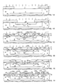
- FIGS. 1A-1F show simplified cross-sections of a portion of a semiconductor chip of, for example silicon, containing a smart-power device with an integrated Schottky, during different stages of fabrication.
- the semiconductor chips are first prepared in the form of wafers containing many identical chips which are then cut apart to yield the final smart-power device. Many individual devices may be provided on a single smart-power chip.
- dielectric mask layer 2 e.g., silicon oxide or silicon nitride or silicon oxynitride or the like
- photoresist mask layer 3 are provided on surface 4 of substrate 5.
- Substrate 5 of, for example N+ silicon has therein doped region 6 (e.g., N-), which is conveniently formed, for example, by epitaxial growth although other methods for forming region 6 may also be used.
- region 6 is heavily doped and region 6 is typically lightly doped, for example to about 3x10¹⁵ /cm3, but other doping levels in the range 1014 to 5x10¹⁶ /cm3 may also be used.
- doping level of region 6 depending upon the desired final device characteristics.
- Opening 7 is provided extending through layers 2, 3 to surface 4 using means well known in the art.
- Lightly doped (e.g., P-) region 8 of opposite type to region 6 is formed typically by ion implantation of impurity 9 through mask opening 7 followed by annealing and activation.
- Preferred implant conditions are about 90 keV and 5x10¹² ions/cm2 (boron) followed by a thermal anneal at about 1200 °C for times up to about 15 hours, followed by a second implant at about the same energy (but through a thicker surface oxide) and a higher dose, e.g., about 1.3x10¹³ ions/cm2, to locate the peak of the second implant at a shallower depth than the first implant and with a higher concentration.
- the second implant is conveniently annealed during subsequent thermal process steps and while a separate annealing step may be used it is not necessary.
- the use of a double implant allows the dopant profile to be more closely adjusted and is a desirable feature of the present process.
- the resulting boron surface concentration of region 8 after annealing is determined primarily by the second implant and is about 2x10¹⁶ /cm3, but surface concentrations in the range 5x10¹⁵ to 5x10¹⁶ /cm3 are also useful.
- the first implant and long anneal produces a dopant tail extending deeply into the substrate.
- region 8 While ion implantation is preferred for forming region 8, other methods may also be used. It is desirable that region 8 be shallower than region 6 so as to not extend into substrate 5. This provides higher breakdown and lower leakage between region 8 and substrate 5. Dielectric is conveniently reformed in window 7 during or after drive-in of dopant 9 so as to provide dielectric 10 covering surface 4 for the next masking step.
- substrate 5 containing doped regions 6 and 8 has dielectric layer 10 and photomask layer 11 on surface 4.
- Layers 10 and 11 are etched using means well known in the art to provide opening 12 extending to surface 4.
- Impurity 13 is provided, again conveniently by ion implantation, to form lightly doped region 14 (e.g., N-) of opposite type than region 8, located within region 8 and extending to surface 4.
- lightly doped region 14 e.g., N-
- Typical conditions are a dose of about 1x10¹³ ions/cm2 (phosphorous) at about 120 keV although other energies and doses may be used.
- Annealing is typically performed at about 1150°C for about two hours.
- Surface phosphorous concentrations in region 14 are typically about 6x10¹⁶ /cm3 after annealing.
- region 14 It is important that the surface impurity concentration of region 14 be equal to or higher than that of region 8 so that the semiconductor surface has the conductivity type associated with the dopant of region 14. Region 14 is not as deep as region 8 so that an undisturbed portion of region 8 remains between region 14 and region 6. The junction between regions 8 and 14 is desirably located in the dopant tail region determined primarily by the first (lower dose, long anneal time) boron implant.
- Dielectric is conveniently re-formed in opening 12 using means well known in the art so as to provide dielectric 15 for the next masking step (see FIG. 1C).
- Dielectric 15, which may consist for example of silicon oxide, nitride or combinations thereof, is etched using means well known in the art (not shown) to provide openings 15A-F therein extending to surface 4. Openings 15A-F act as master-mask openings for the remainder of the fabrication steps and, since they are formed at the same time, are self-aligned. Master-masking techniques are described for example in U. S. Patents 4,199,380 and RE 30,282 which are incorporated herein by reference.
- Portion 15G (shown dashed in FIG. 1C) of layer 15 may be left in place above portion 22 of surface 4 or removed as a part of the formation of master mask 15. It is more convenient to remove portion 15G since, as will be subsequently explained, this avoids a later masking step.
- block-out mask 16 of, for example photoresist is applied over master-mask 15. Openings 16A-C of mask 16 are oversized so as to avoid critical alignment requirements. Openings 16A-C select openings 15A, 15C, 15D and 15F of master-mask 15 so that impurities 17 may be implanted or otherwise introduced into substrate 10 in locations 26, 28, 29, and 30. Where portion 15G has been omitted, then portion 16D of mask 16 is included to cover portion 22 of surface 4 between doped regions 28, 29. Where portion 15G has been included then portion 16D may be omitted since portion 15G covers portion 22 between 28, 29.
- Boron is a suitable dopant where these regions are desired to be P-type and a heavy dose (e.g., about 1015 /cm2 at about 40-50 keV) is desirable so as to make these regions heavily doped, e.g., P+.
- Activation and annealing may be performed anytime after implantation of impurity 17, e.g., before or after the step shown in FIG. 1D.
- block-out mask 18 having oversized openings 18A-B is applied over master-mask 15 so as to select openings 15B and 15E through which impurities 19 (e.g., phosphorous) are introduced to form heavily doped (e.g., N+) regions 34, 36, respectively.
- impurities 19 e.g., phosphorous
- Doped regions 26-36 are conveniently annealed and activated together, providing the result shown in FIG. 1E. While ion implantation is preferred for forming doped regions 26-36, it is not essential and any means for introducing a comparatively high concentration (e.g., N+ or P+) impurity into these regions may be used. Such means are well known in the art. Further, the steps illustrated in FIGS. 1C and 1D may be interchanged in order.
- the step shown in FIG. 1E is only needed where portion 15G of mask 15 has been left in place.
- Mask 20 having opening 21 is provided to select portion 22 of surface 4 of substrate 10 lying between regions 28, 29. Opening 21 is oversized to avoid critical alignment. Opening 21 must overlap at least one and preferably both of openings 15C and 15D of master mask 15 so that when portion 15G of mask 15 overlying surface portion 22 is removed, part of one or both of 28 and 29 are also exposed. Mask 20 is then removed.
- portion 15G is not provided then the step of FIG. 1E is not needed. This is preferable since it avoids a masking step, but either procedure produces satisfactory results.
- openings 15C-D when viewed looking at the plane of surface 4, join so as to form a closed, annular shaped opening surrounding portion 22 of surface 4. If the Schottky contact is not surrounded at the surface by a contiguous PN junction then leakage is increased. Openings 15B, 15E and 15A, 15F may likewise join to form closed annular shapes in the plane of the substrate surface. This is desirable but not essential.
- Conductor 23 applied to the structure so as to make contact with the portions of surface 4 exposed in openings 15A-15F and with portion 22 (see FIG. 1F).
- the material of conductor 23 must be chosen so as to make a Schottky contact to surface portion 22 of semiconductor substrate 5 and ohmic contact to regions 28, 29. It is also desirable that the contacts between conductor 23 and the portions of surface 4 exposed in openings 15A, 15B, 15E and 15F also be ohmic.
- Conductor 23 is desirably formed from two or more layers, e.g., layers 23A-C.
- Layer 23A must have the above described contacting properties, i.e., form a Schottky barrier on surface portion 22 of region 14 and ohmic contact to highly doped regions 26-36.
- Layer 23B is provided to prevent solid-solid interdiffusion of layer 23A and to provide more conductive and more easily bonded overlayer 23C.
- Schottky contacts Semiconductor-metal combinations suitable for forming Schottky contacts are well known in the art. For example, where a Schottky contact is desired to N- silicon, platinum or platinum silicide is suitable for layer 23A, Ti-W is suitable for layer 23B, and AlSi or AlCu or AlSiCu is suitable for layer 23C. Other metals and intermetallics well known in the art may also be used for the Schottky contact. Layer 23B conveniently acts as a barrier material to prevent interaction of layers 23A and 23C. However, other conductive material combinations can also be used. Those of skill in the art will understand how to choose appropriate material combinations based on the description given herein and deposit them on substrate 10. Such materials and methods are known in the art.
- Contacts 24A, 24E are desirably part of the same annular ohmic contact to P+ regions 26, 30 which provide contact to P- region 8.
- Contacts 24B, 24D are desirably part of the same annular ohmic contact to N+ regions 34, 36 which provide contact to N- region 14.
- P+ regions 28, 29 act as a guard ring for Schottky contact 24C to surface portion 22 of region 14.
- contacts 24A, 24E; 24B, 24D; and 24C may extend to other devices (not shown) so as to interconnect the Schottky diode formed between contacts 24C and contacts 24B, 24D as is required by the circuit function (e.g., see FIG. 5).
- FIGS. 2A-2F are similar to FIGS. 1A-1F, but illustrate a further embodiment of the invention.
- the same numbers are used to identify device regions formed in substantially the same locations and by the same procedures and having substantially similar functions.
- FIGS. 2A-2F show cross-sections along the center-line of FIG. 3 during different stages of fabrication.
- N+ substrate 5 having N-region 6 and P- region 8 is provided as has already been described in connection with FIGS. 1A-F.
- Surface 4 of substrate 5 is covered by dielectric 35 and mask 37 in which openings 35A-C have been opened to surface 4 to allow, respectively, formation of moderately doped (e.g., P), regions 40, 41, 42 of the same type as region 8 by implantation and diffusion of impurity 38.
- moderately doped e.g., P
- regions 40, 41, 42 of the same type as region 8 by implantation and diffusion of impurity 38.
- Regions 40-42 may be formed by doping means other than ion implantation.
- the depth of region 41 in relation to the depth of region 14 is important.
- the depths of regions 40 and 42 are not critical and they are formed at the same time as region 41 merely for convenience. Regions 40, 42 are preferred but may be omitted.
- the dielectric removed in openings 37A-C is conveniently replaced to form dielectric 44 for the next masking step illustrated in FIG. 2B.
- Mask 11 is applied in the same manner as in FIG. 1B and region 14 formed in region 8 in the same way as previously described.
- the order of the steps illustrated in FIGS. 2A and 2B may be interchanged with respect to forming regions 40-42 and 14.
- master mask 45 analogous to master-mask 15 is applied having openings 45A-G extending to surface 4.
- Portion 45H of mask 45 above surface portion 62 of surface 4 may be provided or omitted in a manner analogous to portions 15G of mask 15 in FIG. 1C.
- portion 45H is shown dashed in FIG. 2c. In the preferred embodiment it is omitted.
- Block-out mask 46 having openings 46A-C is applied (FIG. 2c) to select openings 45A, 45C, 45D, 45E, and 45G so that impurities 47 may be implanted to form, respectively, highly doped (e.g., P+) regions 26-30 in surface 4 of substrate 5.
- P+ regions 26-30 in surface 4 of substrate 5.
- two other P+ regions 27, 28 also lie within N-region 14 but are spaced apart from P+ region 29.
- closed portion 46D is provided to separate regions 28, 29 in a manner analogous to region 16D in FIG. 1C.
- regions 28, 29 are desirably part of a common annular shaped P+ region with central opening 62.
- FIG. 2D further block-out mask 48 is provided having openings 48A-B which select openings 45B, 45F, respectively, in master-mask 45.
- Mask 48 is analogous to mask 18 of FIG. 1D.
- Dopant 49 is provided through openings 48A-B to form highly doped regions 34, 36, (e.g., N+) respectively in surface 4 of substrate 5, in the same manner as has been previously described.
- the order of the steps illustrated in FIGS. 2c, 2D may be interchanged, just as with the order of the steps in FIGS. 1C, 1D, and the activation/annealing of the implants may be performed individually or simultaneously, as has been previously described. The result is shown in FIG. 2E.
- FIG. 2E The step of FIG. 2E is only needed where portion 45H of mask 45 has been left in place, as shown by the dashed line in FIGS. 2C-D. It is conveniently removed here using block-out mask 50 so as to expose portion 62 of surface 4 located between regions 28, 29. Opening 51 corresponds to opening 21 of FIG. 1E and exposed surface portion 62 is analogous to portion 22. Mask 50 is then removed.
- contacts 54A-C and 54E analogous to contacts 24A-C and 24E, respectively.
- Additional contact 54G is also formed to region 27 in FIG. 2F.
- a contact analogous to contact 24D may be provided tc region 36 but is not necessary and has been omitted from FIG. 2F for simplicity.
- the materials and methods used to form contacts 54A-C, 54E and 54G are the same as used for forming 24A-D.
- FIG. 3 provides a top and partial cut-away view of the structure of FIGS. 2A-2F, that is, looking at the plane of surface 4, with the various masks used to form the device superimposed and looking at the cross-section along centerline 90 with the resulting doped regions outlined.
- the device of FIG. 3 is desirably symmetrical about centerline 90.
- Outline 70 indicates the relative location of mask opening 7 used to form P- tub 8.
- Outline 72 indicates the relative location of mask opening 12 used to form N-region 14.
- Outlines 74 indicates the relative location of openings 37A, 37C and outline 76 indicates the relative location of opening 37B.
- Outlines 78 indicate the relative locations of openings 45A, 45C, 45D, 45E, and 45G through which P+ regions 26-30 are formed and outlines 80 indicate the relative locations of openings 45B, 45F through which N+ regions 34, 36 are formed.
- Outlines 82 are pre-ohmic masks for re-opening contact holes through dielectric 45 and outlines 84 indicate the conductive contacts.
- conductor 54a of FIG. 2F has been omitted from FIG. 3.
- the location of conductors 54B, 54C, 54E and 54G are indicated on FIG. 3. It will be apparent from FIGS.
- P+ regions 28, 29 are part of a common annular shaped P+ region with central opening 62 wherein the Schottky contact is formed, that region 41 is U-shaped and partially overlaps regions 29, and that region 28 lies between the arms of U-shaped region 41.
- FIGS. 2F and 3 It will also be apparent from FIGS. 2F and 3 that a compact integrated structure results wherein the Schottky diode is located closer to the active region of the device under emitter 27 than is collector contact diffusion 26, 30. This results in the Schottky acting as a Kelvin probe which is not affected by the series drop across internal collector resistance 97, that is the voltage drop due to the lateral current flow within region 8 to collector contact diffusion 26, 30 and collector contact 54E.
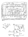
- FIG. 4 shows the equivalent circuit of the arrangement of FIGS. 2F and 3 with series collector resistance 97 indicated.
- Bipolar transistor 90 has base 92, emitter 94 and collector 96, collector series resistance 97 and Kelvin probe Schottky diode 98 connected between base and collector, but electrically ahead of collector series resistance 97.
- collector resistance is an important consideration.
- PNP devices it is frequently the case, particularly with PNP devices, that it is not practical to include a buried collector region because of conflicting process and structure requirements elsewhere in the device or where a backside collector contact is needed.
- the ability to provide a built-in Schottky Kelvin probe that is not affected by series collector resistance is an important advantage under such circumstances. This is a particular feature of the present invention.
- FIG. 5 illustrates how the Schottky diode of the present invention, as for example in FIG. 1, may be used in a charge pump circuit to provide internal circuit voltages higher than the supply voltage.
- Out of phase pulse trains 100, 102 are applied to the inputs of transistors 104, 106 which are connected between VDD and ground so that one end of capacitor 108 is alternatively switched between VDD less a threshold voltage, and ground.
- the other terminal of capacitor 108 connects to the center point of Schottky diodes 110, 112 which extend between VDD and the source of transistor 114.
- the gate of transistor 114 is connected to ground through switch 126 and the drain is connected to capacitor 116, the drain of transistor 118 and the gate of output transistor 120.
- Transistor 120 extends between VDD and load 122.
- Switches 124, 126 are used to stop and start the charge pump action.
- the action of the circuit is such that after a few cycles of the out of phase signals on transistors 104, 106, the voltage appearing on the gate of output transistor 120 exceeds the supply voltage VDD and is about twice VDD less two Schottky diode voltage drops and a threshold voltage. This substantially reduces the on-resistance of transistor 120 without having to provide a separate external power supply for the gate of transistor 120. This is a great convenience in smart-power circuits.
- a Schottky diode is available as a charge pump diode or a Kelvin sense probe for a bipolar transistor or for other purposes that will be apparent to those of skill in the art based on the description herein, in a manner not previously taught in the art, and that these advantages have been provided in a manner compatible with other processing requirements for smart-power devices.
Landscapes
- Electrodes Of Semiconductors (AREA)
- Bipolar Transistors (AREA)
- Metal-Oxide And Bipolar Metal-Oxide Semiconductor Integrated Circuits (AREA)
- Bipolar Integrated Circuits (AREA)
- Manipulation Of Pulses (AREA)
Applications Claiming Priority (2)
| Application Number | Priority Date | Filing Date | Title |
|---|---|---|---|
| US07/173,795 US4871686A (en) | 1988-03-28 | 1988-03-28 | Integrated Schottky diode and transistor |
| US173795 | 1988-03-28 |
Publications (2)
| Publication Number | Publication Date |
|---|---|
| EP0335217A2 true EP0335217A2 (fr) | 1989-10-04 |
| EP0335217A3 EP0335217A3 (fr) | 1992-04-15 |
Family
ID=22633523
Family Applications (1)
| Application Number | Title | Priority Date | Filing Date |
|---|---|---|---|
| EP19890104969 Withdrawn EP0335217A3 (fr) | 1988-03-28 | 1989-03-20 | Diode schottky intégrée avec un transistor |
Country Status (4)
| Country | Link |
|---|---|
| US (1) | US4871686A (fr) |
| EP (1) | EP0335217A3 (fr) |
| JP (1) | JPH0210765A (fr) |
| KR (1) | KR0131591B1 (fr) |
Cited By (3)
| Publication number | Priority date | Publication date | Assignee | Title |
|---|---|---|---|---|
| EP0589123A1 (fr) * | 1992-09-23 | 1994-03-30 | STMicroelectronics S.r.l. | Circuit d'attaque pour un commutateur électronique |
| EP0887933A1 (fr) * | 1997-06-24 | 1998-12-30 | STMicroelectronics S.r.l. | Circuit d'extinction pour un transistor LDMOS en présence d'un courant inverse |
| EP1211733A4 (fr) * | 1999-09-09 | 2007-01-17 | Rohm Co Ltd | Dispositif a semiconducteur |
Families Citing this family (33)
| Publication number | Priority date | Publication date | Assignee | Title |
|---|---|---|---|---|
| US5225359A (en) * | 1990-08-17 | 1993-07-06 | National Semiconductor Corporation | Method of fabricating Schottky barrier diodes and Schottky barrier diode-clamped transistors |
| US5364801A (en) * | 1990-12-17 | 1994-11-15 | Texas Instruments Incorporated | Method of forming a charge pump circuit |
| US5250834A (en) * | 1991-09-19 | 1993-10-05 | International Business Machines Corporation | Silicide interconnection with schottky barrier diode isolation |
| US5279507A (en) * | 1991-09-26 | 1994-01-18 | Yazaki Corporation | Connector for use in vehicles |
| US5268316A (en) * | 1991-12-06 | 1993-12-07 | National Semiconductor Corporation | Fabrication process for Schottky diode with localized diode well |
| US5514612A (en) * | 1993-03-03 | 1996-05-07 | California Micro Devices, Inc. | Method of making a semiconductor device with integrated RC network and schottky diode |
| US5821575A (en) * | 1996-05-20 | 1998-10-13 | Digital Equipment Corporation | Compact self-aligned body contact silicon-on-insulator transistor |
| US5763918A (en) * | 1996-10-22 | 1998-06-09 | International Business Machines Corp. | ESD structure that employs a schottky-barrier to reduce the likelihood of latch-up |
| DE10101081B4 (de) * | 2001-01-11 | 2007-06-06 | Infineon Technologies Ag | Schottky-Diode |
| FR2832547A1 (fr) * | 2001-11-21 | 2003-05-23 | St Microelectronics Sa | Procede de realisation d'une diode schottky sur substrat de carbure de silicium |
| GB0202065D0 (en) * | 2002-01-30 | 2002-03-13 | Watson Brown Hsm Ltd | Mixing |
| GB2404507B (en) * | 2003-07-31 | 2006-06-21 | Zetex Plc | A high side switching circuit |
| US6987305B2 (en) * | 2003-08-04 | 2006-01-17 | International Rectifier Corporation | Integrated FET and schottky device |
| US7696598B2 (en) * | 2005-12-27 | 2010-04-13 | Qspeed Semiconductor Inc. | Ultrafast recovery diode |
| KR100773399B1 (ko) * | 2006-10-23 | 2007-11-05 | 삼성전자주식회사 | 반도체 소자 및 그 형성 방법 |
| US7564099B2 (en) * | 2007-03-12 | 2009-07-21 | International Rectifier Corporation | Monolithic MOSFET and Schottky diode device |
| US8022446B2 (en) * | 2007-07-16 | 2011-09-20 | Taiwan Semiconductor Manufacturing Company, Ltd. | Integrated Schottky diode and power MOSFET |
| JP5530602B2 (ja) | 2008-04-09 | 2014-06-25 | ルネサスエレクトロニクス株式会社 | 半導体装置およびその製造方法 |
| JP5612830B2 (ja) * | 2009-05-18 | 2014-10-22 | ルネサスエレクトロニクス株式会社 | 半導体装置の製造方法 |
| US7893754B1 (en) | 2009-10-02 | 2011-02-22 | Power Integrations, Inc. | Temperature independent reference circuit |
| US8634218B2 (en) * | 2009-10-06 | 2014-01-21 | Power Integrations, Inc. | Monolithic AC/DC converter for generating DC supply voltage |
| US20110101534A1 (en) * | 2009-11-04 | 2011-05-05 | International Business Machines Corporation | Automated short length wire shape strapping and methods of fabricting the same |
| US8310845B2 (en) * | 2010-02-10 | 2012-11-13 | Power Integrations, Inc. | Power supply circuit with a control terminal for different functional modes of operation |
| US9847407B2 (en) | 2011-11-16 | 2017-12-19 | Skyworks Solutions, Inc. | Devices and methods related to a gallium arsenide Schottky diode having low turn-on voltage |
| US9461153B2 (en) | 2011-11-16 | 2016-10-04 | Skyworks Solutions, Inc. | Devices and methods related to a barrier for metallization of a gallium based semiconductor |
| TWI451498B (zh) * | 2011-12-28 | 2014-09-01 | 節能元件股份有限公司 | 具快速反應速度的金氧半p-n接面二極體及其製作方法 |
| CN103208422B (zh) * | 2012-01-11 | 2015-11-18 | 节能元件控股有限公司 | 金属氧化半导体p-n接面二极管及其制作方法 |
| US9455621B2 (en) | 2013-08-28 | 2016-09-27 | Power Integrations, Inc. | Controller IC with zero-crossing detector and capacitor discharge switching element |
| US9177968B1 (en) | 2014-09-19 | 2015-11-03 | Silanna Semiconductor U.S.A., Inc. | Schottky clamped radio frequency switch |
| US9667154B2 (en) | 2015-09-18 | 2017-05-30 | Power Integrations, Inc. | Demand-controlled, low standby power linear shunt regulator |
| US9602009B1 (en) | 2015-12-08 | 2017-03-21 | Power Integrations, Inc. | Low voltage, closed loop controlled energy storage circuit |
| US9629218B1 (en) | 2015-12-28 | 2017-04-18 | Power Integrations, Inc. | Thermal protection for LED bleeder in fault condition |
| JP6866326B2 (ja) * | 2018-03-19 | 2021-04-28 | 株式会社東芝 | 半導体装置 |
Family Cites Families (10)
| Publication number | Priority date | Publication date | Assignee | Title |
|---|---|---|---|---|
| US3590471A (en) * | 1969-02-04 | 1971-07-06 | Bell Telephone Labor Inc | Fabrication of insulated gate field-effect transistors involving ion implantation |
| US3938243A (en) * | 1973-02-20 | 1976-02-17 | Signetics Corporation | Schottky barrier diode semiconductor structure and method |
| US3943554A (en) * | 1973-07-30 | 1976-03-09 | Signetics Corporation | Threshold switching integrated circuit and method for forming the same |
| DE2530292A1 (de) * | 1975-07-07 | 1977-01-20 | Siemens Ag | Inverter in einer i hoch 2 l- struktur |
| US4127860A (en) * | 1977-04-18 | 1978-11-28 | Rca Corporation | Integrated circuit mesa bipolar device on insulating substrate incorporating Schottky barrier contact |
| US4156246A (en) * | 1977-05-25 | 1979-05-22 | Bell Telephone Laboratories, Incorporated | Combined ohmic and Schottky output transistors for logic circuit |
| JPS55125663A (en) * | 1979-03-22 | 1980-09-27 | Hitachi Ltd | Semiconductor integrated circuit |
| US4253105A (en) * | 1980-07-03 | 1981-02-24 | Rca Corporation | Semiconductor power device incorporating a schottky barrier diode between base and emitter of a PNP device |
| JPS57166068A (en) * | 1981-04-07 | 1982-10-13 | Toshiba Corp | Semiconductor device |
| US4586071A (en) * | 1984-05-11 | 1986-04-29 | International Business Machines Corporation | Heterostructure bipolar transistor |
-
1988
- 1988-03-28 US US07/173,795 patent/US4871686A/en not_active Expired - Lifetime
-
1989
- 1989-03-20 EP EP19890104969 patent/EP0335217A3/fr not_active Withdrawn
- 1989-03-27 KR KR1019890003819A patent/KR0131591B1/ko not_active Expired - Lifetime
- 1989-03-27 JP JP1072040A patent/JPH0210765A/ja active Pending
Cited By (5)
| Publication number | Priority date | Publication date | Assignee | Title |
|---|---|---|---|---|
| EP0589123A1 (fr) * | 1992-09-23 | 1994-03-30 | STMicroelectronics S.r.l. | Circuit d'attaque pour un commutateur électronique |
| US5552747A (en) * | 1992-09-23 | 1996-09-03 | Sgs-Thomson Microelectronics S.R.L. | Driver circuit compatible with low supply voltages |
| EP0887933A1 (fr) * | 1997-06-24 | 1998-12-30 | STMicroelectronics S.r.l. | Circuit d'extinction pour un transistor LDMOS en présence d'un courant inverse |
| US6075391A (en) * | 1997-06-24 | 2000-06-13 | Stmicroelectronics S.R.L. | Turn-off circuit for an LDMOS in presence of a reverse current |
| EP1211733A4 (fr) * | 1999-09-09 | 2007-01-17 | Rohm Co Ltd | Dispositif a semiconducteur |
Also Published As
| Publication number | Publication date |
|---|---|
| KR0131591B1 (ko) | 1998-04-15 |
| KR890015420A (ko) | 1989-10-30 |
| US4871686A (en) | 1989-10-03 |
| JPH0210765A (ja) | 1990-01-16 |
| EP0335217A3 (fr) | 1992-04-15 |
Similar Documents
| Publication | Publication Date | Title |
|---|---|---|
| US4871686A (en) | Integrated Schottky diode and transistor | |
| JP3413250B2 (ja) | 半導体装置及びその製造方法 | |
| US5086324A (en) | Insulated gate bipolar transistor | |
| US5136349A (en) | Closed cell transistor with built-in voltage clamp | |
| US4916085A (en) | MOS power structure with protective device against overvoltages and manufacturing process therefor | |
| US5183769A (en) | Vertical current flow semiconductor device utilizing wafer bonding | |
| US5869371A (en) | Structure and process for reducing the on-resistance of mos-gated power devices | |
| EP0437939A1 (fr) | Transistor DMOS intégrable et méthode de fabrication | |
| US5583348A (en) | Method for making a schottky diode that is compatible with high performance transistor structures | |
| US9941383B2 (en) | Fast switching IGBT with embedded emitter shorting contacts and method for making same | |
| US5565701A (en) | Integrated circuit with vertical bipolar power transistors and isolated lateral bipolar control transistors | |
| JPH037149B2 (fr) | ||
| US5171696A (en) | Semiconductor device and method of manufacturing the same | |
| EP0654829A1 (fr) | Dispositif semi-conducteur double-diffusé à grille MOS dont la densité est accrue | |
| JPH07193154A (ja) | 半導体集積デバイス | |
| KR100208632B1 (ko) | 반도체 집적 회로 및 그 제조 방법 | |
| EP0622849A1 (fr) | Structure monolithiquement intégrée d'un dispositif électronique ayant un seuil de conduction unidirectionnel prédéterminé | |
| EP0314465A2 (fr) | Dispositif semi-conducteur comportant un MOSFET vertical de puissance fabriqué sous forme isolée sur un substrat semi-conducteur | |
| JPH07169963A (ja) | 集積化アクティブクランプ構体 | |
| KR101101652B1 (ko) | 평면소자에 기반한 동시-패키징 방식의 파워 컨버터, 그 구조 및 그 제조방법 | |
| US20080128762A1 (en) | Junction isolated poly-silicon gate JFET | |
| EP0657933B1 (fr) | Verrouillage actif en structure intégrée pour la protection de dispositifs de puissance semiconducteurs contre des surtensions | |
| JPH0618255B2 (ja) | 半導体装置 | |
| KR20230120569A (ko) | 반도체 소자 및 반도체 소자의 제조 방법 | |
| JP2718907B2 (ja) | Pic構造体及びその製造方法 |
Legal Events
| Date | Code | Title | Description |
|---|---|---|---|
| PUAI | Public reference made under article 153(3) epc to a published international application that has entered the european phase |
Free format text: ORIGINAL CODE: 0009012 |
|
| AK | Designated contracting states |
Kind code of ref document: A2 Designated state(s): DE FR GB IT |
|
| PUAL | Search report despatched |
Free format text: ORIGINAL CODE: 0009013 |
|
| AK | Designated contracting states |
Kind code of ref document: A3 Designated state(s): DE FR GB IT |
|
| 17P | Request for examination filed |
Effective date: 19920928 |
|
| 17Q | First examination report despatched |
Effective date: 19931005 |
|
| STAA | Information on the status of an ep patent application or granted ep patent |
Free format text: STATUS: THE APPLICATION IS DEEMED TO BE WITHDRAWN |
|
| 18D | Application deemed to be withdrawn |
Effective date: 19940215 |