EP0337633A1 - Elektrischer Verbinder mit verbesserten Eigenschaften für das Festhalten der Leiter am Verbindergehäuse - Google Patents
Elektrischer Verbinder mit verbesserten Eigenschaften für das Festhalten der Leiter am Verbindergehäuse Download PDFInfo
- Publication number
- EP0337633A1 EP0337633A1 EP89303191A EP89303191A EP0337633A1 EP 0337633 A1 EP0337633 A1 EP 0337633A1 EP 89303191 A EP89303191 A EP 89303191A EP 89303191 A EP89303191 A EP 89303191A EP 0337633 A1 EP0337633 A1 EP 0337633A1
- Authority
- EP
- European Patent Office
- Prior art keywords
- housing
- connector
- portions
- lead
- flange
- Prior art date
- Legal status (The legal status is an assumption and is not a legal conclusion. Google has not performed a legal analysis and makes no representation as to the accuracy of the status listed.)
- Granted
Links
- 230000014759 maintenance of location Effects 0.000 claims abstract description 22
- 239000004020 conductor Substances 0.000 claims description 16
- 238000000034 method Methods 0.000 claims description 8
- 230000013011 mating Effects 0.000 claims description 4
- 238000005452 bending Methods 0.000 claims description 2
- 239000002184 metal Substances 0.000 description 8
- 239000004033 plastic Substances 0.000 description 7
- 239000000463 material Substances 0.000 description 6
- 238000005476 soldering Methods 0.000 description 3
- 230000000717 retained effect Effects 0.000 description 2
- 229910000679 solder Inorganic materials 0.000 description 2
- 244000144725 Amygdalus communis Species 0.000 description 1
- 230000001154 acute effect Effects 0.000 description 1
- 230000015572 biosynthetic process Effects 0.000 description 1
- 230000002452 interceptive effect Effects 0.000 description 1
- 239000002991 molded plastic Substances 0.000 description 1
- 230000007704 transition Effects 0.000 description 1
Images


Classifications
-
- H—ELECTRICITY
- H01—ELECTRIC ELEMENTS
- H01R—ELECTRICALLY-CONDUCTIVE CONNECTIONS; STRUCTURAL ASSOCIATIONS OF A PLURALITY OF MUTUALLY-INSULATED ELECTRICAL CONNECTING ELEMENTS; COUPLING DEVICES; CURRENT COLLECTORS
- H01R12/00—Structural associations of a plurality of mutually-insulated electrical connecting elements, specially adapted for printed circuits, e.g. printed circuit boards [PCB], flat or ribbon cables, or like generally planar structures, e.g. terminal strips, terminal blocks; Coupling devices specially adapted for printed circuits, flat or ribbon cables, or like generally planar structures; Terminals specially adapted for contact with, or insertion into, printed circuits, flat or ribbon cables, or like generally planar structures
- H01R12/70—Coupling devices
- H01R12/71—Coupling devices for rigid printing circuits or like structures
- H01R12/712—Coupling devices for rigid printing circuits or like structures co-operating with the surface of the printed circuit or with a coupling device exclusively provided on the surface of the printed circuit
- H01R12/714—Coupling devices for rigid printing circuits or like structures co-operating with the surface of the printed circuit or with a coupling device exclusively provided on the surface of the printed circuit with contacts abutting directly the printed circuit; Button contacts therefore provided on the printed circuit
-
- H—ELECTRICITY
- H01—ELECTRIC ELEMENTS
- H01R—ELECTRICALLY-CONDUCTIVE CONNECTIONS; STRUCTURAL ASSOCIATIONS OF A PLURALITY OF MUTUALLY-INSULATED ELECTRICAL CONNECTING ELEMENTS; COUPLING DEVICES; CURRENT COLLECTORS
- H01R12/00—Structural associations of a plurality of mutually-insulated electrical connecting elements, specially adapted for printed circuits, e.g. printed circuit boards [PCB], flat or ribbon cables, or like generally planar structures, e.g. terminal strips, terminal blocks; Coupling devices specially adapted for printed circuits, flat or ribbon cables, or like generally planar structures; Terminals specially adapted for contact with, or insertion into, printed circuits, flat or ribbon cables, or like generally planar structures
- H01R12/70—Coupling devices
- H01R12/7005—Guiding, mounting, polarizing or locking means; Extractors
- H01R12/7011—Locking or fixing a connector to a PCB
- H01R12/7017—Snap means
- H01R12/7029—Snap means not integral with the coupling device
-
- H—ELECTRICITY
- H01—ELECTRIC ELEMENTS
- H01R—ELECTRICALLY-CONDUCTIVE CONNECTIONS; STRUCTURAL ASSOCIATIONS OF A PLURALITY OF MUTUALLY-INSULATED ELECTRICAL CONNECTING ELEMENTS; COUPLING DEVICES; CURRENT COLLECTORS
- H01R24/00—Two-part coupling devices, or either of their cooperating parts, characterised by their overall structure
- H01R24/60—Contacts spaced along planar side wall transverse to longitudinal axis of engagement
- H01R24/62—Sliding engagements with one side only, e.g. modular jack coupling devices
Definitions
- This invention relates to electrical connectors which are intended for mounting on printed circuit boards and more particularly to improvement to the retention of the leads to the connector body.
- One such method for retaining terminals to the housing is to include barbs on the terminals, and channels integral with the housing for receipt of the barbs in the channels in an interfering fit.
- a connector is shown in U.S. Patent 4,210,376 as having a plurality of electrical terminal portions for interconnection to printed circuit board through holes. The terminal portions of the connector are arranged in two spaced apart rows along the back side of the housing to position the lead ends into two staggered rows of terminals.
- This connector is also available in a surface mount version where the lead ends are bent upwardly for contact on the surface of the printed circuit board rather than through a hole in the printed circuit board.
- the present invention is directed to the achievement of a retention feature for printed circuit board mounted connectors which satisfy the requirements discussed above.
- the terminals include retention means for retaining the terminals against the housing where the retention means is provided by the inclusion of integral spring portions with the terminal means, and the terminals further including retention portions which cooperate with the insulative housing, the spring portions biasing the retention portions into further retentive condition.
- the retention means are provided by providing at least one channel on one face of the connector and by providing at least one retention barb on a portion of the lead means.
- the lead means is bent over a first mandrel to dispose the lead means in a position adjacent to the channel. Finally, the portion of the lead means carrying the bar is moved into the channel where the barbs interferingly retain the lead means to the housing.
- Figure 1 shows an electrical connector 2 which is positioned above the mounting surface 4 of a circuit board 6 in preparation for mounting of the connector on the circuit board.
- the connector shown is of the general type described fully in US Patent 4,210,376 which is hereby incorporated by reference in its entirety.
- the connector shown in the drawing is specially adapted for surface mount applications to printed circuit boards; however, the following discussion will indicate that the invention is suitable for use with surface mount or through hole leads.
- the general features of the connector will be described only briefly and to the extent necessary for an understanding of the present invention. Those features of the conductors and leads which pertain to the instant invention will be described in detail.
- the mounting surface 4 of the circuit board 6 has circuit board conductors 8 thereon which extend to terminal pads 10.
- the housing 20 of the connector has integral mounting posts 16 which are received in holes 18 in the circuit board.
- the ends 50 of the leads which extend from the connector housing have contact portions 14 which are intended to be connected by soldering to the terminal pads 10.
- the connector is assembled to the circuit board by moving it downwardly from the position shown in Figure 1 to the position shown in Figures 2 and 4 so that the mounting posts 16 enter the holes 18 and the contact portions 14 of the lead 50 are located against the terminal pads 10.
- the terminal pads 10 are coated with a viscous solder composition which can be reflowed to establish a bond between the contact portions 14 and the terminal pads 10.
- the connector 2 comprises an insulating housing 20 having a downwardly facing, as viewed in the drawing, mounting surface 22, a rear side surface 24 which extends transversely of the mounting surface, a mating face 26, ( Figure 4) oppositely facing external end walls 28, ( Figure 4) and an external top wall 30.
- a plug receiving opening 32 extends inwardly from the mating face 26 and is dimensioned to receive a standard modular plug of the type used in telephone and other electronic circuits.
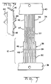
- the housing contains a plurality of sheet metal conductors 34 which are manufactured by stamping and forming, and are originally configured as a lead frame, as shown in Figure 5.
- Each lead frame contains the number of individual sheet metal conductors 34 which are required for an individual housing.
- the conductors 34 are integral at their ends with spaced apart carrier strips 38, 40 which are sheared from the ends of the conductors when the conductors are assembled to the connector housing as described below.
- each conductor 34 has a spring arm contact portion 42, an intermediate portion 44 which is located on the top wall 30 of the housing, and a lead portion 12.
- Each of the lead portions 12 comprises an adjacent portion 46, an intermediate portion 48, and an end portion 50.
- the adjacent portion 46 is adjacent to the side surface 24; the intermediate portion 48 is formed into a spring as will be described below, and the end portion 50 extends away from the side 24 of the housing and has the contact portion 14 on its extreme end.
- Barbs 37 are provided on the portions 44 of the conductors to anchor the conductors in shallow channels which extend inwardly on the housing top wall to secure them in place.
- Barbs 84 are included on the intermediate portions 48 to anchor the terminals to the rear side wall 24. The barbs are shown in greater detail in Figure 5A as including individual teeth which allow easy entry into the channels, and which lock the terminals within the channels once inserted.
- the rear side surface 24 includes a plurality of upstanding walls 100 extending outwardly therefrom which form between them, upright channels for receipt of the terminals.
- Each of the walls includes raised surfaces 104 and 106, and recessed surfaces 108, which will be described more fully herein.
- the raised surfaces 104 and 106 face each other to form constricted passageways, while the surfaces 108 face each other, but provide a larger spacing therebetween.
- the rear side surface 24 of the housing has first and second spaced apart flanges 52, 54 extending therefrom in a parallel manner relative to the board.
- Each of the flanges is integral with, and extends between two of the adjacent walls 100.
- the first flange 52 is adjacent to the mounting surface 22 while the second flange 54 is spaced from the mounting surface.
- the two spaced apart flanges 52 and 54, in combination with the two walls 100 form individual recesses 60 between the walls 100.
- each of the recesses 60 has opposed first and second recess surfaces 62, 64 which are proximate to, and spaced from, the mounting surface respectively.
- the first flange 52 has a first lip 66 at its mouth end, while the second flange has a second lip 68 at its mouth end.
- the first and second lips are at the lower and upper ends, respectively, of the channels which are provided in the first and second flanges.
- the carrier strip 40 is severed from the lead frame and the spring contact portions 42 are bent normally of the intermediate portions 44.
- the contact portions 42 are then moved downwardly through spaced apart openings 43 in the top wall 30 of the housing and the intermediate portions 44 can be moved into the shallow channels in the top wall.
- the lead portions 12 comprising terminal sections 46, 48, and 50 will then extend rearwardly beyond the back wall 24 of the housing. These lead portions are then bent downwardly and are positioned in the channels between adjacent walls 100, and adjacent to first and second lip portions 66, 68 of flange 52, 54, as shown in Figure 7.
- the barbs 84 will skive into the surfaces 108 ( Figure 9A) of the walls 100, to secure them in place prior to the final forming operation.
- a forming tool 70 is then moved against the intermediate portions 48 of the leads and serves to tuck these portions into the individual recesses 60.
- the second flange member 54 acts as a mandrel for the forming of the contact portion 48 therearound.
- the portions 48 are bent around the second lip 68 as shown and a generally U-shaped spring is thereby formed in each lead.
- the two flanges can be thought of as dies which cooperate with the tool member 70 for the forming operation.
- each spring has a first arm 72 which is adjacent to the first recess surface 62, a second arm 74 which is adjacent to the second recess surface 64, and a bight portion 76.
- the second arm 74 of each spring is connected by a transition section 78 to the associated adjacent lead portion 46.
- the portion 80 of each lead which extends from the mouth of its associated recess and over the first lip portion 66 serves as an aligning or locating portion in that it maintains the end portions 50 of the leads in coplanar relationship.
- the formed springs will be as shown in Figures 1 and 3.
- the leads are severely bent by the forming tool when the U-shaped spring members are formed and when the forming tool is withdrawn, the individual leads tend to "spring back", that is they tend to partially return to their original configuration.
- the phenomenon of spring back can be observed if one bends a piece of sheet metal through a 90 degree angle and then releases it. Depending upon the temper of the metal, the bent piece after release will move slightly back towards its original position so that the finished bent section of metal will not have a 90 degree bend. Ordinarily, this phenomenon of spring back is regarded as a problem in metal forming operations and must be taken into consideration when a stamped and formed metal part is designed.
- the very reason for providing the retention means 84 is for the spring back of the 46 which lies adjacent to the rear side wall 24, as it tends to return to its original horizontal position.
- the spring back phenomenon works to the advantage of the finished product in that the end portion 50 of each lead 12 is resiliently biased against the first lip portion 66, the locating portion, of the associated recess 60.
- the housing itself is of molded plastic material and is, for that reason, precisely dimensioned. It follows that since the aligning or locating portions of the leads are biased against the first lip portions, and the first lip portions are precisely aligned with each other, the end portions 50 of the lead and the contact portions thereof will be held in precise coplanar relationship.
- the terminals are fixedly arranged within the channels due to the side edges of the terminals in an engaging manner with the surfaces 104 and 106.
- the terminals are fixed at two points along their length, that is, between the two surfaces 104, and between the two surfaces 106. This assures that the long beam length of the terminals, due to the intermediate spring, is sufficiently supported and aligned, relative to the lateral dimension.
- the beam portion 80 is at an acute angle relative to a height of the surface 106, assuring that a long span of terminal is aligned and straightened by the constriction formed by the two facing surfaces 106 ( Figure 9A). All of the above features cooperate to assure that the contact portions 14 which extend rearwardly, and which are spaced from, the rear side wall 24 of the housing are precisely aligned and spaced laterally for precise location with the terminal pads 10 on the printed circuit board.
- each formed terminal includes a U-shaped spring, formed by the terminal portions 72, 74 and 76.
- metal spring back works to an advantage once again.
- the spring is positioned between the two flanges 52 and 54, and as the leg portion 72 of the spring is resiliently biased against the lip 66 of the flange 52, an upward reaction force is placed upon the leg 72, which carries through to leg portion 74.
- this spring force always forces the barb deeper into unskived material, as the barb is force further in its arcuate path, rather than attempting to retreat through its original footprint.
- the connector is placed upon the board, as the reaction force against the contact portion 14 will be upward, and will attempt to further seat the barb 84 within the plastic.
- the second lip portion 68 is used as a mandrel for the forming of the arcuate path of the terminal portion 74.
- the upper corner 57 of the housing is used as a mandrel for the forming of the terminal portion 46, which, as it should be noted, is of a larger radius than the forming radius of terminal portion 74.
- the removal of the terminal from the housing rear side wall 24 would not just require that the barbs skive through uncut plastic. Rather, as the barbs 84 skive through the plastic material on its original arc, the plastic material flows, or parts, to form somewhat of a channel. Thus, if the barbs were to be unseated from the rear side wall 24 of the housing the barb 84 would also have to cut through, or ride over, the plastic material which flowed to form the skived channel. Furthermore, since the removal of the terminal would require the terminal portion to swing through its original path or arc, the barbs would have to swing through the raised surface 104.
- Figure 9B shows an alternate housing where the walls have surfaces 104′ which extend lower into the housing such that when the barbs are swung in, the barbs skive into the raised surface 104′.
- Figure 8 shows an alternative embodiment in which the first lip, against which the first arm is biased, comprises an inclined surface 88 rather than a sharp edge. Under some circumstances, this alternative may be preferable.
- the lead section could be for use with through hole type terminals, the lead section includes sheared portions flanking the lead section which extends downwardly towards the board.
- the sheared sections would include barbs on their outer edges.
Landscapes
- Coupling Device And Connection With Printed Circuit (AREA)
- Multi-Conductor Connections (AREA)
Applications Claiming Priority (2)
| Application Number | Priority Date | Filing Date | Title |
|---|---|---|---|
| US07/179,604 US4850902A (en) | 1988-04-11 | 1988-04-11 | Electrical connector having improved characteristics for retaining leads to the connector housing and method of making the electrical connector |
| US179604 | 1988-04-11 |
Publications (2)
| Publication Number | Publication Date |
|---|---|
| EP0337633A1 true EP0337633A1 (de) | 1989-10-18 |
| EP0337633B1 EP0337633B1 (de) | 1994-10-05 |
Family
ID=22657256
Family Applications (1)
| Application Number | Title | Priority Date | Filing Date |
|---|---|---|---|
| EP89303191A Expired - Lifetime EP0337633B1 (de) | 1988-04-11 | 1989-03-31 | Elektrischer Verbinder mit verbesserten Eigenschaften für das Festhalten der Leiter am Verbindergehäuse |
Country Status (4)
| Country | Link |
|---|---|
| US (1) | US4850902A (de) |
| EP (1) | EP0337633B1 (de) |
| DE (1) | DE68918621T2 (de) |
| ES (1) | ES2060759T3 (de) |
Cited By (4)
| Publication number | Priority date | Publication date | Assignee | Title |
|---|---|---|---|---|
| EP0471219A3 (en) * | 1990-07-25 | 1992-07-29 | Amp Incorporated | Surface mount electrical connector and method of making the same |
| EP1341265A1 (de) * | 2002-03-01 | 2003-09-03 | Tyco Electronics Corporation | Verriegelungskontaktfahnenausrichtung |
| DE102004029052A1 (de) * | 2004-06-11 | 2006-03-09 | Walter Esser Kunststoff-Spritzgießerei GmbH & Co KG | Steckerbaugruppe |
| WO2006091961A1 (en) | 2005-02-25 | 2006-08-31 | Tyco Electronics Corporation | Surface mount header assembly having a planar alignment surface |
Families Citing this family (24)
| Publication number | Priority date | Publication date | Assignee | Title |
|---|---|---|---|---|
| GB8908098D0 (en) * | 1989-04-11 | 1989-05-24 | Amp Holland | Electrical jacks and headers |
| GB8924360D0 (en) * | 1989-10-30 | 1989-12-20 | Amp Holland | Modular jack with integral shunting means |
| JP2534861Y2 (ja) * | 1993-03-31 | 1997-05-07 | バーグ・テクノロジー・インコーポレーテッド | 電気コネクタ結合装置 |
| US5397250A (en) * | 1993-04-06 | 1995-03-14 | Amphenol Corporation | Modular jack with filter |
| JPH06310197A (ja) * | 1993-04-23 | 1994-11-04 | Matsushita Electric Works Ltd | コネクタ |
| US5401192A (en) * | 1994-03-28 | 1995-03-28 | Amphenol Corporation | Combination connector |
| US5601451A (en) * | 1994-03-28 | 1997-02-11 | Amphenol Corporation | Combination connector |
| US5792080A (en) * | 1994-05-18 | 1998-08-11 | Matsushita Electric Works, Ltd. | Massaging apparatus having self-adjusting constant strength and non-adjust strength modes |
| US5613877A (en) * | 1995-11-02 | 1997-03-25 | Molex Incorporated | Electric connector boardlock |
| US5766043A (en) * | 1996-02-29 | 1998-06-16 | Corcom, Inc. | Telephone connector |
| DE19614988A1 (de) * | 1996-04-16 | 1997-10-23 | Tridonic Bauelemente | Elektrische Anschlußvorrichtung und elektrisches Verbindungselement zur Verwendung in einer elektrischen Anschlußvorrichtung |
| US5779489A (en) * | 1996-05-24 | 1998-07-14 | The Whitaker Corporation | Board mountable electrical connector |
| US6003226A (en) * | 1997-05-14 | 1999-12-21 | Molex Incorporated | Method for manufacturing electrical connectors |
| US5885088A (en) * | 1997-07-14 | 1999-03-23 | Molex Incorporated | Electrical connector assembly with polarization means |
| US5980314A (en) * | 1998-03-13 | 1999-11-09 | Molex Incorporated | Electrical connector with improved board mounting peg |
| US6056603A (en) * | 1998-04-08 | 2000-05-02 | The Whitaker Corporation | Sacrificial plastic rib for contact retention |
| US6196879B1 (en) * | 1998-12-02 | 2001-03-06 | Stewart Connector Systems, Inc. | Surface-mountable modular electrical connector assemblies having co-planar terminals |
| KR100366413B1 (ko) * | 2000-05-15 | 2002-12-31 | 엘지전자 주식회사 | 커넥터 및 그 장착구조 |
| JP3544522B2 (ja) * | 2000-11-28 | 2004-07-21 | 日本圧着端子製造株式会社 | モジュラジャック及びその取付構造 |
| DE10246094A1 (de) † | 2002-10-02 | 2004-04-22 | Siemens Ag | Stiftleiste |
| DE102006046259B4 (de) * | 2006-09-28 | 2011-04-07 | Diehl Ako Stiftung & Co. Kg | Bauteilanordnung |
| WO2009100296A1 (en) * | 2008-02-08 | 2009-08-13 | Panduit Corp. | Communications connector with improved contacts |
| JP6447401B2 (ja) * | 2015-07-28 | 2019-01-09 | 住友電装株式会社 | コネクタ実装基板 |
| DE102016209493A1 (de) * | 2016-05-31 | 2017-11-30 | Te Connectivity Germany Gmbh | Elektrische Verbindungsbaugruppe mit überbogenem Lötstift |
Citations (2)
| Publication number | Priority date | Publication date | Assignee | Title |
|---|---|---|---|---|
| US4292736A (en) * | 1978-09-08 | 1981-10-06 | Amp Incorporated | Method for making jack type receptacles |
| FR2598856A1 (fr) * | 1986-05-15 | 1987-11-20 | Itt | Connecteur electrique pour report a plat sur carte a circuits imprimes. |
Family Cites Families (7)
| Publication number | Priority date | Publication date | Assignee | Title |
|---|---|---|---|---|
| US3754203A (en) * | 1971-07-01 | 1973-08-21 | Amp Inc | Substrate connector and terminal therefore |
| US3862792A (en) * | 1973-10-03 | 1975-01-28 | Gte Sylvania Inc | Electrical connector assembly |
| US4210376A (en) * | 1978-12-07 | 1980-07-01 | Amp Incorporated | Electrical connector receptacle |
| US4491376A (en) * | 1982-09-20 | 1985-01-01 | General Motors Corporation | Electrical header assembly |
| US4533203A (en) * | 1983-12-07 | 1985-08-06 | Amp Incorporated | Connector for printed circuit boards |
| EP0147039A3 (de) * | 1983-12-13 | 1985-08-07 | AMP INCORPORATED (a New Jersey corporation) | An einer Oberfläche montierter Verbinder |
| US4697864A (en) * | 1986-06-19 | 1987-10-06 | Amp Incorporated | Printed circuit board receptacle for sealed connector |
-
1988
- 1988-04-11 US US07/179,604 patent/US4850902A/en not_active Expired - Lifetime
-
1989
- 1989-03-31 ES ES89303191T patent/ES2060759T3/es not_active Expired - Lifetime
- 1989-03-31 DE DE68918621T patent/DE68918621T2/de not_active Expired - Fee Related
- 1989-03-31 EP EP89303191A patent/EP0337633B1/de not_active Expired - Lifetime
Patent Citations (2)
| Publication number | Priority date | Publication date | Assignee | Title |
|---|---|---|---|---|
| US4292736A (en) * | 1978-09-08 | 1981-10-06 | Amp Incorporated | Method for making jack type receptacles |
| FR2598856A1 (fr) * | 1986-05-15 | 1987-11-20 | Itt | Connecteur electrique pour report a plat sur carte a circuits imprimes. |
Cited By (6)
| Publication number | Priority date | Publication date | Assignee | Title |
|---|---|---|---|---|
| EP0471219A3 (en) * | 1990-07-25 | 1992-07-29 | Amp Incorporated | Surface mount electrical connector and method of making the same |
| EP1341265A1 (de) * | 2002-03-01 | 2003-09-03 | Tyco Electronics Corporation | Verriegelungskontaktfahnenausrichtung |
| DE102004029052A1 (de) * | 2004-06-11 | 2006-03-09 | Walter Esser Kunststoff-Spritzgießerei GmbH & Co KG | Steckerbaugruppe |
| DE102004029052B4 (de) * | 2004-06-11 | 2007-09-20 | Walter Esser Kunststoff-Spritzgießerei GmbH & Co KG | Steckerbaugruppe |
| WO2006091961A1 (en) | 2005-02-25 | 2006-08-31 | Tyco Electronics Corporation | Surface mount header assembly having a planar alignment surface |
| CN101128960B (zh) * | 2005-02-25 | 2012-07-18 | 泰科电子公司 | 具有平面对准表面的表面安装插座装置 |
Also Published As
| Publication number | Publication date |
|---|---|
| DE68918621D1 (de) | 1994-11-10 |
| US4850902A (en) | 1989-07-25 |
| DE68918621T2 (de) | 1995-05-18 |
| EP0337633B1 (de) | 1994-10-05 |
| ES2060759T3 (es) | 1994-12-01 |
Similar Documents
| Publication | Publication Date | Title |
|---|---|---|
| EP0337633B1 (de) | Elektrischer Verbinder mit verbesserten Eigenschaften für das Festhalten der Leiter am Verbindergehäuse | |
| EP0337632B1 (de) | Elektrische Einrichtung mit verbesserten Leitern für die Oberflächenmontage von gedruckten Schaltungen | |
| CA1303162C (en) | Connector with barbed boardlock | |
| US4186988A (en) | Electrical connector receptacles | |
| US5584709A (en) | Printed circuit board mounted electrical connector | |
| US5154634A (en) | Connector holding device | |
| EP0392549B1 (de) | Oberflächenmontierbarer elektrischer Verbinder | |
| JP2953585B2 (ja) | 基板取付型電気コネクタ | |
| US5145407A (en) | Mounting device for components | |
| US4354729A (en) | Preloaded electrical contact terminal | |
| JP2824764B2 (ja) | プリント回路板用のエッジカードコネクタ | |
| JPS6226557B2 (de) | ||
| WO1998018183A1 (en) | Board mountable electrical connector | |
| US4597625A (en) | Electrical connector | |
| EP0191539B1 (de) | Elektrisches Anschlussendstück für Steckverbinder | |
| US3503036A (en) | Contact terminals and manufacturing method | |
| US4296550A (en) | Method of manufacturing electrical connector receptacle | |
| US5860838A (en) | Tangle-preventive mechanism in three contact pieces type contact | |
| JP3681173B2 (ja) | Smt型dinコネクタ | |
| EP0009867A1 (de) | Elektrische Steckdose, die einen stöpselartigen Stecker aufnehmen kann, und Verfahren zur Herstellung dieser Steckdose | |
| USRE35735E (en) | Connector with barbed boardlock | |
| JPH0817099B2 (ja) | 表面実装型電気部品およびその製造方法 | |
| US4790771A (en) | Wire trap terminal | |
| US6419518B1 (en) | Insulation displacement contact for use with fine wires | |
| EP0878879B1 (de) | Verfahren zur Herstellung von elektrischen Verbindern und Verbinder |
Legal Events
| Date | Code | Title | Description |
|---|---|---|---|
| PUAI | Public reference made under article 153(3) epc to a published international application that has entered the european phase |
Free format text: ORIGINAL CODE: 0009012 |
|
| AK | Designated contracting states |
Kind code of ref document: A1 Designated state(s): CH DE ES FR GB IT LI NL SE |
|
| RAP1 | Party data changed (applicant data changed or rights of an application transferred) |
Owner name: AMP INCORPORATED |
|
| 17P | Request for examination filed |
Effective date: 19900315 |
|
| 17Q | First examination report despatched |
Effective date: 19920714 |
|
| RAP1 | Party data changed (applicant data changed or rights of an application transferred) |
Owner name: THE WHITAKER CORPORATION |
|
| GRAA | (expected) grant |
Free format text: ORIGINAL CODE: 0009210 |
|
| AK | Designated contracting states |
Kind code of ref document: B1 Designated state(s): CH DE ES FR GB IT LI NL SE |
|
| REF | Corresponds to: |
Ref document number: 68918621 Country of ref document: DE Date of ref document: 19941110 |
|
| REG | Reference to a national code |
Ref country code: ES Ref legal event code: FG2A Ref document number: 2060759 Country of ref document: ES Kind code of ref document: T3 |
|
| ET | Fr: translation filed | ||
| ITF | It: translation for a ep patent filed | ||
| EAL | Se: european patent in force in sweden |
Ref document number: 89303191.4 |
|
| PLBE | No opposition filed within time limit |
Free format text: ORIGINAL CODE: 0009261 |
|
| STAA | Information on the status of an ep patent application or granted ep patent |
Free format text: STATUS: NO OPPOSITION FILED WITHIN TIME LIMIT |
|
| 26N | No opposition filed | ||
| PGFP | Annual fee paid to national office [announced via postgrant information from national office to epo] |
Ref country code: NL Payment date: 19981222 Year of fee payment: 11 |
|
| PGFP | Annual fee paid to national office [announced via postgrant information from national office to epo] |
Ref country code: GB Payment date: 19990203 Year of fee payment: 11 |
|
| PGFP | Annual fee paid to national office [announced via postgrant information from national office to epo] |
Ref country code: FR Payment date: 19990302 Year of fee payment: 11 |
|
| PGFP | Annual fee paid to national office [announced via postgrant information from national office to epo] |
Ref country code: SE Payment date: 19990303 Year of fee payment: 11 |
|
| PGFP | Annual fee paid to national office [announced via postgrant information from national office to epo] |
Ref country code: ES Payment date: 19990322 Year of fee payment: 11 |
|
| PGFP | Annual fee paid to national office [announced via postgrant information from national office to epo] |
Ref country code: DE Payment date: 19990330 Year of fee payment: 11 |
|
| PGFP | Annual fee paid to national office [announced via postgrant information from national office to epo] |
Ref country code: CH Payment date: 19990422 Year of fee payment: 11 |
|
| PG25 | Lapsed in a contracting state [announced via postgrant information from national office to epo] |
Ref country code: LI Free format text: LAPSE BECAUSE OF NON-PAYMENT OF DUE FEES Effective date: 20000331 Ref country code: GB Free format text: LAPSE BECAUSE OF NON-PAYMENT OF DUE FEES Effective date: 20000331 Ref country code: CH Free format text: LAPSE BECAUSE OF NON-PAYMENT OF DUE FEES Effective date: 20000331 |
|
| PG25 | Lapsed in a contracting state [announced via postgrant information from national office to epo] |
Ref country code: SE Free format text: LAPSE BECAUSE OF NON-PAYMENT OF DUE FEES Effective date: 20000401 Ref country code: ES Free format text: LAPSE BECAUSE OF NON-PAYMENT OF DUE FEES Effective date: 20000401 |
|
| PG25 | Lapsed in a contracting state [announced via postgrant information from national office to epo] |
Ref country code: NL Free format text: LAPSE BECAUSE OF NON-PAYMENT OF DUE FEES Effective date: 20001001 |
|
| REG | Reference to a national code |
Ref country code: CH Ref legal event code: PL |
|
| GBPC | Gb: european patent ceased through non-payment of renewal fee |
Effective date: 20000331 |
|
| PG25 | Lapsed in a contracting state [announced via postgrant information from national office to epo] |
Ref country code: FR Free format text: LAPSE BECAUSE OF NON-PAYMENT OF DUE FEES Effective date: 20001130 |
|
| NLV4 | Nl: lapsed or anulled due to non-payment of the annual fee |
Effective date: 20001001 |
|
| EUG | Se: european patent has lapsed |
Ref document number: 89303191.4 |
|
| REG | Reference to a national code |
Ref country code: FR Ref legal event code: ST |
|
| PG25 | Lapsed in a contracting state [announced via postgrant information from national office to epo] |
Ref country code: DE Free format text: LAPSE BECAUSE OF NON-PAYMENT OF DUE FEES Effective date: 20010103 |
|
| REG | Reference to a national code |
Ref country code: ES Ref legal event code: FD2A Effective date: 20010910 |
|
| PG25 | Lapsed in a contracting state [announced via postgrant information from national office to epo] |
Ref country code: IT Free format text: LAPSE BECAUSE OF NON-PAYMENT OF DUE FEES;WARNING: LAPSES OF ITALIAN PATENTS WITH EFFECTIVE DATE BEFORE 2007 MAY HAVE OCCURRED AT ANY TIME BEFORE 2007. THE CORRECT EFFECTIVE DATE MAY BE DIFFERENT FROM THE ONE RECORDED. Effective date: 20050331 |