EP0338528B1 - Halbleiterspeicher - Google Patents
Halbleiterspeicher Download PDFInfo
- Publication number
- EP0338528B1 EP0338528B1 EP89107021A EP89107021A EP0338528B1 EP 0338528 B1 EP0338528 B1 EP 0338528B1 EP 89107021 A EP89107021 A EP 89107021A EP 89107021 A EP89107021 A EP 89107021A EP 0338528 B1 EP0338528 B1 EP 0338528B1
- Authority
- EP
- European Patent Office
- Prior art keywords
- refresh
- signal
- necessary
- execution
- counter
- Prior art date
- Legal status (The legal status is an assumption and is not a legal conclusion. Google has not performed a legal analysis and makes no representation as to the accuracy of the status listed.)
- Expired - Lifetime
Links
- 239000004065 semiconductor Substances 0.000 title claims description 17
- 230000015654 memory Effects 0.000 claims description 27
- 230000004044 response Effects 0.000 claims description 9
- 238000010586 diagram Methods 0.000 description 5
- 230000000694 effects Effects 0.000 description 4
- 238000010276 construction Methods 0.000 description 3
- 230000008859 change Effects 0.000 description 2
- 230000003068 static effect Effects 0.000 description 2
- 230000000593 degrading effect Effects 0.000 description 1
- 230000006870 function Effects 0.000 description 1
- 230000004048 modification Effects 0.000 description 1
- 238000012986 modification Methods 0.000 description 1
- 230000002093 peripheral effect Effects 0.000 description 1
- 238000000926 separation method Methods 0.000 description 1
Images



Classifications
-
- G—PHYSICS
- G11—INFORMATION STORAGE
- G11C—STATIC STORES
- G11C11/00—Digital stores characterised by the use of particular electric or magnetic storage elements; Storage elements therefor
- G11C11/21—Digital stores characterised by the use of particular electric or magnetic storage elements; Storage elements therefor using electric elements
- G11C11/34—Digital stores characterised by the use of particular electric or magnetic storage elements; Storage elements therefor using electric elements using semiconductor devices
- G11C11/40—Digital stores characterised by the use of particular electric or magnetic storage elements; Storage elements therefor using electric elements using semiconductor devices using transistors
- G11C11/401—Digital stores characterised by the use of particular electric or magnetic storage elements; Storage elements therefor using electric elements using semiconductor devices using transistors forming cells needing refreshing or charge regeneration, i.e. dynamic cells
- G11C11/406—Management or control of the refreshing or charge-regeneration cycles
-
- G—PHYSICS
- G11—INFORMATION STORAGE
- G11C—STATIC STORES
- G11C11/00—Digital stores characterised by the use of particular electric or magnetic storage elements; Storage elements therefor
- G11C11/21—Digital stores characterised by the use of particular electric or magnetic storage elements; Storage elements therefor using electric elements
- G11C11/34—Digital stores characterised by the use of particular electric or magnetic storage elements; Storage elements therefor using electric elements using semiconductor devices
- G11C11/40—Digital stores characterised by the use of particular electric or magnetic storage elements; Storage elements therefor using electric elements using semiconductor devices using transistors
- G11C11/401—Digital stores characterised by the use of particular electric or magnetic storage elements; Storage elements therefor using electric elements using semiconductor devices using transistors forming cells needing refreshing or charge regeneration, i.e. dynamic cells
- G11C11/403—Digital stores characterised by the use of particular electric or magnetic storage elements; Storage elements therefor using electric elements using semiconductor devices using transistors forming cells needing refreshing or charge regeneration, i.e. dynamic cells with charge regeneration common to a multiplicity of memory cells, i.e. external refresh
-
- G—PHYSICS
- G11—INFORMATION STORAGE
- G11C—STATIC STORES
- G11C11/00—Digital stores characterised by the use of particular electric or magnetic storage elements; Storage elements therefor
- G11C11/21—Digital stores characterised by the use of particular electric or magnetic storage elements; Storage elements therefor using electric elements
- G11C11/34—Digital stores characterised by the use of particular electric or magnetic storage elements; Storage elements therefor using electric elements using semiconductor devices
- G11C11/40—Digital stores characterised by the use of particular electric or magnetic storage elements; Storage elements therefor using electric elements using semiconductor devices using transistors
- G11C11/401—Digital stores characterised by the use of particular electric or magnetic storage elements; Storage elements therefor using electric elements using semiconductor devices using transistors forming cells needing refreshing or charge regeneration, i.e. dynamic cells
- G11C11/4063—Auxiliary circuits, e.g. for addressing, decoding, driving, writing, sensing or timing
- G11C11/407—Auxiliary circuits, e.g. for addressing, decoding, driving, writing, sensing or timing for memory cells of the field-effect type
- G11C11/4076—Timing circuits
Definitions
- the present invention relates to a semiconductor memory having dynamic memory cells, and more particularly to improved control for refresh operation of such semiconductor memories.
- PS RAM pseudo static RAM
- Conventional refresh operation for a dynamic memory cell such as a PS RAM includes the three types of operation of chip-only refresh, auto refresh and self refresh.
- chip-only refresh operation a refresh address is supplied to a memory externally to effect dummy access and then refresh operation.
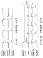
- auto refresh operation a refresh address counter is incorporated into a RAM to supply to its refresh terminal a refresh request signal clocked externally as shown in the timing chart of Fig. 1, to thus effect refresh operation each time the refresh request signal is input.
- the refresh period is determined in accordance with the period of the refresh request signals.
- a refresh address counter and timer are included in the RAM to drive the timer while maintaining the external refresh request signal at the low (L) level as shown in the timing chart of Fig. 2, to therefore effect refresh operation for each carry-over cycle of the timer.
- the refresh cycle is determined in accordance with the count cycle of the internal timer counter.
- FIG. 3 An example of a computer system using PS RAM is shown in Fig. 3.
- a chip enable signal ROM-CE of, e.g., ROM 2 as a refresh request signal, auto refresh operation is performed at each operation code fetch cycle of CPU 1.
- an auto refresh operation is performed by supplying a refresh request signal at each operation code fetch cycle.
- all PS RAM are refreshed as required and so a large refresh current is required.
- the system power supply is accordingly required to be made large, hindering the system from being made compact and from saving energy.
- the refresh current be several times as large as the operation current of PS RAMs of a large system which consumes an operation current corresponding only to 1 to 2 chips.
- EP-A-0164735 describes a microprocessor including an execution unit executing a program according to an instruction, an instruction prefetch circuit storing a plurality of instructions to be executed by the execution unit, a refresh control circuit controlling a refresh operation of a dynamic memory coupled to an external bus and a control unit.
- the control unit receives bus access request signals from the execution unit and from the instruction prefetch circuit, respectively, and a refresh request signal from the refresh control circuit and sends a refresh grant signal to the refresh control circuit in response to the refresh request signal when both the bus access request signals are absent.
- the refresh control circuit may generate a first refresh request signal and a second refresh request signal.
- the control unit in this case, generates the refresh grant signal in response to the first refresh request signal only when both the bus access request signals from the execution unit and the instruction prefetch circuit are absent, but generates the refresh grant signal at any time when the second refresh request signal is generated.
- This refresh control circuit may be adapted to a microprocessor having no instruction prefetch circuit.
- JP-A-58-182193 describes a refresh controller for a memory which includes an oscillator for generating the refresh request at specific intervals of time.
- a CRT display device accesses the memory the refresh request is rendered ineffective but a counter circuit counts the number of ineffective refresh request signals. After the access has been terminated the refresh operation is repeated sequentially until the counter is reduced to zero.
- the refresh control logic uses a counter to timeout periodically and indicate the need for a refresh cycle. This counter times out 128 times per total refresh period. The timeouts and subsequent refresh cycles are generally spread evenly across the total refresh period in order to minimize the impact of refresh on the power supply and to minimize the reliability impact.
- a timeout occurs, a flip-flop is set and the refresh control logic looks for a refresh allowed signal from the data flow control logic. The refresh allowed signal normally occurs before a subsequent timeout occurs. When the refresh allowed signal occurs, the refresh control logic executes a refresh cycle and then waits for the next timeout to occur.
- a similar situation occurs during the cycle steal operations where the cycle steal memory access is interleaved with the refresh access for cycle steal write operations. These operations occur in a burst mode.
- the data available signal indicates that data has been written into the addressed memory location and that a new location can be addressed.
- the storage cycle request signal initiates a subsequent cycle steal operation. Because a window of time exists during which the processor is establishing the next storage address and preparing the data for writing at that address, a refresh cycle can occur without degrading the system performance. There are three refresh modes including allowed refresh mode, forced refresh mode and emergency refresh mode. It should be noted that the associated hidden refresh cycle is interleaved with functional memory accesses during cycle steal read operations. The refresh cycle can occur after a functional read or memory access and before the processor logic establishes the address for the next cycle steal operation.
- the refresh control logic forces a refresh cycle.
- the refresh logic reverts to the allowed refresh mode immediately after a refresh cycle is taken in the forced refresh mode.
- refresh operation is alternated between two RAM banks and is permitted to occur during processor cycles in which the bank currently identified for refresh is not selected for a read or write operation by the processor.
- the time from the most recent refresh is accumulated and no further refresh cycle is initiated until the accumulated time exceeds a fixed period that is short of or half the maximum allowable refresh separation interval by a preselected margin.
- a semiconductor dynamic random access type memory having dynamic memory cells, said semiconductor dynamic memory comprising: timer means for outputting a signal at every predetermined period necessary to refresh the dynamic memory cells, means for outputting a refresh execution signal in response to a refresh request signal supplied from an external circuit only when it is necessary to refresh the dynamic memory cells, means for executing a refresh operation in response to said refresh execution signal, and number storage means for storing, as a necessary-refresh-number, the number of said signals output from said timer means during the time when said refresh operation is not executed, characterized in that said means for outputting comprises refresh execution determining means for output of said refresh execution signals equal in number to said necessary-refresh-number in response to the same number of said refresh request signals.
- the refresh operation of this invention has both the advantages of conventional auto refresh and self refresh operations.
- the determining means comprises a timer and a flip-flop.
- the timer generates a signal at every predetermined period.
- the flip-flop is set by the output signal from the timer, receives a refresh request signal only under a set state thereof to generate a refresh execution signal, and is reset after completion of refresh operation.
- the refresh period is determined by the period of the timer output signals so that a suitable refresh period can be set as desired.
- the determining means comprises a timer, a necessary refresh number storage unit, and a refresh execution determining unit.
- the timer generates a signal at every predetermined period.
- the necessary refresh number storage unit stores, as the necessary refresh number, the number of timer output signals output during the time when refresh operation is not executed.
- the refresh execution determining unit receives a refresh request signal from an external circuit and outputs refresh execution signals equal in number to the necessary refresh number.
- a suitable refresh period can be set as desired by setting the period of timer output signals. Furthermore, even if a refresh request signal is not generated and refresh operation is intercepted because of system stoppage, the number of refresh operations not executed is stored as the necessary refresh number. Upon input of a refresh request signal, refresh operations equal in number to the necessary refresh number are executed for replenishment. Therefore, stored data are not changed or lost and stable system operation is ensured.
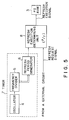
- Fig. 5 is a block diagram showing the circuit arrangement of a semiconductor memory useful in understanding the present invention.
- the circuit is constructed of a timer 7, refresh execution determining unit 8 and PS RAMs 3.
- the timer 7 is comprised by an oscillator 4, frequency divider 5 and refresh period generator 6, and generates a pulse signal at every predetermined period.
- the refresh execution determining unit 8 determines, each time upon reception of the pulse signal from the timer 7, whether or not a refresh operation is necessary, and only when it is determined necessary, generates a refresh execution signal in response to a refresh request signal from an external circuit.
- a timer of a PS RAM operates only when a refresh request signal is at the low "L" level. However, in this circuit, the timer 7 operates continuously.
- the refresh request determining unit 8 is constructed of a flip-flop (F/F) circuit which is set by the output pulse from the timer 7.
- F/F flip-flop
- PS RAM 3 has the same circuit arrangement as conventional PS RAM chip so that upon reception of the refresh execution signal at its refresh terminal, a refresh operation is executed.
- the refresh execution signal also operates to reset the refresh execution determining unit 8.
- the refresh request signal is supplied at each operation code fetch cycle of CPU 1.
- a pulse is. output from the timer 7 at every predetermined period to match the need for refresh operation for the devices.
- the refresh execution determining unit (F/F) 8 is set. Only under this set state, the F/F 8 responds to the refresh request signal and outputs the refresh execution signal to effect refresh operation. After completion of this refresh operation, the refresh execution determining unit (F/F) 8 is reset. During the time duration from this resetting to the next setting, any refresh request signal is not accepted to F/F 8 and hence refresh operation is not executed.
- Fig. 7 shows the circuit arrangement of an embodiment of a semiconductor memory in which a backup function for such a case is added.
- like elements to those shown in Fig. 5 are represented by using identical reference numerals.
- the characteristic feature of this embodiment is to provide a necessary-refresh-number storage unit 9 and refresh execution determining unit 10.
- the storage unit 9 stores, as the necessary-refresh-number, the number of refresh operations cancelled out due to there being no refresh request signal for the time duration longer than the period of output pulses from the timer 7.
- the. refresh execution determining unit 10 Upon receipt of a new refresh request signal from the external, the. refresh execution determining unit 10 outputs refresh execution signals equal in number to the necessary-refresh-number stored in the storage unit 9.
- the storage unit 9 is constructed of an up/down counter which counts up an output pulse from the timer 7, and counts down a refresh execution signal so that the count value thereof represents the necessary-refresh-number.
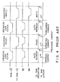
- refresh request signals are output in a dispersed manner such that two refresh request signals are output after output pulse P1 from the timer 7, and after a lapse of certain time duration, two refresh pulses are output after pulse P2, and one refresh pulse signal after pulse P4.
- the count value of the storage unit 9 becomes 1 upon receipt of pulse P1.
- the refresh execution determining unit 10 outputs one refresh execution signal to therefore execute a refresh operation once.
- the count value of the storage unit 9 becomes 0 so that a refresh execution signal is not outputted for the next refresh request signal and a refresh operation is not executed accordingly.
- the count value of the necessary refresh number storage unit 9 becomes 2 so that at the next refresh request signal, two refresh execution signals are output and the refresh operation is executed two times consecutively.
- the refresh request pulse is not output after pulses P5, P6 and P7, but it is output for the first time after pulse P8.
- the count value of the storage unit 9 becomes 4 upon receipt of pulses P5 to P8. Therefore, upon receipt of the next refresh request signal, the refresh request signal is output four times consecutively to execute the refresh operation concentrically. Thereafter, in the similar manner to the case shown in Fig. 8(a), an auto refresh operation is executed at each refresh request signal after pulses P9 and P10.
- replenishing auto refresh operations equal in number to the necessary-refresh-number are carried out, so that it is expected that there is no fear of change or loss of data and that stable system operation is ensured.
- the necessary-refresh-number storage unit 9 has been realized using an up/down counter which has a rather complex circuit arrangement and requires a large space therefor.
- the counter for storing the necessary-refresh-number is realized using an up-counter similar in construction to a refresh address counter to make the circuit simple and small, an embodiment of which is shown in Fig. 9.
- a refresh address counter 11, up-counter 12 and refresh execution determining unit 13 The refresh address counter 11 has the same construction as that of a refresh address counter used with conventional PS RAM or DRAM, and increments its address value upon execution of a refresh operation, as well known in the art.
- the up-counter 12 having the same construction as that of the refresh address counter 11 counts up an output pulse from the timer 7.
- the refresh execution determining unit 13 Upon reception of a refresh request signal, the refresh execution determining unit 13 outputs refresh execution signals concentratedly until the count value of the up-counter becomes equal to the address value of the refresh address counter 11.
- the count value of the up-counter 12 is larger than the address value of the refresh address counter 11 by the amount corresponding to the number of cancelled refresh operations.
- the difference between the address value and count value represents the necessary-refresh-number.
- the refresh operations are executed concentratedly upon receipt of the next refresh request signal until the difference becomes 0, i.e., necessary-refresh-number times.
- the operation of this embodiment is substantially the same as that of the embodiment of Fig. 7 described with Fig. 8.
- comparison between the address and count values is carried out each time the refresh request signal is supplied.
- a modification is applicable, wherein the comparison is carried out continuously to always check the necessary-refresh-number and only when the number is not zero, is refresh request signal accepted and the necessary number of refresh operations executed.
- the semiconductor memory of this invention determines whether or not a refresh operation is necessary, and executes a refresh operation only when necessary. Therefore, unnecessary refresh operation can be dispensed with to therefore reduce a load of power supply.
Landscapes
- Engineering & Computer Science (AREA)
- Microelectronics & Electronic Packaging (AREA)
- Computer Hardware Design (AREA)
- Dram (AREA)
- Semiconductor Memories (AREA)
Claims (4)
- Dynamischer Halbleiterspeicher mit wahlfreiem Zugriff (RAM), welcher dynamische Speicherzellen (3) aufweist,
wobei der dynamische Halbleiterspeicher aufweist:
eine Zeitgebervorrichtung (7) zur Ausgabe eines Signals in jedem vorbestimmten Zeitraum, der zum Auffrischen der dynamischen Speicherzellen erforderlich ist,
eine Vorrichtung (10, 13) zur Ausgabe eines Auffrischausführungssignals in Reaktion auf ein Auffrischanforderungssignal, welches von einer externen Schaltung geliefert wird, nur dann, wenn es erforderlich ist, die dynamischen Speicherzellen aufzufrischen;
eine Vorrichtung (3) zur Ausführung eines Auffrischvorgangs in Reaktion auf das Auffrischausführungssignal, und eine Anzahlspeichervorrichtung (9, 11, 12) zum Speichern, als erforderliche Auffrischanzahl, der Anzahl der Signale, die von der Zeitgebervorrichtung (7) während jener Zeit ausgegeben werden, wenn der Auffrischvorgang nicht durchgeführt wird, dadurch gekennzeichnet, daß die Vorrichtung (10, 13) zur Ausgabe eine Auffrischausführungs-Festlegungsvorrichtung (10, 13) zur Ausgabe der Auffrischausführungssignale in gleicher Anzahl wie die erforderliche Auffrischanzahl in Reaktion auf dieselbe Anzahl der Auffrischanforderungssignale aufweist. - Dynamischer Halbleiterspeicher mit wahlfreiem Zugriff nach Anspruch 1, dadurch gekennzeichnet, daß die Vorrichtung zur Ausgabe (10, 13) eine Flipflopvorrichtung aufweist, die durch das Signal von der Zeitgebervorrichtung (7) gesetzt wird, das Auffrischanforderungssignal nur in ihrem gesetzten Zustand empfängt, um das Auffrischausführungssignal zu erzeugen, und nach Beendigung des Auffrischvorgangs zurückgesetzt wird.
- Dynamischer Halbleiterspeicher mit wahlfreiem Zugriff nach Anspruch 1 oder 2, dadurch gekennzeichnet, daß die Speichervorrichtung (9) für die erforderliche Auffrischanzahl einen Aufwärts/Abwärtszähler aufweist, der das von der Zeitgebervorrichtung (7) ausgegebene Signal heraufzählt, und das Auffrischausführungssignal herunterzählt, wobei der Zählwert des Aufwärts/Abwärtszählers die erforderliche Auffrischanzahl ist.
- Dynamicher Halbleiterspeicher mit wahlfreiem Zugriff nach Anspruch 1 oder 2, dadurch gekennzeichnet, daß die Speichervorrichtung (11, 12) für die erforderliche Auffrischanzahl eine Aufwärts/Abwärtszähler (12) zum Heraufzählen des Signals aufweist, welches von der Zeitgebervorrichtung (7) ausgegeben wird, und einen Auffrischadressenzähler (11), der seinen Adressenwert schrittweise nach Ausführung des Auffrischvorgangs erhöht, wobei eine Differenz zwischen dem Zählwert des Aufwärtszählers und dem Adressenwert des Auffrischadressenzählers die erforderliche Auffrischanzahl ist.
Applications Claiming Priority (2)
| Application Number | Priority Date | Filing Date | Title |
|---|---|---|---|
| JP96147/88 | 1988-04-19 | ||
| JP63096147A JPH01267896A (ja) | 1988-04-19 | 1988-04-19 | 半導体メモリ |
Publications (3)
| Publication Number | Publication Date |
|---|---|
| EP0338528A2 EP0338528A2 (de) | 1989-10-25 |
| EP0338528A3 EP0338528A3 (de) | 1991-11-13 |
| EP0338528B1 true EP0338528B1 (de) | 1995-08-23 |
Family
ID=14157269
Family Applications (1)
| Application Number | Title | Priority Date | Filing Date |
|---|---|---|---|
| EP89107021A Expired - Lifetime EP0338528B1 (de) | 1988-04-19 | 1989-04-19 | Halbleiterspeicher |
Country Status (5)
| Country | Link |
|---|---|
| US (1) | US5027327A (de) |
| EP (1) | EP0338528B1 (de) |
| JP (1) | JPH01267896A (de) |
| KR (1) | KR890016677A (de) |
| DE (1) | DE68923899T2 (de) |
Families Citing this family (16)
| Publication number | Priority date | Publication date | Assignee | Title |
|---|---|---|---|---|
| JPH0778991B2 (ja) * | 1988-07-26 | 1995-08-23 | 株式会社東芝 | 半導体メモリ |
| JP2898016B2 (ja) * | 1989-06-23 | 1999-05-31 | 新日本製鐵株式会社 | メモリ装置 |
| US5193165A (en) * | 1989-12-13 | 1993-03-09 | International Business Machines Corporation | Memory card refresh buffer |
| JPH04141886A (ja) * | 1990-10-01 | 1992-05-15 | Nec Corp | マイクロコンピュータ |
| JP3225531B2 (ja) * | 1990-05-15 | 2001-11-05 | セイコーエプソン株式会社 | メモリカード |
| KR100274704B1 (ko) * | 1990-05-15 | 2000-12-15 | 야마무라 가쓰미 | 메모리 카드 및 dram 메모리 카드 |
| EP0547758B1 (de) * | 1991-12-18 | 1999-01-20 | Sun Microsystems, Inc. | Wahlfreie Auffrischung |
| JP3426693B2 (ja) * | 1994-03-07 | 2003-07-14 | 株式会社日立製作所 | 半導体記憶装置 |
| KR0129197B1 (ko) * | 1994-04-21 | 1998-10-01 | 문정환 | 메모리셀어레이의 리플레쉬 제어회로 |
| JP3165585B2 (ja) * | 1994-05-13 | 2001-05-14 | シャープ株式会社 | 情報処理装置 |
| US6025741A (en) * | 1996-12-23 | 2000-02-15 | International Business Machines Corporation | Conditional restore for execution unit |
| US7930471B2 (en) | 2004-11-24 | 2011-04-19 | Qualcomm Incorporated | Method and system for minimizing impact of refresh operations on volatile memory performance |
| JP4664126B2 (ja) * | 2005-06-14 | 2011-04-06 | 富士通セミコンダクター株式会社 | 半導体メモリ |
| JP4934118B2 (ja) * | 2008-09-05 | 2012-05-16 | ルネサスエレクトロニクス株式会社 | 半導体記憶装置 |
| JP2015032325A (ja) * | 2013-07-31 | 2015-02-16 | マイクロン テクノロジー, インク. | 半導体装置 |
| FR3094830A1 (fr) * | 2019-04-08 | 2020-10-09 | Proton World International N.V. | Circuit d'alimentation d'une mémoire volatile |
Family Cites Families (5)
| Publication number | Priority date | Publication date | Assignee | Title |
|---|---|---|---|---|
| US4292676A (en) * | 1978-11-15 | 1981-09-29 | Lockheed Electronics Co., Inc. | Refresh cycle minimizer in a dynamic semiconductor memory |
| EP0116774B1 (de) * | 1982-12-27 | 1991-07-24 | Kabushiki Kaisha Toshiba | Halbleiterspeicheranordnung mit einem Auffrischungsmechanismus |
| US4672583A (en) * | 1983-06-15 | 1987-06-09 | Nec Corporation | Dynamic random access memory device provided with test circuit for internal refresh circuit |
| US4625301A (en) * | 1983-11-30 | 1986-11-25 | Tandy Corporation | Dynamic memory refresh circuit |
| EP0164735A3 (de) * | 1984-06-11 | 1988-11-09 | Nec Corporation | Mikroprozessor mit Erfrischungsschaltung für dynamischen Speicher |
-
1988
- 1988-04-19 JP JP63096147A patent/JPH01267896A/ja active Pending
-
1989
- 1989-04-18 US US07/339,661 patent/US5027327A/en not_active Expired - Lifetime
- 1989-04-19 DE DE68923899T patent/DE68923899T2/de not_active Expired - Fee Related
- 1989-04-19 KR KR1019890005152A patent/KR890016677A/ko not_active Ceased
- 1989-04-19 EP EP89107021A patent/EP0338528B1/de not_active Expired - Lifetime
Also Published As
| Publication number | Publication date |
|---|---|
| KR890016677A (ko) | 1989-11-29 |
| US5027327A (en) | 1991-06-25 |
| JPH01267896A (ja) | 1989-10-25 |
| EP0338528A3 (de) | 1991-11-13 |
| EP0338528A2 (de) | 1989-10-25 |
| DE68923899D1 (de) | 1995-09-28 |
| DE68923899T2 (de) | 1996-03-14 |
Similar Documents
| Publication | Publication Date | Title |
|---|---|---|
| EP0338528B1 (de) | Halbleiterspeicher | |
| US5262998A (en) | Dynamic random access memory with operational sleep mode | |
| KR100266885B1 (ko) | 메모리 리프레시 시스템 | |
| US6956782B2 (en) | Selective bank refresh | |
| US6212599B1 (en) | Method and apparatus for a memory control system including a secondary controller for DRAM refresh during sleep mode | |
| US6879536B2 (en) | Semiconductor memory device and system outputting refresh flag | |
| US20080270683A1 (en) | Systems and methods for a dram concurrent refresh engine with processor interface | |
| KR0169288B1 (ko) | 컴퓨터 시스템 및 그 메모리를 리프레싱하기 위한 방법 | |
| EP0164735A2 (de) | Mikroprozessor mit Erfrischungsschaltung für dynamischen Speicher | |
| EP0547758B1 (de) | Wahlfreie Auffrischung | |
| JP3225531B2 (ja) | メモリカード | |
| US5583823A (en) | Dram refresh circuit | |
| US5808952A (en) | Adaptive auto refresh | |
| US6721225B2 (en) | Semiconductor memory device with activation of a burst refresh when a long cycle is detected | |
| US4313180A (en) | Refresh system for a dynamic memory | |
| US20050078538A1 (en) | Selective address-range refresh | |
| US20010040833A1 (en) | Method and apparatus for self timing refresh | |
| JP2590712B2 (ja) | メモリ制御装置 | |
| JP2594757B2 (ja) | 記憶装置のリフレッシュ制御回路 | |
| EP0457310A2 (de) | Speicherkarte | |
| US20020133677A1 (en) | Digital data processing system | |
| JP2000123568A (ja) | Dramリフレッシュ制御回路およびリフレッシュ制御回路を内蔵したdram | |
| JPH01211397A (ja) | 記憶装置のリフレッシュ装置 | |
| JPH01208796A (ja) | ダイナミックメモリのリフレッシュ制御装置 | |
| JPH05135577A (ja) | 半導体記憶装置 |
Legal Events
| Date | Code | Title | Description |
|---|---|---|---|
| PUAI | Public reference made under article 153(3) epc to a published international application that has entered the european phase |
Free format text: ORIGINAL CODE: 0009012 |
|
| 17P | Request for examination filed |
Effective date: 19890419 |
|
| AK | Designated contracting states |
Kind code of ref document: A2 Designated state(s): DE FR GB |
|
| PUAL | Search report despatched |
Free format text: ORIGINAL CODE: 0009013 |
|
| AK | Designated contracting states |
Kind code of ref document: A3 Designated state(s): DE FR GB |
|
| 17Q | First examination report despatched |
Effective date: 19921124 |
|
| GRAA | (expected) grant |
Free format text: ORIGINAL CODE: 0009210 |
|
| AK | Designated contracting states |
Kind code of ref document: B1 Designated state(s): DE FR GB |
|
| REF | Corresponds to: |
Ref document number: 68923899 Country of ref document: DE Date of ref document: 19950928 |
|
| ET | Fr: translation filed | ||
| PLBE | No opposition filed within time limit |
Free format text: ORIGINAL CODE: 0009261 |
|
| STAA | Information on the status of an ep patent application or granted ep patent |
Free format text: STATUS: NO OPPOSITION FILED WITHIN TIME LIMIT |
|
| 26N | No opposition filed | ||
| REG | Reference to a national code |
Ref country code: GB Ref legal event code: 746 Effective date: 19981010 |
|
| REG | Reference to a national code |
Ref country code: FR Ref legal event code: D6 |
|
| REG | Reference to a national code |
Ref country code: GB Ref legal event code: IF02 |
|
| PGFP | Annual fee paid to national office [announced via postgrant information from national office to epo] |
Ref country code: DE Payment date: 20070412 Year of fee payment: 19 |
|
| PGFP | Annual fee paid to national office [announced via postgrant information from national office to epo] |
Ref country code: GB Payment date: 20070418 Year of fee payment: 19 |
|
| PGFP | Annual fee paid to national office [announced via postgrant information from national office to epo] |
Ref country code: FR Payment date: 20070411 Year of fee payment: 19 |
|
| GBPC | Gb: european patent ceased through non-payment of renewal fee |
Effective date: 20080419 |
|
| PG25 | Lapsed in a contracting state [announced via postgrant information from national office to epo] |
Ref country code: DE Free format text: LAPSE BECAUSE OF NON-PAYMENT OF DUE FEES Effective date: 20081101 |
|
| REG | Reference to a national code |
Ref country code: FR Ref legal event code: ST Effective date: 20081231 |
|
| PG25 | Lapsed in a contracting state [announced via postgrant information from national office to epo] |
Ref country code: FR Free format text: LAPSE BECAUSE OF NON-PAYMENT OF DUE FEES Effective date: 20080430 |
|
| PG25 | Lapsed in a contracting state [announced via postgrant information from national office to epo] |
Ref country code: GB Free format text: LAPSE BECAUSE OF NON-PAYMENT OF DUE FEES Effective date: 20080419 |