EP0339732A1 - Verfahren zur Herstellung einer auf einem N-Typ-Substrat integrierten Schaltung, umfassend vertikale PNP- und NPN-Transistoren, die voneinander isoliert sind - Google Patents
Verfahren zur Herstellung einer auf einem N-Typ-Substrat integrierten Schaltung, umfassend vertikale PNP- und NPN-Transistoren, die voneinander isoliert sind Download PDFInfo
- Publication number
- EP0339732A1 EP0339732A1 EP89201041A EP89201041A EP0339732A1 EP 0339732 A1 EP0339732 A1 EP 0339732A1 EP 89201041 A EP89201041 A EP 89201041A EP 89201041 A EP89201041 A EP 89201041A EP 0339732 A1 EP0339732 A1 EP 0339732A1
- Authority
- EP
- European Patent Office
- Prior art keywords
- region
- type
- regions
- pnp
- npn
- Prior art date
- Legal status (The legal status is an assumption and is not a legal conclusion. Google has not performed a legal analysis and makes no representation as to the accuracy of the status listed.)
- Granted
Links
Images


Classifications
-
- H—ELECTRICITY
- H10—SEMICONDUCTOR DEVICES; ELECTRIC SOLID-STATE DEVICES NOT OTHERWISE PROVIDED FOR
- H10D—INORGANIC ELECTRIC SEMICONDUCTOR DEVICES
- H10D84/00—Integrated devices formed in or on semiconductor substrates that comprise only semiconducting layers, e.g. on Si wafers or on GaAs-on-Si wafers
- H10D84/01—Manufacture or treatment
- H10D84/0112—Integrating together multiple components covered by H10D8/00, H10D10/00 or H10D18/00, e.g. integrating multiple BJTs
- H10D84/0119—Integrating together multiple components covered by H10D8/00, H10D10/00 or H10D18/00, e.g. integrating multiple BJTs the components including complementary BJTs
- H10D84/0121—Integrating together multiple components covered by H10D8/00, H10D10/00 or H10D18/00, e.g. integrating multiple BJTs the components including complementary BJTs the complementary BJTs being vertical BJTs
-
- H—ELECTRICITY
- H10—SEMICONDUCTOR DEVICES; ELECTRIC SOLID-STATE DEVICES NOT OTHERWISE PROVIDED FOR
- H10D—INORGANIC ELECTRIC SEMICONDUCTOR DEVICES
- H10D84/00—Integrated devices formed in or on semiconductor substrates that comprise only semiconducting layers, e.g. on Si wafers or on GaAs-on-Si wafers
- H10D84/01—Manufacture or treatment
- H10D84/02—Manufacture or treatment characterised by using material-based technologies
- H10D84/03—Manufacture or treatment characterised by using material-based technologies using Group IV technology, e.g. silicon technology or silicon-carbide [SiC] technology
- H10D84/038—Manufacture or treatment characterised by using material-based technologies using Group IV technology, e.g. silicon technology or silicon-carbide [SiC] technology using silicon technology, e.g. SiGe
-
- H—ELECTRICITY
- H10—SEMICONDUCTOR DEVICES; ELECTRIC SOLID-STATE DEVICES NOT OTHERWISE PROVIDED FOR
- H10D—INORGANIC ELECTRIC SEMICONDUCTOR DEVICES
- H10D84/00—Integrated devices formed in or on semiconductor substrates that comprise only semiconducting layers, e.g. on Si wafers or on GaAs-on-Si wafers
- H10D84/60—Integrated devices formed in or on semiconductor substrates that comprise only semiconducting layers, e.g. on Si wafers or on GaAs-on-Si wafers characterised by the integration of at least one component covered by groups H10D10/00 or H10D18/00, e.g. integration of BJTs
- H10D84/67—Complementary BJTs
- H10D84/673—Vertical complementary BJTs
-
- H—ELECTRICITY
- H10—SEMICONDUCTOR DEVICES; ELECTRIC SOLID-STATE DEVICES NOT OTHERWISE PROVIDED FOR
- H10W—GENERIC PACKAGES, INTERCONNECTIONS, CONNECTORS OR OTHER CONSTRUCTIONAL DETAILS OF DEVICES COVERED BY CLASS H10
- H10W10/00—Isolation regions in semiconductor bodies between components of integrated devices
- H10W10/01—Manufacture or treatment
- H10W10/031—Manufacture or treatment of isolation regions comprising PN junctions
-
- H—ELECTRICITY
- H10—SEMICONDUCTOR DEVICES; ELECTRIC SOLID-STATE DEVICES NOT OTHERWISE PROVIDED FOR
- H10W—GENERIC PACKAGES, INTERCONNECTIONS, CONNECTORS OR OTHER CONSTRUCTIONAL DETAILS OF DEVICES COVERED BY CLASS H10
- H10W10/00—Isolation regions in semiconductor bodies between components of integrated devices
- H10W10/30—Isolation regions comprising PN junctions
Definitions
- the present invention concerns a process for forming an integrated circuit on an N type substrate, comprising PNP and NPN transistors with vertical current flow, insulated one from another.
- N+ type regions are diffused on a P type substrate, some of said regions being used as buried collector regions of the NPN transistors, others as buried isolation regions for the PNP transistors.
- P type regions are created by diffusion, some overlying the above-mentioned buried regions isolating the PNP transistors and destined to form the buried collector regions of said transistors, others being made directly onto the substrate and used to make isolating regions.
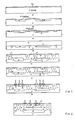
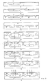
- a N type epitaxial layer is then grown, isolation regions are defined, base and emitter regions are made by diffusion, contacts are opened and the related zones metallized, all in accordance with the stages illustrated in Fig.1 .
- PNP transistors so obtained have a low level of efficiency as regards current handling (due to high base resistivity), frequency response (base being too thick) and saturation voltages (due to high collector series resistance).
- the present invention enables to overcome these draw strictlybacks since PNP and NPN transistors are thereby realized with reduced collector series resistances and practically equal low-concentration collector thicknesses, ensuring this way an excellent dynamic performance without forgoing maximum operational voltage.
- two P+ type regions 2 and 3 are made in the normal way, respectively forming the horizontal isolation region for the NPN transistor and the low-resistivity collector region for the PNP transistor.
- an N+ type region 4 is then formed serving as a low-resistivity collector region for the NPN transistor.
- An N type epitaxial layer 5 is than grown, namely one whose conductivity is of the same type as that of the substrate, as illustrated in Fig.5 .
- P+ type regions 6, 7, 8 and 9 are then diffused until they join with regions 2 and 3 ( Fig.6 ). It will be seen that regions 2, 6 and 7 taken together completely surround an N type region 10 within which the base and emitter regions of the NPN transistor will then be diffused, while regions 3, 8 and 9 all together act as a collector region for the PNP transistor.
- a P type region 12 is diffused to act as a low-concentration collector region for the PNP transistor.
- the base of said transistor is formed by known methods and is situated inside region 12: it is an N type region and is indicated by the number 13, Fig.7 .
- P+ type regions 14 and 15 are then made, respectively forming the base of the NPN transistor and the emitter of the PNP transistor, region 14 being realized in such a way to ensure a low-concentration collector thickness of transistor NPN (see thickness s1 of Fig.8) practically equal to the low-concentration collector thickness of transistor PNP (see thickness s2 of the same figure).
- regions 16, 17, 18, 19 are diffused,these being respectively the emitter of the NPN transistor and enrichments for the contact regions of the collector of the NPN transistor, of the base of the PNP transistor and of the N type isolation region formed by regions 1 and 5 together ( Fig.8 ).
- N type isolation region must be connected at the point of highest potential among all those present in the device in order to have the various components electrically insulated from each other.
- Fig.9 gives some typical profiles of doping concentration along a section of the NPN and PNP transistors made according to the invented process: the profiles represent the logarithm of concentration c (atoms/cm3) of dopant in relation to the depth p of some points on the section (the various regions touched by the section are indicated on the axis of the abscissa).
- the first of these two circumstances involves the presence of a considerable quantity of dopant in the isolation region 2 ensuring high punch-through voltages for this layer.
- the second is a necessary condition for get ting the above thicknesses equal.
- Boron the P type dopant impurity
- arsenic or antimony the N type dopant impurities which can be used to make region 4
- the surface concentration of layer 2 thus has to be lower than that of layer 4 (in the stage illustrated in Fig.5).
Landscapes
- Bipolar Integrated Circuits (AREA)
- Bipolar Transistors (AREA)
Applications Claiming Priority (2)
| Application Number | Priority Date | Filing Date | Title |
|---|---|---|---|
| IT2035788 | 1988-04-28 | ||
| IT20357/88A IT1218230B (it) | 1988-04-28 | 1988-04-28 | Procedimento per la formazione di un circuito integrato su un substrato di tipo n,comprendente transistori pnp e npn verticali e isolati fra loro |
Publications (2)
| Publication Number | Publication Date |
|---|---|
| EP0339732A1 true EP0339732A1 (de) | 1989-11-02 |
| EP0339732B1 EP0339732B1 (de) | 1993-10-27 |
Family
ID=11166004
Family Applications (1)
| Application Number | Title | Priority Date | Filing Date |
|---|---|---|---|
| EP89201041A Expired - Lifetime EP0339732B1 (de) | 1988-04-28 | 1989-04-24 | Verfahren zur Herstellung einer auf einem N-Typ-Substrat integrierten Schaltung, umfassend vertikale PNP- und NPN-Transistoren, die voneinander isoliert sind |
Country Status (5)
| Country | Link |
|---|---|
| US (1) | US4898836A (de) |
| EP (1) | EP0339732B1 (de) |
| JP (1) | JP2703798B2 (de) |
| DE (1) | DE68910169T2 (de) |
| IT (1) | IT1218230B (de) |
Cited By (8)
| Publication number | Priority date | Publication date | Assignee | Title |
|---|---|---|---|---|
| EP0439899A3 (en) * | 1990-01-25 | 1991-11-06 | Precision Monolithics Inc. | Complementary bipolar transistors compatible with cmos process |
| EP0476757A3 (en) * | 1990-09-19 | 1992-07-29 | Koninkl Philips Electronics Nv | A method of manufacturing a semiconductor device |
| EP0509183A1 (de) * | 1986-10-01 | 1992-10-21 | Consorzio per la Ricerca sulla Microelettronica nel Mezzogiorno - CoRiMMe | Monolitische Halbleiteranordnung bestehend aus einer integrierten Kontrollschaltung und aus mindestens einem Leistungstransistor, die auf demselben Chip integriert sind und Herstellungsverfahren |
| US5597742A (en) * | 1991-04-17 | 1997-01-28 | Consorzio Per La Ricerca Sulla Microelettronica Nel Mezzogiorno | Semiconductor device and method |
| EP0756329A1 (de) | 1995-07-27 | 1997-01-29 | Consorzio per la Ricerca sulla Microelettronica nel Mezzogiorno - CoRiMMe | Vertikaler PNP-Transistor und Verfahren zur Herstellung |
| EP0792514A4 (de) * | 1994-11-04 | 1998-06-17 | Analog Devices Inc | Integrierter schaltkreis mit komplementären isolierten bipolartransistoren und dessen herstellungsverfahren |
| EP0915508A1 (de) * | 1997-10-10 | 1999-05-12 | STMicroelectronics S.r.l. | Integrierte Schaltung mit hocheffizienter Isolation durch PN-Übergang |
| EP1453104A3 (de) * | 2003-02-28 | 2005-06-01 | Texas Instruments Inc. | Vertikaler Bipolartransistor und Verfahren zur Herstellung |
Families Citing this family (12)
| Publication number | Priority date | Publication date | Assignee | Title |
|---|---|---|---|---|
| USRE35642E (en) * | 1987-12-22 | 1997-10-28 | Sgs-Thomson Microelectronics, S.R.L. | Integrated high-voltage bipolar power transistor and low voltage MOS power transistor structure in the emitter switching configuration and relative manufacturing process |
| IT1217323B (it) * | 1987-12-22 | 1990-03-22 | Sgs Microelettronica Spa | Struttura integrata di transistor bipolare di potenza di alta tensione e di transistor mos di potenza di bassa tensione nella configurazione"emitter switching"e relativo processo di fabbricazione |
| US5156989A (en) * | 1988-11-08 | 1992-10-20 | Siliconix, Incorporated | Complementary, isolated DMOS IC technology |
| US5286986A (en) * | 1989-04-13 | 1994-02-15 | Kabushiki Kaisha Toshiba | Semiconductor device having CCD and its peripheral bipolar transistors |
| JPH07105458B2 (ja) * | 1989-11-21 | 1995-11-13 | 株式会社東芝 | 複合型集積回路素子 |
| JP2748988B2 (ja) * | 1991-03-13 | 1998-05-13 | 三菱電機株式会社 | 半導体装置とその製造方法 |
| EP0555496B1 (de) * | 1991-07-03 | 1997-03-26 | Consorzio per la Ricerca sulla Microelettronica nel Mezzogiorno - CoRiMMe | Laterale Bipolartransistorstruktur mit integriertem Kontrollschaltkreis und integriertem Leistungstransistor und deren Herstellungsprozess |
| US5702959A (en) * | 1995-05-31 | 1997-12-30 | Texas Instruments Incorporated | Method for making an isolated vertical transistor |
| JP3409548B2 (ja) * | 1995-12-12 | 2003-05-26 | ソニー株式会社 | 半導体装置の製造方法 |
| EP0809294B1 (de) * | 1996-05-21 | 2002-01-02 | Co.Ri.M.Me. Consorzio Per La Ricerca Sulla Microelettronica Nel Mezzogiorno | Leistungshalbleiterbauelementstruktur mit vertikalem PNP-Transistor |
| JP3529549B2 (ja) | 1996-05-23 | 2004-05-24 | 東芝マイクロエレクトロニクス株式会社 | 半導体装置の製造方法 |
| JPH104142A (ja) * | 1996-06-18 | 1998-01-06 | Sony Corp | 半導体装置の製造方法 |
Citations (2)
| Publication number | Priority date | Publication date | Assignee | Title |
|---|---|---|---|---|
| GB1193692A (en) * | 1966-12-13 | 1970-06-03 | Texas Instruments Inc | Process for Fabricating Integrated Circuits |
| FR2095386A1 (de) * | 1970-06-20 | 1972-02-11 | Philips Nv |
Family Cites Families (11)
| Publication number | Priority date | Publication date | Assignee | Title |
|---|---|---|---|---|
| US3079287A (en) * | 1959-09-01 | 1963-02-26 | Texas Instruments Inc | Improved grown junction transistor and method of making same |
| NL145396B (nl) * | 1966-10-21 | 1975-03-17 | Philips Nv | Werkwijze ter vervaardiging van een geintegreerde halfgeleiderinrichting en geintegreerde halfgeleiderinrichting, vervaardigd volgens de werkwijze. |
| US3930909A (en) * | 1966-10-21 | 1976-01-06 | U.S. Philips Corporation | Method of manufacturing a semiconductor device utilizing simultaneous outdiffusion during epitaxial growth |
| US4054899A (en) * | 1970-09-03 | 1977-10-18 | Texas Instruments Incorporated | Process for fabricating monolithic circuits having matched complementary transistors and product |
| US3793088A (en) * | 1972-11-15 | 1974-02-19 | Bell Telephone Labor Inc | Compatible pnp and npn devices in an integrated circuit |
| US4038680A (en) * | 1972-12-29 | 1977-07-26 | Sony Corporation | Semiconductor integrated circuit device |
| DE2351985A1 (de) * | 1973-10-17 | 1975-04-30 | Itt Ind Gmbh Deutsche | Planardiffusionsverfahren zum herstellen einer monolithisch integrierten festkoerperschaltung |
| US3971059A (en) * | 1974-09-23 | 1976-07-20 | National Semiconductor Corporation | Complementary bipolar transistors having collector diffused isolation |
| JPS54136281A (en) * | 1978-04-14 | 1979-10-23 | Toko Inc | Semiconductor device and method of fabricating same |
| EP0093304B1 (de) * | 1982-04-19 | 1986-01-15 | Matsushita Electric Industrial Co., Ltd. | Integrierte Halbleiterschaltung und Verfahren zur Herstellung derselben |
| JPS59194465A (ja) * | 1983-04-19 | 1984-11-05 | Sanken Electric Co Ltd | 半導体集積回路の製造方法 |
-
1988
- 1988-04-28 IT IT20357/88A patent/IT1218230B/it active
-
1989
- 1989-04-21 US US07/341,540 patent/US4898836A/en not_active Expired - Lifetime
- 1989-04-24 EP EP89201041A patent/EP0339732B1/de not_active Expired - Lifetime
- 1989-04-24 DE DE89201041T patent/DE68910169T2/de not_active Expired - Fee Related
- 1989-04-27 JP JP1106088A patent/JP2703798B2/ja not_active Expired - Fee Related
Patent Citations (2)
| Publication number | Priority date | Publication date | Assignee | Title |
|---|---|---|---|---|
| GB1193692A (en) * | 1966-12-13 | 1970-06-03 | Texas Instruments Inc | Process for Fabricating Integrated Circuits |
| FR2095386A1 (de) * | 1970-06-20 | 1972-02-11 | Philips Nv |
Non-Patent Citations (3)
| Title |
|---|
| IBM TECHNICAL DISCLOSURE BULLETIN, vol. 16, no. 6, November 1973, pages 1707-1708, New York, US; I. ANTIPOV et al.: "Fabricating complementary semiconductor devices" * |
| IBM TECHNICAL DISCLOSURE BULLETIN, vol. 17, no. 1, June 1974, pages 21-22, New York, US; J.J: CHANG et al.: "Complementary bipolar device structure" * |
| PATENT ABSTRACTS OF JAPAN, vol. 9 no. 53 (E-301)[1776], 7th March 1985; & JP-A-59 194 465 (SANKEN DENKI K.K.) 05-11-1984 * |
Cited By (9)
| Publication number | Priority date | Publication date | Assignee | Title |
|---|---|---|---|---|
| EP0509183A1 (de) * | 1986-10-01 | 1992-10-21 | Consorzio per la Ricerca sulla Microelettronica nel Mezzogiorno - CoRiMMe | Monolitische Halbleiteranordnung bestehend aus einer integrierten Kontrollschaltung und aus mindestens einem Leistungstransistor, die auf demselben Chip integriert sind und Herstellungsverfahren |
| EP0439899A3 (en) * | 1990-01-25 | 1991-11-06 | Precision Monolithics Inc. | Complementary bipolar transistors compatible with cmos process |
| EP0476757A3 (en) * | 1990-09-19 | 1992-07-29 | Koninkl Philips Electronics Nv | A method of manufacturing a semiconductor device |
| US5597742A (en) * | 1991-04-17 | 1997-01-28 | Consorzio Per La Ricerca Sulla Microelettronica Nel Mezzogiorno | Semiconductor device and method |
| EP0792514A4 (de) * | 1994-11-04 | 1998-06-17 | Analog Devices Inc | Integrierter schaltkreis mit komplementären isolierten bipolartransistoren und dessen herstellungsverfahren |
| EP0756329A1 (de) | 1995-07-27 | 1997-01-29 | Consorzio per la Ricerca sulla Microelettronica nel Mezzogiorno - CoRiMMe | Vertikaler PNP-Transistor und Verfahren zur Herstellung |
| US6114746A (en) * | 1995-07-27 | 2000-09-05 | Consorzio Per La Ricerca Sullla Microelettronica Nel Mezzogiorno | Vertical PNP transistor and relative fabrication method |
| EP0915508A1 (de) * | 1997-10-10 | 1999-05-12 | STMicroelectronics S.r.l. | Integrierte Schaltung mit hocheffizienter Isolation durch PN-Übergang |
| EP1453104A3 (de) * | 2003-02-28 | 2005-06-01 | Texas Instruments Inc. | Vertikaler Bipolartransistor und Verfahren zur Herstellung |
Also Published As
| Publication number | Publication date |
|---|---|
| JPH0212926A (ja) | 1990-01-17 |
| US4898836A (en) | 1990-02-06 |
| IT1218230B (it) | 1990-04-12 |
| IT8820357A0 (it) | 1988-04-28 |
| DE68910169D1 (de) | 1993-12-02 |
| EP0339732B1 (de) | 1993-10-27 |
| DE68910169T2 (de) | 1994-04-07 |
| JP2703798B2 (ja) | 1998-01-26 |
Similar Documents
| Publication | Publication Date | Title |
|---|---|---|
| EP0339732A1 (de) | Verfahren zur Herstellung einer auf einem N-Typ-Substrat integrierten Schaltung, umfassend vertikale PNP- und NPN-Transistoren, die voneinander isoliert sind | |
| US4120707A (en) | Process of fabricating junction isolated IGFET and bipolar transistor integrated circuit by diffusion | |
| US3502951A (en) | Monolithic complementary semiconductor device | |
| US4047217A (en) | High-gain, high-voltage transistor for linear integrated circuits | |
| US4283236A (en) | Method of fabricating lateral PNP transistors utilizing selective diffusion and counter doping | |
| US4066473A (en) | Method of fabricating high-gain transistors | |
| EP0093304A1 (de) | Integrierte Halbleiterschaltung und Verfahren zur Herstellung derselben | |
| US4492008A (en) | Methods for making high performance lateral bipolar transistors | |
| EP0262723A2 (de) | Verfahren zur Herstellung einer monolithischen Hochspannungshalbleiterschaltung | |
| US4137109A (en) | Selective diffusion and etching method for isolation of integrated logic circuit | |
| US4210925A (en) | I2 L Integrated circuit and process of fabrication | |
| US4054899A (en) | Process for fabricating monolithic circuits having matched complementary transistors and product | |
| EP0429834A1 (de) | Bipolartransistorstruktur mit erhobener Basis und deren Herstellungsverfahren | |
| US4255209A (en) | Process of fabricating an improved I2 L integrated circuit utilizing diffusion and epitaxial deposition | |
| EP0051534B1 (de) | Selbstjustierendes Verfahren zur Herstellung integrierter Stromkreisstrukturen unter Verwendung unterschiedlicher Oxydationsraten | |
| US3770519A (en) | Isolation diffusion method for making reduced beta transistor or diodes | |
| US5837590A (en) | Isolated vertical PNP transistor without required buried layer | |
| EP0328286B1 (de) | Verfahren zur Herstellung eines vertikalen PNP-Vielfachkollektortransistors | |
| US4550491A (en) | Method of making substrate injection logic operator structure | |
| US5302848A (en) | Integrated circuit with complementary junction-isolated bipolar transistors | |
| US5481132A (en) | Transistor with a predetermined current gain in a bipolar integrated circuit | |
| US3968511A (en) | Semiconductor device with additional carrier injecting junction adjacent emitter region | |
| US4140559A (en) | Method of fabricating an improved substrate fed logic utilizing graded epitaxial deposition | |
| US5529939A (en) | Method of making an integrated circuit with complementary isolated bipolar transistors | |
| US3761326A (en) | Process for making an optimum high gain bandwidth phototransistor structure |
Legal Events
| Date | Code | Title | Description |
|---|---|---|---|
| PUAI | Public reference made under article 153(3) epc to a published international application that has entered the european phase |
Free format text: ORIGINAL CODE: 0009012 |
|
| AK | Designated contracting states |
Kind code of ref document: A1 Designated state(s): DE FR GB NL |
|
| 17P | Request for examination filed |
Effective date: 19900320 |
|
| 17Q | First examination report despatched |
Effective date: 19920709 |
|
| GRAA | (expected) grant |
Free format text: ORIGINAL CODE: 0009210 |
|
| AK | Designated contracting states |
Kind code of ref document: B1 Designated state(s): DE FR GB NL |
|
| PG25 | Lapsed in a contracting state [announced via postgrant information from national office to epo] |
Ref country code: NL Effective date: 19931027 |
|
| REF | Corresponds to: |
Ref document number: 68910169 Country of ref document: DE Date of ref document: 19931202 |
|
| ET | Fr: translation filed | ||
| NLV1 | Nl: lapsed or annulled due to failure to fulfill the requirements of art. 29p and 29m of the patents act | ||
| PLBE | No opposition filed within time limit |
Free format text: ORIGINAL CODE: 0009261 |
|
| STAA | Information on the status of an ep patent application or granted ep patent |
Free format text: STATUS: NO OPPOSITION FILED WITHIN TIME LIMIT |
|
| 26N | No opposition filed | ||
| REG | Reference to a national code |
Ref country code: FR Ref legal event code: D6 |
|
| REG | Reference to a national code |
Ref country code: GB Ref legal event code: IF02 |
|
| PGFP | Annual fee paid to national office [announced via postgrant information from national office to epo] |
Ref country code: FR Payment date: 20020410 Year of fee payment: 14 |
|
| PGFP | Annual fee paid to national office [announced via postgrant information from national office to epo] |
Ref country code: GB Payment date: 20020424 Year of fee payment: 14 |
|
| PGFP | Annual fee paid to national office [announced via postgrant information from national office to epo] |
Ref country code: DE Payment date: 20020502 Year of fee payment: 14 |
|
| PG25 | Lapsed in a contracting state [announced via postgrant information from national office to epo] |
Ref country code: GB Free format text: LAPSE BECAUSE OF NON-PAYMENT OF DUE FEES Effective date: 20030424 |
|
| PG25 | Lapsed in a contracting state [announced via postgrant information from national office to epo] |
Ref country code: DE Free format text: LAPSE BECAUSE OF NON-PAYMENT OF DUE FEES Effective date: 20031101 |
|
| GBPC | Gb: european patent ceased through non-payment of renewal fee | ||
| PG25 | Lapsed in a contracting state [announced via postgrant information from national office to epo] |
Ref country code: FR Free format text: LAPSE BECAUSE OF NON-PAYMENT OF DUE FEES Effective date: 20031231 |
|
| REG | Reference to a national code |
Ref country code: FR Ref legal event code: ST |