EP0340725A2 - ECL/TTL-Pegelumsetzungsschaltung - Google Patents
ECL/TTL-Pegelumsetzungsschaltung Download PDFInfo
- Publication number
- EP0340725A2 EP0340725A2 EP89107934A EP89107934A EP0340725A2 EP 0340725 A2 EP0340725 A2 EP 0340725A2 EP 89107934 A EP89107934 A EP 89107934A EP 89107934 A EP89107934 A EP 89107934A EP 0340725 A2 EP0340725 A2 EP 0340725A2
- Authority
- EP
- European Patent Office
- Prior art keywords
- transistor
- collector
- emitter
- base
- resistor
- Prior art date
- Legal status (The legal status is an assumption and is not a legal conclusion. Google has not performed a legal analysis and makes no representation as to the accuracy of the status listed.)
- Withdrawn
Links
- 230000003071 parasitic effect Effects 0.000 description 8
- 238000010586 diagram Methods 0.000 description 6
- 230000003247 decreasing effect Effects 0.000 description 3
- 230000002411 adverse Effects 0.000 description 2
- 230000004888 barrier function Effects 0.000 description 1
- 238000010276 construction Methods 0.000 description 1
- 230000007547 defect Effects 0.000 description 1
- 230000004048 modification Effects 0.000 description 1
- 238000012986 modification Methods 0.000 description 1
- 230000001131 transforming effect Effects 0.000 description 1
Images

Classifications
-
- H—ELECTRICITY
- H03—ELECTRONIC CIRCUITRY
- H03K—PULSE TECHNIQUE
- H03K19/00—Logic circuits, i.e. having at least two inputs acting on one output; Inverting circuits
- H03K19/0175—Coupling arrangements; Interface arrangements
- H03K19/018—Coupling arrangements; Interface arrangements using bipolar transistors only
- H03K19/01806—Interface arrangements
- H03K19/01812—Interface arrangements with at least one differential stage
Definitions
- the present invention relates to an ECL-TTL level converting circuit, and more specifically to an ECL-TTL level converting circuit capable of preventing an increase of a low level potential due to parasitic resistance components of a package and the like.
- ECL-TTL level converting circuits have been widely used in conventional logic circuits for the purpose of interfacing between an ECL (emitter coupled logic) circuit and a TTL (transistor transistor logic) circuit.
- ECL emitter coupled logic
- TTL transistor transistor logic
- most of the conventional ECL-TTL circuits have such a circuit construction that when a low level signal of a TTL level is outputted, a maximum current is flowed into a ground. Therefore, a ground level will be increased by parasitic resistance components of a package and a ground line wiring of a voltage supply, with the result that a potential of the low level output signal will be adversely increased.
- Another object of the present invention is to provide an ECL-TTL level converting circuit capable of outputting of a low level signal having a stable potential which is not remarkably influenced by parasitic resistance components of a package and the like.
- an ECL-TTL level converting circuit comprising a first transistor having a collector connected to a ground line and an emitter connected to a negative voltage line through a constant current source, a second transistor having a collector connected to a positive voltage line through a first resistor and an emitter commonly connected to the emitter of the first transistor, the base of one of the first and second transistors being connected to receive a reference voltage and the base of the other of the first and second transistors being connected to receive an input signal, a third transistor having a collector connected to the positive voltage line through a second resistor, an emitter connected to the ground line through a third resistor and a base connected to the collector of the second transistor so that the collector of the third transistor outputs a first drive signal and the emitter of the third transistor outputs a second drive signal, an amplifying stage having an input connected to the collector of the third transistor, and a fourth transistor having a collector connected to an output side of the amplifying stage,
- each of the third and fourth transistors is a Schottky diode transistor.
- the amplifying stage is composed of a fifth transistor having a collector connected to the positive voltage line through a fourth resistor, a base connected to the collector of the third transistor and an emitter connected to the collector of the fourth transistor through a diode which is connected in a forward direction from the emitter of the fifth transistor to the collector of the fourth transistor.
- ECL-TTL level converting circuit includes an emitter-coupled type differential amplifying circuit operating between a ground level GND and a negative electric supply voltage V EE , and a TTL "totem pole" type output circuit operating between the ground level GND and a positive electric supply voltage V CC .
- the emitter-coupled type differential amplifying circuit includes a pair of transistors Q11 and Q12 having their commonly connected emitters which are connected through a constant current source I CS to the ground GND.
- a base of the transistor Q11 is connected to an input terminal IN so as to receive an input signal of an ECL level, and a base of the transistor Q12 is connected to receive a reference voltage V ref .
- a collector of the transistor Q11 is connected to one end of a resistor R11, which is in turn connected at its other end to the positive voltage line V CC .
- a bias circuit composed of a resistors R12 and R13 and diodes D11 and D12 connected in series between the positive voltage line V CC and the ground GND in the named order and in a forward direction.
- a transistor Q13 is connected at its collector to the positive voltage V CC , and at its base to a connection node between the resistors R12 and R13.
- the collector of the transistor Q11 is also connected to a base of an off-buffer side output transistor Q14.
- a collector of the transistor Q12 is connected to an emitter of the transistor Q13 through a resistor R14 and a base of an on-buffer side output transistor Q15, which is in turn connected between an output terminal OUT and the ground GND.
- the transistor Q15 is a so-called Schottky diode transistor which includes therein an integrated Schottky barrier diode in parallel with the base-collector junction.
- a collector of the transistor Q14 is connected through a resistor R15 to the positive voltage line V CC , and an emitter of the transistor Q14 is connected through a diode D13 to the collector of the transistor Q15.
- ECL-TTL level converting circuit operates as follows:
- the transistor Q14 If a low level signal is supplied to the input terminal IN, the transistor Q14 is turned on so that a current flow through the diode D13. However, the transistor Q15 is turned off. Therefore, a high level signal of the TTL level is generated from the output terminal OUT.
- V OL is a TTL output voltage of the low level
- V F(Q14) is a base-emitter voltage of the transistor Q14 in the on condition
- V F(D13) is a forward direction voltage of the diode D13 in the on condition.
- the base potential of the transistor Q15 is a value by transforming the bias voltage generated by the base bias circuit (the series circuit of the resistors R12 and R13 and the diodes D11 and D12 between the positive voltage Vcc and the ground GND) by means of an emitter follower composed of the transistor Q13 and the resistor R14.
- V F(D11) , V F(D12) is a forward direction voltage of the diodes D11 and D12
- V F(Q15) is a base-emitter voltage of the transistor Q15 in the on condition
- V F(Q13) is a base-emitter voltage of the transistor Q13 when the constant current Ics flows through the transistor Q13.
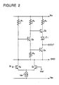
- the shown ECL-TTL level converting circuit includes a first transistor Q1 having a collector connected to a ground line GND and an emitter connected to a negative voltage line V EE through a constant current source I CS .
- a base of the first transistor Q1 is connected to receive a reference voltage V ref .
- a second transistor Q2 is connected at its collector to a positive voltage line V CC through a first resistor R1.
- An emitter of the second transistor Q2 is commonly connected to the emitter of the first transistor Q1, and a base of the second transistor Q2 is connected to an input terminal IN so as to receive an input signal.
- the collector of the second transistor Q2 is also connected to a base of third transistor Q3, which is constituted of a Schottky diode transistor and is connected at its collector to the positive voltage line V CC through a second resistor R2.
- An emitter of the third transistor Q3 is connected to the ground line GND through a third resistor R3 and also connected to a base of a fourth transistor Q4.
- This fourth transistor Q4 forms an on-buffer side transistor, and is constituted of a Schottky diode transistor and having an emitter connected to the ground line GND.
- the collector of the third transistor Q3 is also connected to a base of a fifth transistor Q5 having a collector connected to the positive voltage line V CC through a fourth resistor R4, and an emitter connected to a collector of the fourth transistor Q4 through a diode D1 which is connected in a forward direction from the emitter of the fifth transistor Q5 to the collector of the fourth transistor Q4.
- the fifth transistor Q5 forms an off-buffer side transistor.
- the transistor Q1 When the ECL level input signal appearing on the input terminal IN is a low level, the transistor Q1 is turned on and the transistor Q2 is turned off. Therefore, the constant current I CS will flow from the ground GND through the transistor Q1 to the negative voltage V EE , and on the other hand, the transistor Q3 functioning as a phase division stage is brought into an on condition. Namely, since an electric current flows through the the transistor Q3, each of the resistors R2 and R3 generates a predetermined amount of voltage shift. In accordance with the respective voltage shift amounts of the resistors R2 and R3, the transistor Q4 is turned on and the transistor Q5 is turned off. Namely, a TTL low level signal is generated at the output terminal OUT.
- an electric current flowing to the ground GND includes an output terminal current I OL , a base current I B(Q4) of the transistor Q4, and a current I1 which generates across the resistor R3 a potential shift causing the transistor Q4 to turn on.
- an electric current flowing from the ground GND includes the constant current I CS since the transistor Q1 is in the on condition.
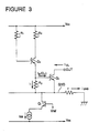
- the transistor Q4 when the TTL low level signal is outputted, the transistor Q4 is in the on condition so that a load current flows from the output terminal OUT through the transistor Q4 to the ground GND. However, at this time, since the transistor Q2 is in the on condition to allow the constant current I CS to flow out of the ground GND to the negative voltage V EE . In other words, not only a current flows into the ground, but also a current flows out of the ground. Therefore, the ground line current of the electric supply (through the resistor "r" in Figure 3) can be equivalently decreased, and accordingly, the potential increase of the ground level caused due to the parasitic resistance components "r" is effectively prevented. Thus, the increase of the TTL low level can be prevented.
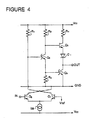
- the ECL-TTL level converting circuit shown in Figure 2 can be modified as shown in Figure 4. Namely, the collector of the transistor Q1 is connected to the resister R1 and the collector of the transistor Q2 is connected to the ground GND. Accordingly, the circuit shown in Figure 4 constitutes an inverter circuit which generates, at the output OUT, a TTL output signal in a phase opposite to that of the input ECL signal appearing on the input IN.
- the ECL-TTL level converting circuit in accordance with the present invention, a portion of the load current flowing through the output terminal to the ground is flowed out or discharged from the ground to the negative voltage through intermediary of the differential circuit, regardless of the non-inverting type or the inverting type. Therefore, the ground line current of the electric supply can be equivalently decreased, and accordingly, the increase of the ground potential caused due to the parasitic resistance components of the package and the ground line wiring of the electric supply is effectively prevented.
- the ECL-TTL level converting circuit in accordance with the present invention can effectively prevent the increase of the TTL low level signal, regardless of the non-inverting type or the inverting type.
Landscapes
- Engineering & Computer Science (AREA)
- Computer Hardware Design (AREA)
- Physics & Mathematics (AREA)
- Computing Systems (AREA)
- General Engineering & Computer Science (AREA)
- Mathematical Physics (AREA)
- Logic Circuits (AREA)
Applications Claiming Priority (2)
| Application Number | Priority Date | Filing Date | Title |
|---|---|---|---|
| JP109665/88 | 1988-05-02 | ||
| JP63109665A JPH01279633A (ja) | 1988-05-02 | 1988-05-02 | Ecl−ttlレベル変換回路 |
Publications (2)
| Publication Number | Publication Date |
|---|---|
| EP0340725A2 true EP0340725A2 (de) | 1989-11-08 |
| EP0340725A3 EP0340725A3 (de) | 1990-08-08 |
Family
ID=14516061
Family Applications (1)
| Application Number | Title | Priority Date | Filing Date |
|---|---|---|---|
| EP89107934A Withdrawn EP0340725A3 (de) | 1988-05-02 | 1989-05-02 | ECL/TTL-Pegelumsetzungsschaltung |
Country Status (3)
| Country | Link |
|---|---|
| US (1) | US5065051A (de) |
| EP (1) | EP0340725A3 (de) |
| JP (1) | JPH01279633A (de) |
Cited By (1)
| Publication number | Priority date | Publication date | Assignee | Title |
|---|---|---|---|---|
| EP0440192A1 (de) * | 1990-01-31 | 1991-08-07 | Kabushiki Kaisha Toshiba | ECL-Schaltung in einem integrierten Halbleiterschaltkreis |
Families Citing this family (1)
| Publication number | Priority date | Publication date | Assignee | Title |
|---|---|---|---|---|
| US9054695B2 (en) * | 2013-10-01 | 2015-06-09 | Texas Instruments Incorporated | Technique to realize high voltage IO driver in a low voltage BiCMOS process |
Family Cites Families (8)
| Publication number | Priority date | Publication date | Assignee | Title |
|---|---|---|---|---|
| JPS59181724A (ja) * | 1983-03-31 | 1984-10-16 | Fujitsu Ltd | ゲ−トアレイlsi装置 |
| US4684831A (en) * | 1984-08-21 | 1987-08-04 | Applied Micro Circuits Corporation | Level shift circuit for interfacing between two different voltage levels using a current mirror circuit |
| EP0216756B1 (de) * | 1984-11-02 | 1990-03-07 | Advanced Micro Devices, Inc. | Integrierte schaltungsvorrichtung, die eingangssignale annimmt und ausgangssignale erzeugt auf den höhen verschiedener logischer scharen |
| US4677320A (en) * | 1985-05-02 | 1987-06-30 | Fairchild Semiconductor Corporation | Emitter coupled logic to transistor transistor logic translator |
| US4644194A (en) * | 1985-06-24 | 1987-02-17 | Motorola, Inc. | ECL to TTL voltage level translator |
| EP0250007A3 (de) * | 1986-06-19 | 1989-12-27 | Advanced Micro Devices, Inc. | TTL-Pufferschaltung |
| JP2538612B2 (ja) * | 1987-09-18 | 1996-09-25 | 富士通株式会社 | Ecl/ttlレベル変換回路 |
| JPH0683053B2 (ja) * | 1987-10-30 | 1994-10-19 | 日本電気株式会社 | レベル変換回路 |
-
1988
- 1988-05-02 JP JP63109665A patent/JPH01279633A/ja active Pending
-
1989
- 1989-05-02 EP EP89107934A patent/EP0340725A3/de not_active Withdrawn
- 1989-05-02 US US07/346,160 patent/US5065051A/en not_active Expired - Fee Related
Cited By (2)
| Publication number | Priority date | Publication date | Assignee | Title |
|---|---|---|---|---|
| EP0440192A1 (de) * | 1990-01-31 | 1991-08-07 | Kabushiki Kaisha Toshiba | ECL-Schaltung in einem integrierten Halbleiterschaltkreis |
| US5122683A (en) * | 1990-01-31 | 1992-06-16 | Kabushiki Kaisha Toshiba | Ecl circuit with feedback controlled pull down in output |
Also Published As
| Publication number | Publication date |
|---|---|
| US5065051A (en) | 1991-11-12 |
| JPH01279633A (ja) | 1989-11-09 |
| EP0340725A3 (de) | 1990-08-08 |
Similar Documents
| Publication | Publication Date | Title |
|---|---|---|
| US4629913A (en) | Circuit arrangement for converting ECL-logic signals to TTL-logic signals | |
| WO1985002955A1 (en) | Transient active pull-down | |
| EP0219937A2 (de) | Gesteuerter ECL-Referenzgenerator | |
| JPS62230222A (ja) | 入力回路 | |
| US5065051A (en) | Ecl-ttl level converting circuit | |
| EP0098155B1 (de) | Schmitt-Trigger-Schaltung | |
| US4977339A (en) | Semiconductor integrated circuit having a MOS transistor with a threshold level to enable a level conversion | |
| EP0435335B1 (de) | Transistorschaltung und Pegelkonverterschaltung | |
| JPS61293022A (ja) | Ecl−ttl変換出力回路 | |
| JP2699823B2 (ja) | 半導体集積回路 | |
| US5349287A (en) | Low power comparator having a non-saturating current mirror load | |
| EP0366294A2 (de) | TTL-ECL-Pegelumsetzungsschaltung | |
| US4967106A (en) | Emitter-coupled logic circuit | |
| JP3507621B2 (ja) | 半導体集積回路 | |
| US5233234A (en) | Emitter follower output circuit | |
| US20010013794A1 (en) | Buffer circuit | |
| JPH0575438A (ja) | 相補型エミツタフオロワ | |
| EP0054408A1 (de) | Logikschaltung | |
| JP3233473B2 (ja) | 電圧レベル変換回路 | |
| KR910010876A (ko) | Ecl회로를 갖는 반도체 집적회로 | |
| JP2998368B2 (ja) | Ttl論理回路 | |
| JP2827743B2 (ja) | 半導体集積回路装置 | |
| JP2814843B2 (ja) | 差動増幅器 | |
| JPH03293813A (ja) | 半導体集積回路 | |
| JPS6315527A (ja) | 論理回路 |
Legal Events
| Date | Code | Title | Description |
|---|---|---|---|
| PUAI | Public reference made under article 153(3) epc to a published international application that has entered the european phase |
Free format text: ORIGINAL CODE: 0009012 |
|
| 17P | Request for examination filed |
Effective date: 19890502 |
|
| AK | Designated contracting states |
Kind code of ref document: A2 Designated state(s): DE FR GB |
|
| PUAL | Search report despatched |
Free format text: ORIGINAL CODE: 0009013 |
|
| AK | Designated contracting states |
Kind code of ref document: A3 Designated state(s): DE FR GB |
|
| 17Q | First examination report despatched |
Effective date: 19920306 |
|
| STAA | Information on the status of an ep patent application or granted ep patent |
Free format text: STATUS: THE APPLICATION HAS BEEN WITHDRAWN |
|
| 18W | Application withdrawn |
Withdrawal date: 19920424 |