EP0340895A2 - Test de circuit logique et de mémoire - Google Patents
Test de circuit logique et de mémoire Download PDFInfo
- Publication number
- EP0340895A2 EP0340895A2 EP89302304A EP89302304A EP0340895A2 EP 0340895 A2 EP0340895 A2 EP 0340895A2 EP 89302304 A EP89302304 A EP 89302304A EP 89302304 A EP89302304 A EP 89302304A EP 0340895 A2 EP0340895 A2 EP 0340895A2
- Authority
- EP
- European Patent Office
- Prior art keywords
- data
- pattern generator
- random pattern
- memory
- circuits
- Prior art date
- Legal status (The legal status is an assumption and is not a legal conclusion. Google has not performed a legal analysis and makes no representation as to the accuracy of the status listed.)
- Withdrawn
Links
Images
Classifications
-
- G—PHYSICS
- G11—INFORMATION STORAGE
- G11C—STATIC STORES
- G11C29/00—Checking stores for correct operation ; Subsequent repair; Testing stores during standby or offline operation
- G11C29/04—Detection or location of defective memory elements, e.g. cell constructio details, timing of test signals
- G11C29/08—Functional testing, e.g. testing during refresh, power-on self testing [POST] or distributed testing
- G11C29/12—Built-in arrangements for testing, e.g. built-in self testing [BIST] or interconnection details
- G11C29/18—Address generation devices; Devices for accessing memories, e.g. details of addressing circuits
- G11C29/20—Address generation devices; Devices for accessing memories, e.g. details of addressing circuits using counters or linear-feedback shift registers [LFSR]
-
- G—PHYSICS
- G11—INFORMATION STORAGE
- G11C—STATIC STORES
- G11C29/00—Checking stores for correct operation ; Subsequent repair; Testing stores during standby or offline operation
- G11C29/04—Detection or location of defective memory elements, e.g. cell constructio details, timing of test signals
- G11C29/08—Functional testing, e.g. testing during refresh, power-on self testing [POST] or distributed testing
- G11C29/12—Built-in arrangements for testing, e.g. built-in self testing [BIST] or interconnection details
- G11C29/36—Data generation devices, e.g. data inverters
Definitions
- This invention relates to a system and method for high-efficiency memory circuit testing. More particularly, the invention is an on-chip system and method for performing self-test of either or both logic and memory circuits.
- a black box technique is used.
- a circuit is provided with a deterministic stimulus, thereby generating a response from the circuit, which is compared to a known expected output. Based on the comparisons, the circuit is determined to be simply good or bad.
- Past problems with the testing of integrated circuitry are the large test data volumes and long test times.
- Self-test refers to the presence of testing circuits which are on a component containing the circuits to be tested.
- the component may be a card, wafer, or an integrated circuit chip.
- self-test may be accomplished with testing circuits integrated into the circuits to be tested (i.e., on-chip), or located externally on the component (i.e., off-chip).
- on-chip testing is advantageous because the testing circuits need not be reproduced with the production of each integrated circuit chip.
- On-chip testing is considered advantageous because of its closeness to the circuits being tested, thereby making testing available at significantly higher speeds than for off-chip testing and requiring little more than an external power supply. In recent years, the balance has swung in favour of on-chip testing because the increase in integrated circuit density available has reduced the emphasis on chip real estate and increased the emphasis on testing speed.
- On-chip circuit testing can be divided into areas of logic circuit testing and memory circuit testing. For both types of on-chip testing it is desirable to be able to test all storage points in both the logical zero and one states. Due to recent increases in on-chip circuit density, it is becoming more likely that integrated circuit chips will contain both logic and memory circuits. Thus, there is an increasing need to be able to test both logic circuits and memory circuits on the same chip. However, most known circuit testing techniques are directed merely to the testing of logic circuits.
- the problem presented by the testing of logic circuits is the accessibility and observability of the logic circuit storage elements (latches). These storage elements are typically interconnected in such a manner that data cannot be inputted into a particular logic circuit storage element independently of other storage elements. Control of the independent logic circuit storage elements is required for logic circuit testing so that a known stimulus can be provided to the logic circuits, and the results can be observed.
- LSSD level sensitive scan design
- LSSD testing is implemented by imparting a shift register capability to each of the logic system latches and by making these shift register latches (SRL's) accessible during an input/output mode.
- LSSD testing requires operation of the logic circuits in two separate modes. In the first mode, known test data is serially inputted and shifted to the appropriate SRL locations. With the SRL initialized to a known state, operation of the logic circuits in the second mode begins. Known test data is thus propagated through the logic circuits to act as a stimuli to the system, the results being captured in the SRL's. Upon reversion to the original mode of operation, the status of the SRL's can be outputted and compared with known data which would be present if the circuitry operated correctly.
- SRL's shift register latches
- the advantage of signature analysis over simple deterministic testing is the compression of the outputted test data.
- the storing of test data for each output response is no longer required, thereby reducing tester complexity and test data volume.
- this feature also prevents the ability to easily determine the precise location of a circuit failure, such is irrelevant because the high circuit density and low cost of integrated circuit chips has made it impractical to repair a detected failure. Instead, a failed chip is discarded and another substituted in its place.
- a random pattern generator simply having the same number of stages as there are address lines required for memory addressing will not cycle through all memory addresses.
- the exclusive OR gate(s) in the feedback loop inevitably receive and therefore return a logical one to the initial stage of the shift register, thereby preventing the generation of the memory address consisting of all zeros. This is good in the sense that the presence of all zeros in the shift register would cause the random pattern generator to repeat the all zero state because the exclusive OR gate feedback loop would never generate anything but additional zeros. However, the all zero address must still be generated for complete testing. Thus, a simple system and method for generating the memory address consisting of all zeros is required.
- the output window is an array of data, the rows of which are formed from the data present in some of the stages of the shift register at various times during the data pattern.
- the array is generated inefficiently, using only a small portion of the existing stages of the shift register. This is because the proposal is directed to the generation of the all zero state in the entire array, not the generation of an all zero state in the shift register.
- the number of stages in the shift register do not correspond to the number of lines needed for addressing, and are reduced only by a complex logic circuit for inputting data from the shift register into the array. Furthermore, the complexity of the logic circuit makes it difficult to adapt to a particular memory size. Thus, no simple manner is heretofore known for providing a random pattern generator with the capability of cycling through all memory addresses.
- the object of this invention is accomplished using a random pattern generator (RPG) configuration including a linear feedback shift register containing at least one more stage than address lines needed for addressing the memory.
- the data from the additional RPG stages are not used in so far as memory addressing is concerned.
- the RPG design is based upon a primitive polynomial. Such a RPG ensures that cycling through all possible combinations of the test data patterns accounts for each memory address in the memory circuits, including the address of all zeros. The all-zero address is accounted for when the RPG generates all zeros, except for a one(s) in at least one of the additional stage(s) of the shift register.
- the RPG is first seeded with known test data, not all zeros, the multiple input signature register (MISR) with known data, and the memory data input shift register with the final N bits from the RPG as if the RPG had just finished a complete cycle using the intended seed.
- MISR multiple input signature register
- each memory address is generated and data written into that address, so that data is initialized into each memory cell.
- data from each memory cell is outputted to the MISR.
- the complement of the data initialized into memory during the first RPG cycle is written into memory.
- a final RPG cycle causes the complement data to be outputted to the MISR.
- the signature generated by the MISR is then compared to that known for a good memory array.
- the failure of a memory circuit element cannot be precisely located, such is irrelevant because the failure cannot practically be repaired on-chip. Instead, the failed chip is discarded and replaced.
- Logic testing uses the same RPG as for memory testing, employing LSSD techniques.
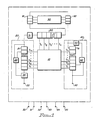
- Memory circuits 10 include an array of data words each containing "n" bits. Data is written into memory 10 via input lines I1, I2, I3 . . . I n and read out from memory 10 via output lines O1, O2, O3 . . . O n . Memory addressing during read/write operations is accomplished via "m" address lines A1, A2, A3 . . . A m . Memory 10 can therefore contain up to 2 m word lines and up to (2 m x n) memory cells. The testing circuits can thus be adapted for any size memory, the exact values of m and n being significant only as stated herein.
- Address data for memory 10 are generated by a random pattern generator (RPG) 20.
- Seed data can be entered into a shift register 21 of RPG 20 via an input node 22.
- Data bits from different stages of shift register 21 are inputted into exclusive OR gate 23, the output of which is rerouted as input data back into shift register 21 via multiplexer 24.
- RPG 20 is thus capable of cycling through a set of pseudo-random data patterns.
- pseudo-random it is meant that the data patterns are random only in so far as the selection of the seed data and the configuration of the feedback path of the RPG. Provided the same seed data are always used, the test patterns are repeatable.
- RPG 20 The design of RPG 20 is based upon a "primitive polynomial.”
- the stages of shift register 21 which are used to generate feedback to form the next state can be described by a polynomial.
- the feedback will be described by a zth degree polynomial.
- the remainder of the polynomial describes the feedback loop of the RPG. Feedback from the last stage of the shift register would be a "1" (x0), feedback from the next to last stage of the shift register would be an "x" (x1), and so on.
- a four stage shift register having feedback from the last two stages would be described by the polynomial "x4 + x + 1." If the zth degree characteristic polynomial p(x) is irreducible (i.e. cannot be factored) and if: then p(x) is a primitive polynomial. At least one primitive polynomial of degree z exists for every possible value of z. Examples of primitive polynomials are available in table form in various references. See, Peterson, W.W., and Weldon, E.J., Error Correcting Codes, 2nd Ed ., 1972.
- Sample primitive polynomials are x4 + x3 + 1, x5 + x2 + 1, x18 + x7 + 1, x21 + x2 + 1, and x31 + x3 +1.
- the actual configuration of RPG 20 may vary according to the size of shift register 21.
- a random pattern generator based on a primitive polynomial and having z stages will generate (2 z - 1) states if permitted to cycle through all possible data states. All data states are generated except for the all zero state. The all zero state cannot be generated because feedback from a data "1" in the shift register must inevitably regenerate another data "1". Thus only (2 z - 1) states can actually be generated. Note that shift register 21 contains at least one stage in addition to the number of address lines m (i.e., a total of at least (m + 1) stages, or z > m). Because of this feature, the all zero address of memory 10 can be generated.
- Shift register 30 has n stages connected to n input lines, permitting the input of words composed of n bits into memory 10. Data exiting the last stage of shift register 30 are routed through shift register 91. From shift register 91, data will propagate through logic circuits 90 to shift register 92. Shift registers 91 and 92 are designed according to LSSD criteria such as shown in US patents 3,761,695 and 3,783,254, hereby incorporated by reference.
- Shift register 41 has at least (n + 1) stages connected to n output lines, permitting the output of words composed of n bits to MISR 40 from memory 10, and output from shift register 92.
- Data from different stages of shift register 41 of MISR 40 are inputted into exclusive OR gate 42, the output of which is rerouted as input data back into shift register 41 via multiplexer 44.
- Data may be outputted from shift register 41 via output node 43.
- RPG 20, input shift register 30, and MISR 40 are designed according to LSSD criteria, except so far as the aforementioned number of stages of shift register 21, so as to permit initialization.
- the stages of shift registers 21, 30, and 41 are shown by the boxes therein in Figure 1, as connected to the address, input, and output lines respectively.
- Clocks signals on lines 50-53 control the operation of the entire system.
- System clocks 50 and 51 control operations involving memory 10 and logic 90 respectively.
- These clocks and read/write select switch 54 determine whether data will be written into or read out of memory circuits 10 and whether results will be captured from logic circuits 90.
- Shift clocks 52 and 53 control the shifting of data through shift registers 21, 30, 41, 91, and 92 and operate RPG 20 and MISR 40 in test mode.
- Mode select 55, Scan or Test configures the system for scanning data into the shift registers or operating in test mode to test logic 90 or memory 10.
- the entire system of Figure 1 may be integrated into the workings of a microchip to permit on-chip self-test.
- Test mode begins once seeding is complete, using both system clocks 50 and 51, shift clocks 52 and 53, and mode select 55 to control the operation of the system.
- Read/write select switch 54 is used to determine whether data are being written into or read out of memory 10.
- Test mode includes at least four cycles of RPG 20.
- a RPG cycle comprises the shifting of data through shift register 21, exclusive OR gate 23, and back into shift register 21 until all possible combinations of binary data have passed through the stages of shift register 21.
- Multiplexer 24 controls node 22 to permit seeding (scan mode) or data feedback (test mode). Since shift register 21 has (m + 1) stages, the number of possible data combinations which must pass through shift register 21 is 2 (m + 1) - 1.
- each memory cell in the memory array must be initialized. This is accomplished using RPG 20 and shift register 30.
- the data present in shift register 30 are input into memory 10 at the memory address simultaneously represented by the data present in the appropriate stages of shift register 21.
- all memory cells are written to at least once.
- RPG 20 has at least one additional stage compared to the number of memory address lines, RPG 20 does test the address consisting of all zeros. Although the additional stage will cause RPG 20 to cycle through some memory addresses more than once, this loss in efficiency is relatively small compared to the gains (in chip space, test data volume, and operating speed) achieved by avoiding the carry bit logic necessary for addressing when employing deterministic testing.
- MISR 40 MISR 40
- Data output is accomplished during a second RPG cycle, similar to the first such cycle except that data is now read out of rather than into memory 10.
- MISR 40 As data recycles through MISR 40, it is modified with each passing through exclusive OR gate 42. Although data has also reached MISR 40 from shift register 92, it too is known data which recycles around MISR 40.
- RPG 20 has completed cycling through all memory addresses, a predictable set of data will remain in shift register 41.
- the first two RPG cycles account for one of two data states for each individual memory cell of memory 10. To test for both possible data states at each memory address, the aforementioned testing must be repeated using data which is the compliment of that initialized into memory 10 during the first RPG cycle. Testing is thus repeated using the same test data patterns, but particular memory cells previously initialized with to the zero state must now be written with the one state and vice versa. Complimentary writing is accomplished during a third RPG cycle which is identical to the first RPG cycle, except that switchable inverter 31 was activated during the second RPG cycle to assure that the complement data is available at the beginning of the third RPG cycle. Data which are outputted from RPG 20 to shift register 30 during the third RPG cycle are thus the compliment of the data so transferred during the first RPG cycle.
- a fourth RPG cycle is required to again output the known data in memory 10 to MISR 40.
- This RPG cycle is identical to the second RPG cycle except for the differences in the data shifted. Since the status of the system is always determinable so long as known seed data are used, the data in shift register 41 are still predictable.
- Logic circuits 90 may be tested after memory circuits 10.
- System clock 51 allows data outputted from RPG 20, through shift register 30, and on to shift register 91 to propagate through logic circuits 90, and be captured in shift register 92.
- Data outputted from logic circuits 90 to shift register 92 are then inputted to MISR 40.
- MISR 40 MISR 40.
- This output signature is then outputted through node 43 and compared to that predicted for properly operating memory 10 and logic 90, using the same seed data.
- Multiplexer 44 operates to permit scan input from shift register 92 or data feedback through exclusive OR gate 42. If the compared signatures match, the tested circuits are satisfactory. If there is no match, the chip containing the circuits is discarded and replaced.
- the aforementioned method of operation is described as generating a single signature in testing both memory circuits 10 or logic circuits 90.
- Logic circuits 90 can be tested before memory circuits 10 (and not after), so long as the expected data signature was based similarly and the output of the memory is controlled so as not to corrupt the signature in MISR 40.
- data signatures can be outputted for comparison with a known signature at any time during the testing, if so desired. For example, a separate signature comparison can be made for memory 10 (after the fourth RPG cycle) and for logic 90 (after scanning data there through).
- the logic testing portion of the system (logic circuits 90 and shift registers 91 and 92) can be eliminated altogether.
- MISR 40 is made large enough.
- the problem with simultaneous testing is the loss of chip space required for a MISR capable of accepting data from both logic testing and memory testing simultaneously.
- Figure 1 shows only one exclusive OR gate 42 in a single configuration in MISR 40, but the actual number and configuration may be different. Although these features will determine the outputted data signature, such data signature should always be the same for a properly operating circuit tested with the same seed data.
- RPG 20 may vary similarly.
Landscapes
- For Increasing The Reliability Of Semiconductor Memories (AREA)
- Tests Of Electronic Circuits (AREA)
- Techniques For Improving Reliability Of Storages (AREA)
Applications Claiming Priority (2)
| Application Number | Priority Date | Filing Date | Title |
|---|---|---|---|
| US187708 | 1988-04-29 | ||
| US07/187,708 US4903266A (en) | 1988-04-29 | 1988-04-29 | Memory self-test |
Publications (2)
| Publication Number | Publication Date |
|---|---|
| EP0340895A2 true EP0340895A2 (fr) | 1989-11-08 |
| EP0340895A3 EP0340895A3 (fr) | 1991-09-11 |
Family
ID=22690132
Family Applications (1)
| Application Number | Title | Priority Date | Filing Date |
|---|---|---|---|
| EP19890302304 Withdrawn EP0340895A3 (fr) | 1988-04-29 | 1989-03-08 | Test de circuit logique et de mémoire |
Country Status (3)
| Country | Link |
|---|---|
| US (1) | US4903266A (fr) |
| EP (1) | EP0340895A3 (fr) |
| JP (1) | JPH0756760B2 (fr) |
Cited By (6)
| Publication number | Priority date | Publication date | Assignee | Title |
|---|---|---|---|---|
| EP0421693A3 (en) * | 1989-10-06 | 1992-03-04 | International Business Machines Corporation | Memory self-test |
| EP0446449A3 (en) * | 1990-03-15 | 1992-07-01 | Siemens Aktiengesellschaft | Dual-port memory suited for self-test and method for testing the same |
| EP0444794B1 (fr) * | 1990-03-02 | 1997-04-23 | Milliken Research Corporation | Système de diagnostic pour appareil de teinture de textile |
| WO2000055863A1 (fr) * | 1999-03-17 | 2000-09-21 | Infineon Technologies Ag | Procede et dispositif pour auto-controle integre d'un circuit electronique |
| SG86385A1 (en) * | 1999-04-05 | 2002-02-19 | Hitachi Ltd | Processor with bist function |
| CN109416664A (zh) * | 2016-07-02 | 2019-03-01 | 英特尔公司 | 增强的地址空间布局随机化 |
Families Citing this family (51)
| Publication number | Priority date | Publication date | Assignee | Title |
|---|---|---|---|---|
| EP0350538B1 (fr) * | 1988-07-13 | 1993-12-01 | Koninklijke Philips Electronics N.V. | Dispositif de mémoire comportant une mémoire statique RAM adaptée à effectuer un autotest et circuit intégré comportant un tel dispositif en tant que mémoire RAM statique encastrée |
| US6304987B1 (en) * | 1995-06-07 | 2001-10-16 | Texas Instruments Incorporated | Integrated test circuit |
| JPH02255925A (ja) * | 1988-11-30 | 1990-10-16 | Hitachi Ltd | メモリテスト方法および装置 |
| JP3005250B2 (ja) | 1989-06-30 | 2000-01-31 | テキサス インスツルメンツ インコーポレイテツド | バスモニター集積回路 |
| JP2618723B2 (ja) * | 1989-11-14 | 1997-06-11 | 三菱電機株式会社 | テスト回路 |
| US5138619A (en) * | 1990-02-15 | 1992-08-11 | National Semiconductor Corporation | Built-in self test for integrated circuit memory |
| US5488615A (en) * | 1990-02-28 | 1996-01-30 | Ail Systems, Inc. | Universal digital signature bit device |
| KR0169736B1 (ko) * | 1990-03-30 | 1999-01-15 | 엔. 라이스 머레트 | 데이타 통신 인터페이스 및 이의 통신 방법 |
| US6675333B1 (en) * | 1990-03-30 | 2004-01-06 | Texas Instruments Incorporated | Integrated circuit with serial I/O controller |
| JPH03296676A (ja) * | 1990-04-16 | 1991-12-27 | Nec Corp | オンチップメモリテスト回路およびテスト方法 |
| EP0460352B1 (fr) * | 1990-06-07 | 1995-11-02 | International Business Machines Corporation | Système de réduction de mémoire de données de test |
| US5224103A (en) * | 1990-07-16 | 1993-06-29 | North American Philips Corporation | Processing device and method of programming such a processing device |
| US5222066A (en) * | 1990-12-26 | 1993-06-22 | Motorola, Inc. | Modular self-test for embedded SRAMS |
| US5528600A (en) * | 1991-01-28 | 1996-06-18 | Actel Corporation | Testability circuits for logic arrays |
| EP0549949B1 (fr) * | 1991-12-16 | 1998-03-11 | Nippon Telegraph And Telephone Corporation | Circuit à auto-test incorporé |
| US5222142A (en) * | 1992-06-22 | 1993-06-22 | Hughes Aircraft Company | Sequence generator |
| US5475815A (en) * | 1994-04-11 | 1995-12-12 | Unisys Corporation | Built-in-self-test scheme for testing multiple memory elements |
| US5612965A (en) * | 1994-04-26 | 1997-03-18 | Unisys Corporation | Multiple memory bit/chip failure detection |
| US5872794A (en) * | 1994-09-30 | 1999-02-16 | Texas Instruments Incorporated | Flash EPROM control with embedded pulse timer and with built-in signature analysis |
| US5666371A (en) * | 1995-02-24 | 1997-09-09 | Unisys Corporation | Method and apparatus for detecting errors in a system that employs multi-bit wide memory elements |
| US5701313A (en) * | 1995-02-24 | 1997-12-23 | Unisys Corporation | Method and apparatus for removing soft errors from a memory |
| US5511164A (en) * | 1995-03-01 | 1996-04-23 | Unisys Corporation | Method and apparatus for determining the source and nature of an error within a computer system |
| US5784382A (en) * | 1995-03-01 | 1998-07-21 | Unisys Corporation | Method and apparatus for dynamically testing a memory within a computer system |
| US5969538A (en) | 1996-10-31 | 1999-10-19 | Texas Instruments Incorporated | Semiconductor wafer with interconnect between dies for testing and a process of testing |
| US5745522A (en) * | 1995-11-09 | 1998-04-28 | General Instrument Corporation Of Delaware | Randomizer for byte-wise scrambling of data |
| US5909049A (en) * | 1997-02-11 | 1999-06-01 | Actel Corporation | Antifuse programmed PROM cell |
| US5954830A (en) * | 1997-04-08 | 1999-09-21 | International Business Machines Corporation | Method and apparatus for achieving higher performance data compression in ABIST testing by reducing the number of data outputs |
| US6408413B1 (en) | 1998-02-18 | 2002-06-18 | Texas Instruments Incorporated | Hierarchical access of test access ports in embedded core integrated circuits |
| US6405335B1 (en) | 1998-02-25 | 2002-06-11 | Texas Instruments Incorporated | Position independent testing of circuits |
| US6321320B1 (en) * | 1998-10-30 | 2001-11-20 | Hewlett-Packard Company | Flexible and programmable BIST engine for on-chip memory array testing and characterization |
| GB2345976B (en) | 1999-01-22 | 2003-06-25 | Sgs Thomson Microelectronics | Test circuit for memory |
| US7058862B2 (en) * | 2000-05-26 | 2006-06-06 | Texas Instruments Incorporated | Selecting different 1149.1 TAP domains from update-IR state |
| US6694461B1 (en) * | 1999-07-26 | 2004-02-17 | Ati International Srl | System and method for testing integrated memories |
| GB2357610B (en) * | 1999-12-20 | 2004-04-28 | Mitsubishi Electric Inf Tech | Method and apparatus for generating numbers |
| US6728915B2 (en) | 2000-01-10 | 2004-04-27 | Texas Instruments Incorporated | IC with shared scan cells selectively connected in scan path |
| US6769080B2 (en) | 2000-03-09 | 2004-07-27 | Texas Instruments Incorporated | Scan circuit low power adapter with counter |
| EP1231608A1 (fr) * | 2001-02-07 | 2002-08-14 | STMicroelectronics Limited | Circuit et procédé de test incorporé dans un circuit intégré |
| US6721216B2 (en) * | 2001-03-30 | 2004-04-13 | Intel Corporation | Memory addressing structural test |
| US6766468B2 (en) | 2001-07-11 | 2004-07-20 | International Business Machines Corporation | Memory BIST and repair |
| US7287204B2 (en) * | 2001-11-12 | 2007-10-23 | Siemens Aktiengesellschaft | Memory unit test |
| DE10161042B4 (de) * | 2001-12-12 | 2004-02-05 | Infineon Technologies Ag | Verfahren zum Betreiben eines Halbleiterspeichers und Halbleiterspeicher |
| US7194670B2 (en) * | 2004-02-13 | 2007-03-20 | International Business Machines Corp. | Command multiplier for built-in-self-test |
| US7814385B2 (en) * | 2006-08-30 | 2010-10-12 | Stmicroelectronics Pvt. Ltd. | Self programmable shared bist for testing multiple memories |
| JP4912981B2 (ja) * | 2007-08-20 | 2012-04-11 | パーパス株式会社 | 飲料水供給装置 |
| JP4842984B2 (ja) * | 2008-02-19 | 2011-12-21 | 高木産業株式会社 | 冷温水供給装置 |
| US8001434B1 (en) | 2008-04-14 | 2011-08-16 | Netlist, Inc. | Memory board with self-testing capability |
| US8154901B1 (en) | 2008-04-14 | 2012-04-10 | Netlist, Inc. | Circuit providing load isolation and noise reduction |
| DE102009027086A1 (de) * | 2009-06-23 | 2010-12-30 | Robert Bosch Gmbh | Vorrichtung und Verfahren zur Bildung einer Signatur |
| KR20130134610A (ko) * | 2012-05-31 | 2013-12-10 | 에스케이하이닉스 주식회사 | 반도체 메모리 장치 및 그것의 테스트 방법 |
| CN104461798B (zh) * | 2014-11-12 | 2017-08-18 | 中国航天科技集团公司第九研究院第七七一研究所 | 一种用于处理器算术逻辑单元指令的随机数验证方法 |
| FR3066871A1 (fr) * | 2017-05-24 | 2018-11-30 | Stmicroelectronics (Rousset) Sas | Dispositif logique de detection de fautes |
Family Cites Families (12)
| Publication number | Priority date | Publication date | Assignee | Title |
|---|---|---|---|---|
| US3761695A (en) * | 1972-10-16 | 1973-09-25 | Ibm | Method of level sensitive testing a functional logic system |
| US3783254A (en) * | 1972-10-16 | 1974-01-01 | Ibm | Level sensitive logic system |
| US4433413A (en) * | 1981-10-22 | 1984-02-21 | Siemens Corporation | Built-in apparatus and method for testing a microprocessor system |
| US4519078A (en) * | 1982-09-29 | 1985-05-21 | Storage Technology Corporation | LSI self-test method |
| US4513418A (en) * | 1982-11-08 | 1985-04-23 | International Business Machines Corporation | Simultaneous self-testing system |
| US4597080A (en) * | 1983-11-14 | 1986-06-24 | Texas Instruments Incorporated | Architecture and method for testing VLSI processors |
| US4601034A (en) * | 1984-03-30 | 1986-07-15 | Texas Instruments Incorporated | Method and apparatus for testing very large scale integrated memory circuits |
| GB8432533D0 (en) * | 1984-12-21 | 1985-02-06 | Plessey Co Plc | Integrated circuits |
| US4715034A (en) * | 1985-03-04 | 1987-12-22 | John Fluke Mfg. Co., Inc. | Method of and system for fast functional testing of random access memories |
| GB8511187D0 (en) * | 1985-05-02 | 1985-06-12 | Int Computers Ltd | Testing digital integrated circuits |
| US4688223A (en) * | 1985-06-24 | 1987-08-18 | International Business Machines Corporation | Weighted random pattern testing apparatus and method |
| US4782487A (en) * | 1987-05-15 | 1988-11-01 | Digital Equipment Corporation | Memory test method and apparatus |
-
1988
- 1988-04-29 US US07/187,708 patent/US4903266A/en not_active Expired - Fee Related
-
1989
- 1989-02-10 JP JP1030133A patent/JPH0756760B2/ja not_active Expired - Lifetime
- 1989-03-08 EP EP19890302304 patent/EP0340895A3/fr not_active Withdrawn
Cited By (9)
| Publication number | Priority date | Publication date | Assignee | Title |
|---|---|---|---|---|
| EP0421693A3 (en) * | 1989-10-06 | 1992-03-04 | International Business Machines Corporation | Memory self-test |
| EP0444794B1 (fr) * | 1990-03-02 | 1997-04-23 | Milliken Research Corporation | Système de diagnostic pour appareil de teinture de textile |
| EP0446449A3 (en) * | 1990-03-15 | 1992-07-01 | Siemens Aktiengesellschaft | Dual-port memory suited for self-test and method for testing the same |
| WO2000055863A1 (fr) * | 1999-03-17 | 2000-09-21 | Infineon Technologies Ag | Procede et dispositif pour auto-controle integre d'un circuit electronique |
| US6543019B2 (en) | 1999-03-17 | 2003-04-01 | Infineontechnologies Ag | Method for built-in self test of an electronic circuit |
| SG86385A1 (en) * | 1999-04-05 | 2002-02-19 | Hitachi Ltd | Processor with bist function |
| CN1118024C (zh) * | 1999-04-05 | 2003-08-13 | 株式会社日立制作所 | 具有内置自检功能的处理器 |
| CN109416664A (zh) * | 2016-07-02 | 2019-03-01 | 英特尔公司 | 增强的地址空间布局随机化 |
| CN109416664B (zh) * | 2016-07-02 | 2023-09-01 | 英特尔公司 | 用于增强的地址空间布局随机化的系统、设备和方法 |
Also Published As
| Publication number | Publication date |
|---|---|
| JPH0215500A (ja) | 1990-01-19 |
| US4903266A (en) | 1990-02-20 |
| JPH0756760B2 (ja) | 1995-06-14 |
| EP0340895A3 (fr) | 1991-09-11 |
Similar Documents
| Publication | Publication Date | Title |
|---|---|---|
| US4903266A (en) | Memory self-test | |
| EP0421693B1 (fr) | Autotest de mémoire | |
| US6668347B1 (en) | Built-in self-testing for embedded memory | |
| EP0350538B1 (fr) | Dispositif de mémoire comportant une mémoire statique RAM adaptée à effectuer un autotest et circuit intégré comportant un tel dispositif en tant que mémoire RAM statique encastrée | |
| US5553082A (en) | Built-in self-test for logic circuitry at memory array output | |
| US5938784A (en) | Linear feedback shift register, multiple input signature register, and built-in self test circuit using such registers | |
| US3961252A (en) | Testing embedded arrays | |
| US5475815A (en) | Built-in-self-test scheme for testing multiple memory elements | |
| US5471482A (en) | VLSI embedded RAM test | |
| US5614818A (en) | Testability circuits for logic circuit arrays | |
| EP1061526B1 (fr) | Comparateur incorporé dans un chip avec des données variables et compression du resultat de la comparation | |
| US7093176B2 (en) | Programmable test for memories | |
| US4974184A (en) | Maximum length pseudo-random test pattern generator via feedback network modification | |
| US5331643A (en) | Self-testing logic with embedded arrays | |
| JPS6338728B2 (fr) | ||
| US6553530B1 (en) | Integrated circuit devices that include self-test apparatus for testing a plurality of functional blocks and methods of testing same | |
| JPS6231439B2 (fr) | ||
| US6871297B2 (en) | Power-on state machine implementation with a counter to control the scan for products with hard-BISR memories | |
| US6785173B2 (en) | Semiconductor memory device capable of performing high-frequency wafer test operation | |
| US6915467B2 (en) | System and method for testing a column redundancy of an integrated circuit memory | |
| EP0933644A1 (fr) | Test de balayage de dispositif | |
| US7117406B2 (en) | Semiconductor memory device and method of testing same | |
| US6611929B1 (en) | Test circuit for memory | |
| KR20010063539A (ko) | 에프피지에이를 이용한 프로그래머블 메모리테스트장치 | |
| EP0858630B1 (fr) | Methode, systeme et appareil permettant de generer efficacement des nombres binaires pour tester des unites de stockage |
Legal Events
| Date | Code | Title | Description |
|---|---|---|---|
| PUAI | Public reference made under article 153(3) epc to a published international application that has entered the european phase |
Free format text: ORIGINAL CODE: 0009012 |
|
| AK | Designated contracting states |
Kind code of ref document: A2 Designated state(s): DE FR GB |
|
| 17P | Request for examination filed |
Effective date: 19900224 |
|
| PUAL | Search report despatched |
Free format text: ORIGINAL CODE: 0009013 |
|
| AK | Designated contracting states |
Kind code of ref document: A3 Designated state(s): DE FR GB |
|
| 17Q | First examination report despatched |
Effective date: 19930519 |
|
| STAA | Information on the status of an ep patent application or granted ep patent |
Free format text: STATUS: THE APPLICATION IS DEEMED TO BE WITHDRAWN |
|
| 18D | Application deemed to be withdrawn |
Effective date: 19931130 |