EP0340904B1 - Monolithic pressure sensitive integrated circuit and a process for manufacture thereof - Google Patents
Monolithic pressure sensitive integrated circuit and a process for manufacture thereof Download PDFInfo
- Publication number
- EP0340904B1 EP0340904B1 EP89303134A EP89303134A EP0340904B1 EP 0340904 B1 EP0340904 B1 EP 0340904B1 EP 89303134 A EP89303134 A EP 89303134A EP 89303134 A EP89303134 A EP 89303134A EP 0340904 B1 EP0340904 B1 EP 0340904B1
- Authority
- EP
- European Patent Office
- Prior art keywords
- epitaxial layer
- integrated circuit
- piezoresistors
- region
- transistors
- Prior art date
- Legal status (The legal status is an assumption and is not a legal conclusion. Google has not performed a legal analysis and makes no representation as to the accuracy of the status listed.)
- Expired - Lifetime
Links
Images

Classifications
-
- G—PHYSICS
- G01—MEASURING; TESTING
- G01L—MEASURING FORCE, STRESS, TORQUE, WORK, MECHANICAL POWER, MECHANICAL EFFICIENCY, OR FLUID PRESSURE
- G01L9/00—Measuring steady of quasi-steady pressure of fluid or fluent solid material by electric or magnetic pressure-sensitive elements; Transmitting or indicating the displacement of mechanical pressure-sensitive elements, used to measure the steady or quasi-steady pressure of a fluid or fluent solid material, by electric or magnetic means
- G01L9/0041—Transmitting or indicating the displacement of flexible diaphragms
- G01L9/0042—Constructional details associated with semiconductive diaphragm sensors, e.g. etching, or constructional details of non-semiconductive diaphragms
-
- B—PERFORMING OPERATIONS; TRANSPORTING
- B81—MICROSTRUCTURAL TECHNOLOGY
- B81C—PROCESSES OR APPARATUS SPECIALLY ADAPTED FOR THE MANUFACTURE OR TREATMENT OF MICROSTRUCTURAL DEVICES OR SYSTEMS
- B81C1/00—Manufacture or treatment of devices or systems in or on a substrate
- B81C1/00015—Manufacture or treatment of devices or systems in or on a substrate for manufacturing microsystems
- B81C1/00222—Integrating an electronic processing unit with a micromechanical structure
- B81C1/00246—Monolithic integration, i.e. micromechanical structure and electronic processing unit are integrated on the same substrate
-
- B—PERFORMING OPERATIONS; TRANSPORTING
- B81—MICROSTRUCTURAL TECHNOLOGY
- B81C—PROCESSES OR APPARATUS SPECIALLY ADAPTED FOR THE MANUFACTURE OR TREATMENT OF MICROSTRUCTURAL DEVICES OR SYSTEMS
- B81C2203/00—Forming microstructural systems
- B81C2203/07—Integrating an electronic processing unit with a micromechanical structure
- B81C2203/0707—Monolithic integration, i.e. the electronic processing unit is formed on or in the same substrate as the micromechanical structure
- B81C2203/0735—Post-CMOS, i.e. forming the micromechanical structure after the CMOS circuit
Definitions
- This second epitaxial layer is then treated to include four piezoresistors appropriately positioned over the periphery of the etch-stop layer, both vertical and lateral junction transistors in the surrounding regions, diffused resistors, and pairs of vertical p-n junctions for isolating, where necessary, the elements (components) of the circuitry in the second epitaxial layer.
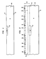
- FIG. 2 there is shown wafer 10 after further processing with a (grown p-type) first epitaxial layer 14 over the top surface 11 of the wafer 10 which serves as a substrate.
- first portion of the first epitaxial layer 14 tends to be p-type because of autodoping, (the outdiffusion of the p-type dopant in layer 12 into the epitaxial layer), it is feasible to begin the growth of this first epitaxial layer 14 without intentional doping but then to continue the growth in a p-type ambient in the usual fashion to insure that the growth will continue to be p-type.
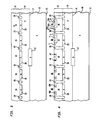
- n-type emitter zones 50a of the vertical transistors 50 This can be followed by a common step for the selective introduction of donor atoms to form the n-type emitter zones 50a of the vertical transistors 50, and to form (heavily doped) n-type surface regions 50c to define the collector contact regions in the vertical transistors 50 and the base contact regions (not shown) in the lateral transistor 48.
- N-type pockets 30 serve as the base regions of each of lateral transistors 48.
- the introductions of the donor and acceptor atoms are localized to selected regions in the usual fashion, for example, by appropriate masks on the surface that have been patterned by photolithographic techniques familiar in integrated circuit technology.
- FIG. 6 there is shown an exploded top view of pocket 32 and the surrounding p-type pocket 28 which are shown in cross-sectional view in Figures 4 and 5.
- the broken line 36 is the outline of the diaphragm (that is, the exposed portion of a lower surface of p-type layer 12 which is denoted as, typically a square, to be formed by thinning wafer 10, and the four piezoresistors 41, 42, 43 and 44 are seen to be positioned around the outline.
- Each is shown provided at each of its ends with a contact region for connection into a Wheatstone bridge.
Landscapes
- Chemical & Material Sciences (AREA)
- Analytical Chemistry (AREA)
- Physics & Mathematics (AREA)
- General Physics & Mathematics (AREA)
- Engineering & Computer Science (AREA)
- Manufacturing & Machinery (AREA)
- Microelectronics & Electronic Packaging (AREA)
- Pressure Sensors (AREA)
- Measuring Fluid Pressure (AREA)
Applications Claiming Priority (2)
| Application Number | Priority Date | Filing Date | Title |
|---|---|---|---|
| US07/189,446 US4885621A (en) | 1988-05-02 | 1988-05-02 | Monolithic pressure sensitive integrated circuit |
| US189446 | 1988-05-02 |
Publications (3)
| Publication Number | Publication Date |
|---|---|
| EP0340904A2 EP0340904A2 (en) | 1989-11-08 |
| EP0340904A3 EP0340904A3 (en) | 1991-02-27 |
| EP0340904B1 true EP0340904B1 (en) | 1992-12-02 |
Family
ID=22697370
Family Applications (1)
| Application Number | Title | Priority Date | Filing Date |
|---|---|---|---|
| EP89303134A Expired - Lifetime EP0340904B1 (en) | 1988-05-02 | 1989-03-30 | Monolithic pressure sensitive integrated circuit and a process for manufacture thereof |
Country Status (5)
| Country | Link |
|---|---|
| US (1) | US4885621A (ja) |
| EP (1) | EP0340904B1 (ja) |
| JP (1) | JPH01318265A (ja) |
| KR (1) | KR920007827B1 (ja) |
| DE (1) | DE68903674T2 (ja) |
Families Citing this family (16)
| Publication number | Priority date | Publication date | Assignee | Title |
|---|---|---|---|---|
| US5397911A (en) * | 1991-04-02 | 1995-03-14 | Honda Giken Kogyo Kabushiki Kaisha | Semiconductor sensor with plural gate electrodes |
| JP3009239B2 (ja) * | 1991-04-02 | 2000-02-14 | 本田技研工業株式会社 | 半導体センサ |
| JPH05190872A (ja) * | 1992-01-16 | 1993-07-30 | Oki Electric Ind Co Ltd | 半導体圧力センサおよびその製造方法 |
| US6140143A (en) * | 1992-02-10 | 2000-10-31 | Lucas Novasensor Inc. | Method of producing a buried boss diaphragm structure in silicon |
| DE4206174C2 (de) * | 1992-02-28 | 1995-06-22 | Bosch Gmbh Robert | Integrierter Sensor aus Silizium |
| US5427975A (en) * | 1993-05-10 | 1995-06-27 | Delco Electronics Corporation | Method of micromachining an integrated sensor on the surface of a silicon wafer |
| DE69512544T2 (de) * | 1994-03-18 | 2000-05-25 | The Foxboro Co., Foxboro | Halbleiter-Druckwandler mit Einkristall-Silizium-Membran und Einkristall-Dehnungsmessstreifen und Herstellungsverfahren dazu |
| JP3624597B2 (ja) * | 1996-12-10 | 2005-03-02 | 株式会社デンソー | 半導体装置及びその製造方法 |
| DE19741428A1 (de) * | 1997-09-19 | 1999-04-01 | Siemens Ag | Halbleitersensor mit einem Grundkörper und wenigstens einem Verformungskörper |
| US6278167B1 (en) | 1998-08-14 | 2001-08-21 | Infineon Technologies Ag | Semiconductor sensor with a base element and at least one deformation element |
| US6142021A (en) * | 1998-08-21 | 2000-11-07 | Motorola, Inc. | Selectable pressure sensor |
| US20020003274A1 (en) * | 1998-08-27 | 2002-01-10 | Janusz Bryzek | Piezoresistive sensor with epi-pocket isolation |
| US6229190B1 (en) | 1998-12-18 | 2001-05-08 | Maxim Integrated Products, Inc. | Compensated semiconductor pressure sensor |
| JP4710147B2 (ja) * | 2000-06-13 | 2011-06-29 | 株式会社デンソー | 半導体圧力センサ |
| DE10057656C1 (de) * | 2000-11-21 | 2002-04-04 | Rossendorf Forschzent | Verfahren zur Herstellung von integrierten Abtastnadeln |
| CN102664161B (zh) * | 2012-05-25 | 2016-11-16 | 杭州士兰集成电路有限公司 | 高压bcd工艺中高压器件的隔离结构及其制造方法 |
Family Cites Families (14)
| Publication number | Priority date | Publication date | Assignee | Title |
|---|---|---|---|---|
| US3994009A (en) * | 1973-02-12 | 1976-11-23 | Honeywell Inc. | Stress sensor diaphragms over recessed substrates |
| US3858150A (en) * | 1973-06-21 | 1974-12-31 | Motorola Inc | Polycrystalline silicon pressure sensor |
| US4003127A (en) * | 1974-11-25 | 1977-01-18 | General Motors Corporation | Polycrystalline silicon pressure transducer |
| CA1047652A (en) * | 1975-07-31 | 1979-01-30 | National Semiconductor Corporation | Monolithic integrated circuit transistor having very low collector resistance |
| US4033787A (en) * | 1975-10-06 | 1977-07-05 | Honeywell Inc. | Fabrication of semiconductor devices utilizing ion implantation |
| JPS5583227A (en) * | 1978-12-20 | 1980-06-23 | Matsushita Electronics Corp | Epitaxial growing |
| US4372803A (en) * | 1980-09-26 | 1983-02-08 | The United States Of America As Represented By The Secretary Of The Navy | Method for etch thinning silicon devices |
| US4332000A (en) * | 1980-10-03 | 1982-05-25 | International Business Machines Corporation | Capacitive pressure transducer |
| US4456901A (en) * | 1981-08-31 | 1984-06-26 | Kulite Semiconductor Products, Inc. | Dielectrically isolated transducer employing single crystal strain gages |
| JPS59117271A (ja) * | 1982-12-24 | 1984-07-06 | Hitachi Ltd | 圧力感知素子を有する半導体装置とその製造法 |
| JPS59136977A (ja) * | 1983-01-26 | 1984-08-06 | Hitachi Ltd | 圧力感知半導体装置とその製造法 |
| JPS60128673A (ja) * | 1983-12-16 | 1985-07-09 | Hitachi Ltd | 半導体感圧装置 |
| JPS6269547A (ja) * | 1985-09-24 | 1987-03-30 | Hitachi Ltd | 半導体装置 |
| JPS62266876A (ja) * | 1986-05-14 | 1987-11-19 | Nippon Denso Co Ltd | 半導体圧力センサ |
-
1988
- 1988-05-02 US US07/189,446 patent/US4885621A/en not_active Expired - Fee Related
-
1989
- 1989-03-30 EP EP89303134A patent/EP0340904B1/en not_active Expired - Lifetime
- 1989-03-30 DE DE8989303134T patent/DE68903674T2/de not_active Expired - Fee Related
- 1989-05-02 JP JP1113607A patent/JPH01318265A/ja active Pending
- 1989-05-02 KR KR1019890005918A patent/KR920007827B1/ko not_active Expired
Also Published As
| Publication number | Publication date |
|---|---|
| DE68903674D1 (de) | 1993-01-14 |
| KR920007827B1 (ko) | 1992-09-17 |
| JPH01318265A (ja) | 1989-12-22 |
| DE68903674T2 (de) | 1993-04-01 |
| EP0340904A2 (en) | 1989-11-08 |
| US4885621A (en) | 1989-12-05 |
| EP0340904A3 (en) | 1991-02-27 |
| KR900019278A (ko) | 1990-12-24 |
Similar Documents
| Publication | Publication Date | Title |
|---|---|---|
| EP0340904B1 (en) | Monolithic pressure sensitive integrated circuit and a process for manufacture thereof | |
| US5719069A (en) | One-chip integrated sensor process | |
| US4904978A (en) | Mechanical sensor for high temperature environments | |
| US5552347A (en) | Fabrication process for a semiconductor pressure sensor for sensing pressure applied thereto | |
| US4618397A (en) | Method of manufacturing semiconductor device having a pressure sensor | |
| US6122975A (en) | CMOS compatible integrated pressure sensor | |
| US4977101A (en) | Monolithic pressure sensitive integrated circuit | |
| US5178016A (en) | Silicon pressure sensor chip with a shear element on a sculptured diaphragm | |
| JP2940293B2 (ja) | 半導体加速度センサの製造方法 | |
| US7687298B2 (en) | Microelectromechanical device with integrated conductive shield | |
| US3893228A (en) | Silicon pressure sensor | |
| US4945769A (en) | Semiconductive structure useful as a pressure sensor | |
| US4721938A (en) | Process for forming a silicon pressure transducer | |
| US5589810A (en) | Semiconductor pressure sensor and related methodology with polysilicon diaphragm and single-crystal gage elements | |
| US4588472A (en) | Method of fabricating a semiconductor device | |
| US5672551A (en) | Method for manufacturing a semiconductor pressure sensor with single-crystal silicon diaphragm and single-crystal gage elements | |
| US5172205A (en) | Piezoresistive semiconductor device suitable for use in a pressure sensor | |
| US4706100A (en) | High temperature hetero-epitaxial pressure sensor | |
| JP3503146B2 (ja) | 半導体装置の製造方法 | |
| CN115985851A (zh) | 压力传感器的制作方法及压力传感器 | |
| GB2151398A (en) | A semiconductor pressure sensor and a method of manufacture thereof | |
| JP4845308B2 (ja) | 半導体センサ及びその製造方法 | |
| JPH05102494A (ja) | シリコンダイアフラム圧力センサの製造方法 | |
| JPS62266875A (ja) | 半導体圧力センサ | |
| EP0434318A2 (en) | Low sheet resistance diffused contacts to buried diffused resistors using isolation regions and buried layer |
Legal Events
| Date | Code | Title | Description |
|---|---|---|---|
| PUAI | Public reference made under article 153(3) epc to a published international application that has entered the european phase |
Free format text: ORIGINAL CODE: 0009012 |
|
| AK | Designated contracting states |
Kind code of ref document: A2 Designated state(s): DE FR GB |
|
| PUAL | Search report despatched |
Free format text: ORIGINAL CODE: 0009013 |
|
| AK | Designated contracting states |
Kind code of ref document: A3 Designated state(s): DE FR GB |
|
| 17P | Request for examination filed |
Effective date: 19910422 |
|
| 17Q | First examination report despatched |
Effective date: 19920406 |
|
| GRAA | (expected) grant |
Free format text: ORIGINAL CODE: 0009210 |
|
| AK | Designated contracting states |
Kind code of ref document: B1 Designated state(s): DE FR GB |
|
| REF | Corresponds to: |
Ref document number: 68903674 Country of ref document: DE Date of ref document: 19930114 |
|
| ET | Fr: translation filed | ||
| PLBE | No opposition filed within time limit |
Free format text: ORIGINAL CODE: 0009261 |
|
| STAA | Information on the status of an ep patent application or granted ep patent |
Free format text: STATUS: NO OPPOSITION FILED WITHIN TIME LIMIT |
|
| 26N | No opposition filed | ||
| PGFP | Annual fee paid to national office [announced via postgrant information from national office to epo] |
Ref country code: FR Payment date: 19960329 Year of fee payment: 8 |
|
| PGFP | Annual fee paid to national office [announced via postgrant information from national office to epo] |
Ref country code: DE Payment date: 19960509 Year of fee payment: 8 |
|
| PGFP | Annual fee paid to national office [announced via postgrant information from national office to epo] |
Ref country code: GB Payment date: 19970217 Year of fee payment: 9 |
|
| PG25 | Lapsed in a contracting state [announced via postgrant information from national office to epo] |
Ref country code: FR Free format text: LAPSE BECAUSE OF NON-PAYMENT OF DUE FEES Effective date: 19971128 |
|
| PG25 | Lapsed in a contracting state [announced via postgrant information from national office to epo] |
Ref country code: DE Effective date: 19971202 |
|
| REG | Reference to a national code |
Ref country code: FR Ref legal event code: ST |
|
| PG25 | Lapsed in a contracting state [announced via postgrant information from national office to epo] |
Ref country code: GB Free format text: LAPSE BECAUSE OF NON-PAYMENT OF DUE FEES Effective date: 19980330 |
|
| GBPC | Gb: european patent ceased through non-payment of renewal fee |
Effective date: 19980330 |