EP0342096A1 - Logischer Signalgenerator und Signal-Sequenzschaltung für Ladungsübertragungsvorrichtung - Google Patents
Logischer Signalgenerator und Signal-Sequenzschaltung für Ladungsübertragungsvorrichtung Download PDFInfo
- Publication number
- EP0342096A1 EP0342096A1 EP89401223A EP89401223A EP0342096A1 EP 0342096 A1 EP0342096 A1 EP 0342096A1 EP 89401223 A EP89401223 A EP 89401223A EP 89401223 A EP89401223 A EP 89401223A EP 0342096 A1 EP0342096 A1 EP 0342096A1
- Authority
- EP
- European Patent Office
- Prior art keywords
- signals
- transfer device
- charge transfer
- global bus
- sequencing
- Prior art date
- Legal status (The legal status is an assumption and is not a legal conclusion. Google has not performed a legal analysis and makes no representation as to the accuracy of the status listed.)
- Ceased
Links
Images
Classifications
-
- H—ELECTRICITY
- H03—ELECTRONIC CIRCUITRY
- H03K—PULSE TECHNIQUE
- H03K5/00—Manipulating of pulses not covered by one of the other main groups of this subclass
- H03K5/15—Arrangements in which pulses are delivered at different times at several outputs, i.e. pulse distributors
- H03K5/15013—Arrangements in which pulses are delivered at different times at several outputs, i.e. pulse distributors with more than two outputs
- H03K5/1506—Arrangements in which pulses are delivered at different times at several outputs, i.e. pulse distributors with more than two outputs with parallel driven output stages; with synchronously driven series connected output stages
- H03K5/15066—Arrangements in which pulses are delivered at different times at several outputs, i.e. pulse distributors with more than two outputs with parallel driven output stages; with synchronously driven series connected output stages using bistable devices
-
- G—PHYSICS
- G11—INFORMATION STORAGE
- G11C—STATIC STORES
- G11C27/00—Electric analogue stores, e.g. for storing instantaneous values
- G11C27/04—Shift registers
-
- H—ELECTRICITY
- H03—ELECTRONIC CIRCUITRY
- H03K—PULSE TECHNIQUE
- H03K5/00—Manipulating of pulses not covered by one of the other main groups of this subclass
- H03K5/15—Arrangements in which pulses are delivered at different times at several outputs, i.e. pulse distributors
- H03K5/15013—Arrangements in which pulses are delivered at different times at several outputs, i.e. pulse distributors with more than two outputs
- H03K5/1502—Arrangements in which pulses are delivered at different times at several outputs, i.e. pulse distributors with more than two outputs programmable
Definitions
- the present invention relates to a generator and sequencer circuit of logic signals for charge transfer devices.
- the charge transfer devices need, for their control, to receive a relatively large number of logic control signals, having a very precise temporal sequencing as well as regards the respective times when the pulses forming these logic signals are produced as the respective phases of these.
- logic control signals are used in particular to transfer the charges inside the matrix sensor (horizontal transfer, vertical transfer, transfer from the image plane to the memory plane, etc.), the delivery of the output signal with precise timing. and as a function of an external synchronization signal, the resets to zero, etc. It is these signals which will be designated subsequently by the general term of "logic control signals”.
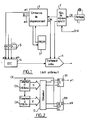
- a clock 1 generally quartz, produces a reference clock signal CK, of the order of 8 to 15 MHz, applied to a synchronized signal generator 2 which also receives an external SYN synchronization pulse intended for the synchronization of successive frames, this SYN signal generally being a signal at 50 or 60 Hz.
- the output signal from the synchronized signal generator 2 is applied as input to a sequencing control circuit 3 which produces the various logic control signals ⁇ 1 ... ⁇ N necessary for controlling the charge transfer device 4, via a "driver" stage 5 which adapts the voltage and current levels according to the needs of the charge transfer device.
- the sequencing command generally produces signals of the TTL type, that is to say of which the two logic levels correspond to 0 and 5 volts, voltages which are not those which the sensor needs to operate; in addition, the current drawn by the sensor is generally much greater than the possibilities of the sequencing logic circuit, usually a circuit in MOS technology.
- the charge transfer devices generally comprising a certain number of defective pixels, these faults are corrected so as to make them invisible (for example by reproducing, for the defective pixel, the voltage level corresponding to the illumination of the pixel immediately preceding).
- This correction is carried out, on command of the sequencing circuit 3, by the circuit 6 ensuring the processing of the video signal delivered at the output of the sensor 4.
- the positions of the defective pixels have been previously stored in an external memory 7, generally a PROM delivered at the same time as the sensor whose faults it memorizes.
- the sequencing control circuit 3 is connected to the PROM 7 by an address bus and a data bus and, on each line, it interrogates the PROM to find out if there is a defect on this line and, if so, what is the horizontal position of this defective pixel. It will then deliver the COR signal to the video processing circuit 6 at the appropriate time (it should be noted in this regard that it is thus only possible to memorize one defective pixel per line, which is generally sufficient but requires elimination by sorting sensors that do not meet this condition).
- the sequencing control circuit is a circuit specific to a particular sensor (for example, for a sensor of the Sony ICX021L type, the corresponding sequencing control circuit will be CX23047A, associated with a CX7930 synchronized signal generator and a PROM MB6052).
- circuits 2, 3 and 7 are, on the scale of the sensor, relatively bulky insofar as it is necessary to provide several different discrete circuits (circuits 2, 3 and 7) with their respective interconnections.
- circuits 2, 3 and 7 into a single integrated component since memory 7 contains specific programming associated with a given copy of sensor, and it is always necessary for the PROM to remain separate from the rest of the circuit so that it can be exchanged if, for example, the sensor is exchanged.
- the present invention proposes to overcome these drawbacks by proposing a generator and sequencer circuit of logic signals for charge transfer devices which, not only, integrates in a single box the various functions necessary for controlling the charge transfer device, but also is of universal design, that is to say that, unlike dedicated circuits of the prior art, the circuit of the present invention is compatible with almost all existing sensors.
- This particularly advantageous characteristic makes it possible to have only a single video sequencing / processing card whatever the sensor used, only the stage for adapting the voltages and currents ("driver" circuit 5 in FIG. 1) being specific. to the sensors.
- circuit of the invention allows to find one of the advantages which was previously available in tube cameras, namely that one could change the type of tubes without having changing the associated frame and line synchronization circuits.
- the circuit generating and sequencing logic signals for charge transfer device having an input intended to receive a reference clock signal (CK), and comprising means for generating synchronized logic signals connected to means for sequencing these logic signals so as to output the plurality of logic clock control signals ( ⁇ 1 ... ⁇ N) necessary for controlling the charge transfer device, is characterized in that the generation and sequencing means are integrated into a single component of the programmable logic component type - preferably erasable and reprogrammable -, the programming of the component being carried out according to the characteristics of the charge transfer device used.
- CK reference clock signal
- the programmable logic component is configured so as to include, around a common global bus: first synchronized signal generating means, receiving said clock signal as input and applying as output to the global bus a succession of first binary configurations representative of the horizontal sequencing of the charge transfer device, - second synchronized signal generating means, receiving as input a signal corresponding to the appearance of a particular binary configuration among said first binary configurations, and applying as output on the global bus a succession of second binary configurations representative of the vertical sequencing of the charge transfer device, and a plurality of sequencing means arranged in parallel on the global bus, these sequencing means receiving as input the signals present on the global bus and decoding these signals so as to generate respectively, at a given instant as a function of said binary configurations and said signal clock, one of said logic control signals.
- the generator and sequencer circuit further comprises fault detecting means receiving as input the signals present on the global bus and decoding these signals so as to generate, for certain predefined combinations corresponding to positions of defective pixels of the transfer device charge, a fault correction signal delivered to the circuit ensuring the processing of the video signal produced at the output of the charge transfer device.
- the generator and sequencer circuit is essentially formed by a circuit of the programmable logic component type, very advantageously of the reprogrammable type, component better known by its name PLD (Programmable Logic Device) or EPLD (Erasable Programmable Logic Device).
- PLD Programmable Logic Device
- EPLD Erasable Programmable Logic Device
- circuits include a certain number of prediffused logic functions or "macrocells” comprising the conventional logic functions such as flip-flops, doors, etc. ; these macrocells are then configured together by the user by means of EPROM transistors programmed so as to make the desired logical connections (the term “programmable” will be understood in the usual sense of “writable” that is given to it in EPROM technology or EEPROM; this term must not evoke microprogrammed logic, but only wired logic configured in a certain way by selective recording of certain data defining the logic configuration that the circuit must present).
- programmable will be understood in the usual sense of "writable” that is given to it in EPROM technology or EEPROM; this term must not evoke microprogrammed logic, but only wired logic configured in a certain way by selective recording of certain data defining the logic configuration that the circuit must present).
- An internal "global bus”, to which all the macrocells can be connected, allows them to communicate with each other and with component input / output ports.
- Such a circuit suitable for implementing the invention is for example the EP1800 from Altera, which is a circuit with 48 macrocells, each including a flip-flop and a set of elementary logic functions, for a total of 2100 equivalent gates.
- This component is however only given by way of illustration and, in general, one could as well use any type of programmable logic component comprising at least 1500 equivalent logic gates and at least 40 RS flip-flops; if it is desired to incorporate the fault detection function into the circuit of the invention, the programmable logic component must be of the reprogrammable type.
- the essential principle is that illustrated in FIG. 2: the clock pulses CK produced by the external clock are applied to a first counter CH intended to ensure the horizontal sequencing of the frame scanning of the sensor.
- This register is for example a ten-stage register, which therefore outputs a first binary configuration (symbolized by the H bus) which can take 1024 different states.
- This first counter CH drives a second counter CV intended to ensure the vertical sequencing of the frame scanning of the sensor.
- This second CV counter is for example an eleven-stage counter, which therefore outputs a second binary configuration (symbolized by the V bus) which can take 2048 different states.
- the two logic configurations H and V are decoded by a stage D which makes it possible to control the positioning and the depositioning of a series of flip-flops B1 ... BN whose outputs will constitute the logic signals ⁇ 1 ... ⁇ N for controlling the device load transfer (the exact number of outputs ⁇ 1 ... ⁇ N actually depends on the type of component used).
- These logic control signals ⁇ 1 ... ⁇ N typically include the vertical and horizontal transfer clocks (requiring two or four signals, depending on the components) and the reset clock signals of the output stage; other logic signals can possibly be provided according to the different particular cases.
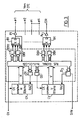
- FIG. 3 shows more precisely the manner in which the circuit of FIG. 2 is arranged inside a circuit of the programmable logic component type.
- the horizontal synchronization counter CH is reset to zero by a pulse delivered at each end of line by a decoder stage D1.
- the decoder stage D1 being programmed as a function of the number of pixels per line, it can be seen that, if the sensor is changed to a sensor comprising a higher number of pixels per line, it suffices to modify the programming of this decoder stage D1, without further change.
- the vertical synchronization counter CV is attacked at its clock input by the output of a similar decoder D2 in response to each start of a new line, and it is reset to zero by a decoder D3 in response to each end of frame (function of the number of lines per frame) and also of the external synchronization signal SYN.
- the different flip-flops B1 ... BN are controlled at each of their R and S inputs by a detector stage DB1, DB1 ′, ... analyzing the signals present on the global bus and receiving on its input CK the clock pulses, which also pass through the global bus.
- the outputs Q of the flip-flops are applied, via an adapter stage P1, ... to the various clock inputs ⁇ 1 ... ⁇ N of the charge transfer device.
- the outputs Q of the flip-flops are also applied to specific lines of the bus so as to ensure perfect synchronization of the different signals, exactly respecting their respective phase.
- an additional stage comprising a flip-flop BX and associated decoders DBX, DBX ′ which deliver to the video processing circuit (circuit 6 in FIG. 1), via stage PX, a signal COR for correcting defaults.
- the DBX and DBX ′ detectors are programmed specifically for each sensor copy, according to the positions of the defective pixels previously identified (unlike the decoders D1, D2, D3 and DB1, DB1 ′, ... DBN, DBN ′, which only depend on the type of sensor and are therefore programmed in the same way for all the copies of the same type of sensor).
- the programmable logic component is reprogrammable, it will suffice to reprogram it in the event of the replacement of a defective sensor, without modification or exchange of any component.
Landscapes
- Physics & Mathematics (AREA)
- Nonlinear Science (AREA)
- Transforming Light Signals Into Electric Signals (AREA)
- Manipulation Of Pulses (AREA)
Applications Claiming Priority (2)
| Application Number | Priority Date | Filing Date | Title |
|---|---|---|---|
| FR8806281A FR2631502A1 (fr) | 1988-05-10 | 1988-05-10 | Circuit generateur et sequenceur de signaux logiques pour dispositif a transfert de charges |
| FR8806281 | 1988-05-10 |
Publications (1)
| Publication Number | Publication Date |
|---|---|
| EP0342096A1 true EP0342096A1 (de) | 1989-11-15 |
Family
ID=9366170
Family Applications (1)
| Application Number | Title | Priority Date | Filing Date |
|---|---|---|---|
| EP89401223A Ceased EP0342096A1 (de) | 1988-05-10 | 1989-04-28 | Logischer Signalgenerator und Signal-Sequenzschaltung für Ladungsübertragungsvorrichtung |
Country Status (4)
| Country | Link |
|---|---|
| US (1) | US4980770A (de) |
| EP (1) | EP0342096A1 (de) |
| JP (1) | JPH01319374A (de) |
| FR (1) | FR2631502A1 (de) |
Families Citing this family (2)
| Publication number | Priority date | Publication date | Assignee | Title |
|---|---|---|---|---|
| US5162913A (en) * | 1990-02-26 | 1992-11-10 | Medical Concepts, Inc. | Apparatus for modulating the output of a ccd camera |
| JP2001238138A (ja) * | 2000-02-21 | 2001-08-31 | Matsushita Electric Ind Co Ltd | 固体撮像素子のためのタイミングジェネレータ |
Citations (2)
| Publication number | Priority date | Publication date | Assignee | Title |
|---|---|---|---|---|
| US4291241A (en) * | 1978-02-20 | 1981-09-22 | Hitachi, Ltd. | Timing signal generating circuit |
| US4431926A (en) * | 1978-05-24 | 1984-02-14 | Nippon Electric Co., Ltd. | Counter controlled signal generator |
Family Cites Families (4)
| Publication number | Priority date | Publication date | Assignee | Title |
|---|---|---|---|---|
| JPS6034872B2 (ja) * | 1977-01-28 | 1985-08-10 | ソニー株式会社 | 固体撮像装置の雑音除去回路 |
| US4280141A (en) * | 1978-09-22 | 1981-07-21 | Mccann David H | Time delay and integration detectors using charge transfer devices |
| US4399464A (en) * | 1981-05-04 | 1983-08-16 | General Dynamics, Pomona Division | Signal processor for an array of CID radiation detector elements |
| FR2566219B1 (fr) * | 1984-06-15 | 1989-04-28 | Sfim | Procede et dispositif pour l'exploration d'une fenetre de la zone image d'un dispositif a transfert de charges du type a transfert de trames |
-
1988
- 1988-05-10 FR FR8806281A patent/FR2631502A1/fr active Pending
-
1989
- 1989-04-28 EP EP89401223A patent/EP0342096A1/de not_active Ceased
- 1989-05-10 JP JP1115226A patent/JPH01319374A/ja active Pending
- 1989-05-10 US US07/349,831 patent/US4980770A/en not_active Expired - Fee Related
Patent Citations (2)
| Publication number | Priority date | Publication date | Assignee | Title |
|---|---|---|---|---|
| US4291241A (en) * | 1978-02-20 | 1981-09-22 | Hitachi, Ltd. | Timing signal generating circuit |
| US4431926A (en) * | 1978-05-24 | 1984-02-14 | Nippon Electric Co., Ltd. | Counter controlled signal generator |
Non-Patent Citations (4)
| Title |
|---|
| ELECTRONIC DESIGN, vol. 29, no. 16, 6 août 1981, pages 183-190, Waseca, MN., US; A.P. KING et al.: "Charge-coupled devices tackle TV imaging" * |
| ELECTRONICS INTERNATIONAL, vol. 50, no. 8, 14 avril 1977, pages 107-108, New York, US; C. BOLON: "Decoders drive flip-flops for clean multiphase clock" * |
| IBM TECHNICAL DISCLOSURE BULLETIN, vol. 22, no. 6, novembre 1979, pages 2301-2302, New York, US; F.J. AICHELMANN, Jr.: "Bypass selection machanism for defective chips" * |
| PATENT ABSTRACTS OF JAPAN, vol. 13, no. 34 (E-708)[3382], 25th January 1989; & JP-A-63 233 607 (FUJITSU LTD) 29-09-1988 * |
Also Published As
| Publication number | Publication date |
|---|---|
| US4980770A (en) | 1990-12-25 |
| FR2631502A1 (fr) | 1989-11-17 |
| JPH01319374A (ja) | 1989-12-25 |
Similar Documents
| Publication | Publication Date | Title |
|---|---|---|
| EP0178954B1 (de) | Verfahren und Einrichtung zur Abtastung eines Fensters im Bildbereich einer bildorganisierten Ladungsübertragungsanordnung | |
| EP0265326A1 (de) | Verfahren zur Steuerung einer elektrooptischen Matrixanzeige und dafür geeignete Steuerungsschaltung | |
| FR2476851A1 (fr) | Procedes et appareils de controle automatique de circuits electriques | |
| FR2682785A1 (fr) | Structure de microprocesseur a frequence de noyau double de celle des bus. | |
| WO1991012690A1 (fr) | Dispositif d'augmentation de dynamique d'une camera | |
| EP0142439A2 (de) | Verfahren zur Kompression einer Folge digitaler Informationen und Vorrichtung dafür | |
| EP0441692A1 (de) | Verfahren zur Steuerung eines Matrixbildschirms, bestehend aus zwei unabhängigen Teilen und Einrichtung zu seiner Durchführung | |
| EP0517335A1 (de) | Frequenzteilerschaltung | |
| EP3423978B1 (de) | Verfahren eine animation zum anzeigen wahrend dem start eines geräts | |
| EP0474541B1 (de) | Verfahren und Vorrichtung zur Taktsignalregelung in einem Synchronsystem | |
| EP0222641A1 (de) | Einrichtungen für elektronische Überblendung | |
| FR2631502A1 (fr) | Circuit generateur et sequenceur de signaux logiques pour dispositif a transfert de charges | |
| FR2532777A1 (fr) | Circuit de translation de signaux | |
| EP2130097B1 (de) | Verfahren zum zugreifen einen nichtflüchtigen speicher für eine uhr | |
| EP0206844B1 (de) | Festwertspeicher mit einmaliger elektrischer Einschreibemöglichkeit | |
| EP0513325A1 (de) | Pulsbreitenmodulationsgenerator mit zeitvernier | |
| EP0833346A1 (de) | Serieller Zugriffspeicher mit sicherem Schreiben | |
| FR2498858A1 (fr) | Dispositif de convergence pour camera couleurs | |
| EP0267091A1 (de) | Elektrisch programmierbarer Festwertspeicher | |
| FR2604554A1 (fr) | Dispositif de securite pourla programmation d'une memoire non volatile programmable electriquement | |
| EP0526359A1 (de) | Verfahren und Schaltungsanordnung zur Synchronisierung eines Signals | |
| FR2788353A1 (fr) | Microprocesseur avec circuits de protection pour securiser l'acces a ses registres | |
| CN108195371A (zh) | 基于dmd的高动态多星体目标的提取方法、装置及系统 | |
| FR2575888A1 (fr) | Procede et dispositif de mise au point d'une camera et camera comportant un tel dispositif | |
| EP0640910B1 (de) | Verfahren zur Steuerung einer FIFO-Schaltung und Einrichtung zu seiner Durchführung |
Legal Events
| Date | Code | Title | Description |
|---|---|---|---|
| PUAI | Public reference made under article 153(3) epc to a published international application that has entered the european phase |
Free format text: ORIGINAL CODE: 0009012 |
|
| AK | Designated contracting states |
Kind code of ref document: A1 Designated state(s): DE ES GB IT |
|
| 17P | Request for examination filed |
Effective date: 19891202 |
|
| 17Q | First examination report despatched |
Effective date: 19910920 |
|
| STAA | Information on the status of an ep patent application or granted ep patent |
Free format text: STATUS: THE APPLICATION HAS BEEN REFUSED |
|
| 18R | Application refused |
Effective date: 19920920 |