EP0142439A2 - Verfahren zur Kompression einer Folge digitaler Informationen und Vorrichtung dafür - Google Patents
Verfahren zur Kompression einer Folge digitaler Informationen und Vorrichtung dafür Download PDFInfo
- Publication number
- EP0142439A2 EP0142439A2 EP84402265A EP84402265A EP0142439A2 EP 0142439 A2 EP0142439 A2 EP 0142439A2 EP 84402265 A EP84402265 A EP 84402265A EP 84402265 A EP84402265 A EP 84402265A EP 0142439 A2 EP0142439 A2 EP 0142439A2
- Authority
- EP
- European Patent Office
- Prior art keywords
- difference
- word
- absolute value
- value
- memory
- Prior art date
- Legal status (The legal status is an assumption and is not a legal conclusion. Google has not performed a legal analysis and makes no representation as to the accuracy of the status listed.)
- Granted
Links
- 238000000034 method Methods 0.000 title claims description 17
- 230000015654 memory Effects 0.000 claims abstract description 65
- 230000006835 compression Effects 0.000 claims abstract description 17
- 238000007906 compression Methods 0.000 claims abstract description 17
- 238000012546 transfer Methods 0.000 claims abstract description 14
- 230000006870 function Effects 0.000 claims 1
- 238000012360 testing method Methods 0.000 description 8
- 238000012545 processing Methods 0.000 description 7
- 238000010586 diagram Methods 0.000 description 4
- 230000008901 benefit Effects 0.000 description 2
- 230000008859 change Effects 0.000 description 2
- 238000006243 chemical reaction Methods 0.000 description 2
- 230000000295 complement effect Effects 0.000 description 2
- 239000004065 semiconductor Substances 0.000 description 2
- 230000005540 biological transmission Effects 0.000 description 1
- 239000008280 blood Substances 0.000 description 1
- 210000004369 blood Anatomy 0.000 description 1
- 239000002872 contrast media Substances 0.000 description 1
- 238000011161 development Methods 0.000 description 1
- 230000000694 effects Effects 0.000 description 1
- 235000021183 entrée Nutrition 0.000 description 1
- 230000008569 process Effects 0.000 description 1
- 230000033764 rhythmic process Effects 0.000 description 1
- 230000002123 temporal effect Effects 0.000 description 1
- 238000013518 transcription Methods 0.000 description 1
- 230000035897 transcription Effects 0.000 description 1
- 230000007704 transition Effects 0.000 description 1
- 238000010200 validation analysis Methods 0.000 description 1
Images


Classifications
-
- H—ELECTRICITY
- H04—ELECTRIC COMMUNICATION TECHNIQUE
- H04N—PICTORIAL COMMUNICATION, e.g. TELEVISION
- H04N19/00—Methods or arrangements for coding, decoding, compressing or decompressing digital video signals
- H04N19/50—Methods or arrangements for coding, decoding, compressing or decompressing digital video signals using predictive coding
- H04N19/593—Methods or arrangements for coding, decoding, compressing or decompressing digital video signals using predictive coding involving spatial prediction techniques
-
- H—ELECTRICITY
- H03—ELECTRONIC CIRCUITRY
- H03M—CODING; DECODING; CODE CONVERSION IN GENERAL
- H03M7/00—Conversion of a code where information is represented by a given sequence or number of digits to a code where the same, similar or subset of information is represented by a different sequence or number of digits
- H03M7/30—Compression; Expansion; Suppression of unnecessary data, e.g. redundancy reduction
-
- H—ELECTRICITY
- H03—ELECTRONIC CIRCUITRY
- H03M—CODING; DECODING; CODE CONVERSION IN GENERAL
- H03M7/00—Conversion of a code where information is represented by a given sequence or number of digits to a code where the same, similar or subset of information is represented by a different sequence or number of digits
- H03M7/30—Compression; Expansion; Suppression of unnecessary data, e.g. redundancy reduction
- H03M7/40—Conversion to or from variable length codes, e.g. Shannon-Fano code, Huffman code, Morse code
- H03M7/42—Conversion to or from variable length codes, e.g. Shannon-Fano code, Huffman code, Morse code using table look-up for the coding or decoding process, e.g. using read-only memory
Definitions
- the invention relates to a method of compressing a succession of binary digital information, in particular representative of the pixels of a digitized image; the invention also relates to a device implementing such a method.
- the values of the various elementary areas of the image or pixels are transcribed into words.
- the value of each word represents the "luminance" of the pixel considered.
- the radiological image is displayed by a luminance amplifier, captured by a camera and the signal from this camera is sampled.
- the series of samples thus produced represents for example a line by line reading by "scanning" of the different pixels of these lines. This series of samples is digitized, that is to say transformed into a series of words.
- each word is coded on 8 bits, which represents a gradation from 0 to 255 from black to white and if we define an image of 512 X 512 pixels
- the memory capacity is significant, that is 2,097,152 bits at to memorize.
- a mass memory is essential. We often use magnetic disk storage.
- a buffer memory of limited capacity is coupled to the mass memory, for the transfer of information. The mass memory is therefore "supplied" by successive readings of the information contained in the buffer memory.
- transferring the contents of the buffer memory to the mass memory is an operation which requires time and which limits the performance of the system to an insufficient rate of images in certain cases, for example if one wishes to observe phenomenons as rapid as the development of a contrast medium in the blood system or the heart. It is therefore advantageous to compress the information representative of an image by exploiting the spatial and / or temporal redundancies inherent in it.
- the compression ratio defines the gain achieved after treatment.
- a compression ratio of 2 means that a buffer memory having the capacity necessary to memorize a complete normal image, can also receive the information representative of two images, after compression.
- the rate of image acquisition can be doubled.
- variable length codes have already been proposed, for example the Huffman codes.
- Huffman codes Such a code results in a conversion table where each possible difference value (between - 255 and + 255 for the example mentioned above) receives a binary code of length inversely proportional to its frequency of appearance.
- the invention relates to several improvements to this type of coding.
- Another important characteristic of the invention consists in directly coding the value of the pixel as soon as the difference exceeds, in absolute value, a chosen number. Indeed, if we consider pixels coded on 8 bits, for example, a large difference value requires 9 bits to be coded, because of the sign of this difference. It then becomes advantageous to code the pixel directly on 8 bits, since it is necessarily a positive number. In the example which will be described later, the pixel is directly coded (on 8 bits) as soon as the difference exceeds 31 in absolute value.
- Another notable feature of the invention consists in defining given intervals of possible differences and in identifying each interval by a given prefix.
- This mode of identifying difference values has the advantage of reducing the "tree structure" of the electronic decoding circuits, that is to say the number of logic tests to be carried out before fully recognizing a word. So, for example, the recognition of the prefix can be used to address a table (read-only memory) directly containing all the possible values of differences in the interval corresponding to the prefix.
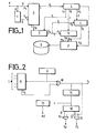
- FIG. 1 represents the block diagram of a circuit for compressing a succession of words representing the pixels of an image.
- the 8-bit words are in parallel form and are applied to an input E to undergo compression while the digital information resulting from this compression are recorded in series in a buffer memory 7.
- the latter is coupled to a mass memory 8 (magnetic disk system for example) and repeated readings of the buffer memory make it possible to "feed" the mass memory 8.
- the purpose of the compression is to increase the rate of acquisition of the images in spite of a rhythm of transfer relatively slow between memories 7 and 8.
- the compression method essentially consists in memorizing, not the 8-bit words representing the pixels but the difference between two successive pixels, using a variable length code.
- the input E is therefore connected to an input Xn of a processing circuit 2 which will be described later and to a register 1 forming a memory, the output of which is connected to an input Xn-1 of the processing circuit 2.
- the latter receives therefore at any time on its two inputs the value of a pixel and that of the previous pixel.
- the inputs E, Xn, X n-1 are 8-bit parallel inputs (that is to say each having 8 access terminals) and the register 1 is with parallel input and parallel output, also on 8 bits.
- each parallel link is conventionally represented by a single wire cut by an oblique line with which the number of bits of said link appears.
- Circuit 2 includes a parallel output C (of 16 bits) delivering the information (the code) to be recorded, coded and "formatted", as well as a parallel output L (of 4 bits) delivering information representative of the length of the code appearing simultaneously at the output C.
- the output L is applied to an input of a sequencer 4 comprising 3 clock outputs SI, S2 and S3 connected respectively to drive three registers of 8 bits, 3.5 and 6. L ' arrangement of the sequencer 4 will be described later.
- the output C of the processing circuit 2 is connected to the input of register 3 which is of the type with parallel loading and serial output.
- the sequencer decodes the useful length of the 16-bit "formatted" C code, to be transferred in series to register 5 or register 6. More precisely, the output SI delivers each time a number of pulses equal to the length L and this clock signal applied to register 3 controls the transfer of the most significant bits to register 5 or 6 which is validated by the corresponding clock S2 or S3.
- the output L programs the sequencer so that it generates only 4 clock pulses at the output SI so that only the word 1100 is written in one of the registers 5 or 6.
- the adopted format of 16 bits , for code C corresponds to the maximum length of the words to be transferred to memory 7.
- the serial output S4 of register 3 is connected to the inputs E 1 and E 2 of registers 5 and 6, respectively. These registers are of the serial input - parallel output type.
- the two outputs Se, S 6 of these registers are connected to a parallel input E 3 of the memory 7 which further comprises an addressing input Ad controlled by the sequencer 4.
- the presence of the two registers 5 and 6 is justified by the fact that the memory 7 is conventionally arranged in 8-bit addressable words.
- the clocks available at outputs S2 and S3 alternately validate registers 5 and 6.
- the sequencer switches following the unloading of register 3 to the other register 6 (or 5). At the same time it generates the address of the memory 7 to which the register 5 (or 6) must be unloaded.
- the sequencer is shown in FIG. 2. It includes a clock generator H which controls a down-counter 9 with parallel setpoint input, connected to the output L of circuit 2 and receiving therefore a word representative of the length of the code.
- the clock generator H is also connected to an input of an AND gate, 10 to two inputs, the output of which constitutes the output SI driving the register 3.
- the down-counter 9 includes an output S 9 called "zero state” which changes of state when the clock H has reset the down counter to zero, that is to say when it has delivered a number of pulses corresponding to the length L displayed at the setpoint input.
- This output S 9 is connected to the other input of the door 10. Its change of state blocks the door 10 and therefore interrupts the transmission of the clock pulses at the output S 1 .
- the output of the AND gate, 10 is also connected to the input of a counter 11. It is a counter by eight which controls a flip-flop 12 and an address counter 13. The output of the latter constitutes the output Ad which controls the memory 7.
- the output Q of the flip-flop 12 is connected to an input of an AND gate, 14, with two inputs while its output Q is connected to an input of an AND gate, 15 , with two entrances.
- the other two inputs of doors 14 and 15 are connected to the output S 1 .
- the outputs of doors 14 and 15 constitute the outputs S 2 and S 3 mentioned above.
- D n be the difference between two consecutive pixels: since X and X n-1 are whole numbers included in a given positive interval [0 to 255], D n is included in the interval [-255 + 255].
- the conversion of possible D values into binary code can be in accordance with the following table:
- D n 0, that is to say the most frequent statistically difference value in the succession of the pixels of the image, is coded with the word of minimum length, that is to say on a bit.
- the words of code sent arranged with an identification prefix and a suffix as well as (possibly) the sign bit S.
- the identification prefix designates a given range of absolute difference values. For example, for the double interval of differences [ ⁇ 8 to + 15] we define a first prefix 111110, for the double interval of differences [ ⁇ 16 to + 31], we define a second prefix 1111110, and for the double interval of differences [ ⁇ 32 to ⁇ 255] a third prefix 1111111 is defined.
- the suffix XYZ has a sufficient number of bits (three) to represent all the absolute values of possible differences in the interval [ ⁇ 8 to + 15], since 3 bits allow 8 binary combinations. It is the same for the interval [ ⁇ 16 to + 31], whose suffix comprises 4 bits: XYZT.
- the suffix ABCDEFGH represents the very value of the pixel. Indeed, beyond 31, the coding of the difference would require more bits, taking into account the need to code the sign S, than the coding of the pixel itself (always positive).
- this suffix with a third identification prefix, namely 1111111.
- the sign bit S is deleted during coding whenever possible.
- the conditions for suppressing the sign bit S can apply in theory over the entire range of the values of possible differences (i.e. [-255 to +255] in the described case) but that, due to the particularity of direct coding of the pixel in the double interval [ ⁇ 32 to + 255], these conditions have meaning only for the interval complementary [-31 to + 31] excluding zero.
- the examples which follow make it possible to understand the conditions for suppressing the bit of sign S.
- the inputs X n and X n- are directly connected to the inputs of a digital subtractor 20 including the parallel output D n (on 9 bits ) delivers the value of the difference at all times:
- TTL 181 the binary representation used in the subtractor is a two's complement representation
- a read only memory 21 PROM
- the read only memory 21 is addressed directly by the output D, that is to say that is to say that the parallel output D of the subtractor 20 is connected to an address input of the read-only memory, each value of D n constituting an address of the memory 21 where the corresponding absolute value is found.
- the capacity of the memory 21 is reduced since it must contain 512 words of 8 bits.
- the output S 5 and the input X n-1 are also connected to the two inputs (of the parallel type, 8 blts) of a digital adder 22 and to the two inputs of a digital subtractor 23, so as to carry out the two operations following
- the circuits 22 and 23 can be produced from the same type of integrated circuit as the subtractor 20.
- the "carry-over" output S 8 of the adder 22 and the “carry-over” output S 9 of the subtractor 23 are respectively connected to the two inputs of a door 25 of the Exclusive OR type.
- the output S 8 displays the value of the transfer bit of the operation X n-1 +
- the set (22,23,25) which has just been described carries out in a simple manner the set of tests (defined above) making it possible to determine whether the sign bit can be deleted or not.
- the output S 5 is connected to a comparator 26 which makes it possible to determine whether the absolute value of the difference D is greater than or less than 31.
- this comparator can be a simple OR gate with three inputs to which the three are connected last terminals of output S 5 (on which the most significant bits appear). As the number 31 is expressed by: 00011111 in binary, a higher number will necessarily have at least one of its three bits with high weights equal to 1.
- the output of this door is connected to a control input e 5 of a multiplexer 27, the outputs L and C of which are the outputs shown in FIG. 2.
- This multiplexer has two groups of inputs L 1 , Ci and L 2 , C 2 , respectively, and its role is simply to match the inputs L 1 , Ci or L 2 , C 2 with the outputs L, C according to the command applied to the input e 5 .
- the input L 1 is fixed and expresses the number 15 in binary, the 8 terminals corresponding to the least significant bits of the input C 1 directly receive the word X n while the 7 terminals corresponding to the most significant bits of this same entry C 1 are all at 1.
- the double transcription Length, Code is simply carried out, in the case where the value of the difference belongs to the double interval [ ⁇ 32 to + 255J identified by the comparator 26.
- the multiplexer 27 can for example be produced from an integrated circuit of type 74244.
- the output S 5 of the read only memory 21 is itself connected to the addressing input of a read only memory 29 in which the 256 possibilities for the length L and the value of the code C are written, without the sign S, noted respectively L * and C corresponding to the different possible values of the output S 5 .
- the code C * requires 11 bits and the length L * requires 4
- the read-only memory 29 will require only 3 boxes of the 82S115 type.
- Its addressing programming corresponds to the correspondence table described above, except for the double interval [ ⁇ 32 to + 255] and the sign bit S which does not appear.
- the outputs C and L are connected to corresponding inputs of a multiplexer 30 of the same type as the multiplexer 27.
- the outputs of the multiplexer 30 are connected to the inputs L 2 , C 2 of the multiplexer 27.
- the role of the multiplexer 30 is therefore to connect either the input group L 0 *, C 0 * or the input group L 0 **, C 0 ** to the corresponding inputs L 2 , C 2 .
- the control input e 6 of the multiplexer 30 is connected to the output of the gate 25 of the Exclusive OR type.
- the input L 0 ** is connected to the output L * of the read-only memory 29 via a binary operator 32 which performs the following operation: this incrementation therefore makes it possible to calculate the new length of the code when the sign S is reintroduced.
- the input C 0 ** is connected to the output C * of the memory 29 and includes an additional terminal connected to the output S 6 of the subtractor 20.
- the control signal applied to the input e 6 therefore makes it possible to select the inputs L 0 *, C 0 * when the sign bit S can be deleted or the inputs L 0 ** C 0 ** when it must be kept.
- a register 33 can be provided between the multiplexer 30 and the input C 2 of the multiplexer 27 to "format" the 15-bit code information, the register being controlled by the length information transmitted simultaneously to the input L 2 .
- circuit 2 which has just been described admits many variants. Among these, it is already advantageous, taking into account the capacities of the read-only memories proposed on the market, to replace the whole of this circuit by a single read-only memory (PROM) addressed directly by the values X n and X n-1 .
- PROM read-only memory
- block 2 can be a simple read only memory. If the inputs X n and X n-1 are each coded on 8 bits, which is comparable to a 16-bit parallel addressing input for ROM, so there are 65,536 possible combinations which results in 64 K 15-bit words for C code and 64 K 4-bit words for L code.
- this read only memory is within the reach of those skilled in the art.
- the invention also relates to any compression method in which the results of the coding of the words L and C result only from a simple reading operation in a memory, as soon as the latter has been programmed by implementing the operations and tests defined above.
- Each point of the "tree" in FIG. 4 symbolizes a logic test between 0 and 1.
- the arrival of a 1 implies on the other hand an additional test. If the next bit is a zero, we arrive at
- 1. On the contrary, if the next bit is still 1, we progress again in the tree structure to be able to recognize
- 2 if the next bit is zero and so on ....
- the tree structure is limited thanks to the use of tables (read only memories) containing all the possible combinations of the absolute values of differences included in the intervals 18 to 15], [16 to 31] and r32 to 255]. So the recognition of five consecutive 1s followed by a zero causes the memory M (corresponding to the first Interval) to be addressed by the following three bits. The recognition of six consecutive 1 followed by a zero causes the addressing of the memory M 2 (corresponding to the second interval) by the following four bits and the recognition of seven consecutive 1 causes the addressing of the memory M 3 (corresponding to the third interval) with the following eight bits.
- a circuit implementing the tree structure of FIG. 3 is easily produced from flip-flops and from said read-only memories M 1 , M 2 and M 3 .
- the succession of bits at the input E 0 thus conditions the recognition of the absolute value of the difference
Landscapes
- Engineering & Computer Science (AREA)
- Theoretical Computer Science (AREA)
- Multimedia (AREA)
- Signal Processing (AREA)
- Compression, Expansion, Code Conversion, And Decoders (AREA)
- Storing Facsimile Image Data (AREA)
Applications Claiming Priority (2)
| Application Number | Priority Date | Filing Date | Title |
|---|---|---|---|
| FR8318132 | 1983-11-15 | ||
| FR8318132A FR2554995B1 (fr) | 1983-11-15 | 1983-11-15 | Procede de compression d'une succession d'informations numeriques et dispositif mettant en oeuvre ce procede |
Publications (3)
| Publication Number | Publication Date |
|---|---|
| EP0142439A2 true EP0142439A2 (de) | 1985-05-22 |
| EP0142439A3 EP0142439A3 (en) | 1985-06-19 |
| EP0142439B1 EP0142439B1 (de) | 1988-07-20 |
Family
ID=9294125
Family Applications (1)
| Application Number | Title | Priority Date | Filing Date |
|---|---|---|---|
| EP84402265A Expired EP0142439B1 (de) | 1983-11-15 | 1984-11-09 | Verfahren zur Kompression einer Folge digitaler Informationen und Vorrichtung dafür |
Country Status (4)
| Country | Link |
|---|---|
| US (1) | US4646148A (de) |
| EP (1) | EP0142439B1 (de) |
| DE (1) | DE3472844D1 (de) |
| FR (1) | FR2554995B1 (de) |
Cited By (1)
| Publication number | Priority date | Publication date | Assignee | Title |
|---|---|---|---|---|
| EP0233096A1 (de) * | 1986-01-13 | 1987-08-19 | General Electric Cgr S.A. | Verfahren zum Formatieren und Deformatieren von Daten, resultierend aus der Kodierung numerischer Informationen mittels eines Kodes variabler Länge und Einrichtung zur Durchführung des Verfahrens |
Families Citing this family (24)
| Publication number | Priority date | Publication date | Assignee | Title |
|---|---|---|---|---|
| US5051991A (en) * | 1984-10-17 | 1991-09-24 | Ericsson Ge Mobile Communications Inc. | Method and apparatus for efficient digital time delay compensation in compressed bandwidth signal processing |
| FR2591050B1 (fr) * | 1985-12-04 | 1990-07-20 | Thomson Cgr | Procede et dispositif de compression par codage conditionnel d'images numeriques sans perte d'informations |
| US4799242A (en) * | 1987-08-24 | 1989-01-17 | International Business Machines Corporation | Multi-mode dynamic code assignment for data compression |
| US5051904A (en) * | 1988-03-24 | 1991-09-24 | Olganix Corporation | Computerized dynamic tomography system |
| CA1315392C (en) * | 1988-11-18 | 1993-03-30 | Taejeong Kim | Side-match and overlap-match vector quantizers for images |
| GB2226470A (en) * | 1988-12-23 | 1990-06-27 | Philips Electronic Associated | Encoding,decoding and processing pixel values for storing and reproducing a digitised image in expanded format |
| US5237316A (en) * | 1990-02-02 | 1993-08-17 | Washington University | Video display with high speed reconstruction and display of compressed images at increased pixel intensity range and retrofit kit for same |
| US5796872A (en) * | 1992-03-25 | 1998-08-18 | Canon Kabushiki Kaisha | Method and apparatus for compressing and decompressing image data |
| US5448642A (en) * | 1992-05-12 | 1995-09-05 | The United States Of America As Represented By The Administrator Of The National Aeronautics And Space Administration | Method for coding low entrophy data |
| FR2705223A1 (fr) * | 1993-05-13 | 1994-11-25 | Ge Medical Syst Sa | Procédé d'acquisition d'images d'un corps par placement en rotation. |
| US5903671A (en) * | 1993-12-27 | 1999-05-11 | Canon Kabushiki Kaisha | Data compression method and apparatus therefor |
| US5550541A (en) * | 1994-04-01 | 1996-08-27 | Dolby Laboratories Licensing Corporation | Compact source coding tables for encoder/decoder system |
| FR2718875B1 (fr) * | 1994-04-15 | 1996-05-15 | Sextant Avionique | Dispositif d'aide à l'atterrissage. |
| JPH08204577A (ja) * | 1995-01-26 | 1996-08-09 | Sega Enterp Ltd | データ符号化装置、データ復号化装置、データ符号化方法、および、データ復号化方法 |
| US6101276A (en) * | 1996-06-21 | 2000-08-08 | Compaq Computer Corporation | Method and apparatus for performing two pass quality video compression through pipelining and buffer management |
| JP3339335B2 (ja) * | 1996-12-12 | 2002-10-28 | ヤマハ株式会社 | 圧縮符号化復号方式 |
| US6549652B1 (en) | 1998-09-11 | 2003-04-15 | Cirrus Logic, Inc. | Method and apparatus for reducing noise during lossy transformation processes |
| US7158681B2 (en) * | 1998-10-01 | 2007-01-02 | Cirrus Logic, Inc. | Feedback scheme for video compression system |
| US6307971B1 (en) | 1998-10-01 | 2001-10-23 | Sharewave, Inc. | Method and apparatus for digital data compression |
| US7212676B2 (en) * | 2002-12-30 | 2007-05-01 | Intel Corporation | Match MSB digital image compression |
| CN101180886A (zh) * | 2005-05-24 | 2008-05-14 | 皇家飞利浦电子股份有限公司 | 利用预估值的修正进行压缩和解压缩 |
| US7536057B2 (en) * | 2005-10-31 | 2009-05-19 | Northrop Grumman Corporation | Open system architecture for surveillance systems with efficient bandwidth management |
| US9742434B1 (en) * | 2016-12-23 | 2017-08-22 | Mediatek Inc. | Data compression and de-compression method and data compressor and data de-compressor |
| US10706492B2 (en) * | 2017-09-05 | 2020-07-07 | Texas Instruments Incorporated | Image compression/decompression in a computer vision system |
Family Cites Families (9)
| Publication number | Priority date | Publication date | Assignee | Title |
|---|---|---|---|---|
| US3560639A (en) * | 1966-10-03 | 1971-02-02 | Xerox Corp | Cascade run length encoding technique |
| US3723879A (en) * | 1971-12-30 | 1973-03-27 | Communications Satellite Corp | Digital differential pulse code modem |
| DE2405534C2 (de) * | 1974-02-06 | 1983-06-01 | AEG-Telefunken Nachrichtentechnik GmbH, 7150 Backnang | Nachrichtenübertragungssystem, insbesondere zur Übertragung von Videosignalen |
| FR2314618A1 (fr) * | 1975-06-13 | 1977-01-07 | Thomson Csf | Procede de codage differentiel par impulsions codees du type dpcm a intervalles variables et systeme de transmission de donnees utilisant un tel procede |
| JPS5255313A (en) * | 1975-10-30 | 1977-05-06 | Kokusai Denshin Denwa Co Ltd | Facsimile signal coding system |
| JPS5816665B2 (ja) * | 1975-10-30 | 1983-04-01 | ケイディディ株式会社 | フアクシミリシンゴウノフゴウカホウシキ |
| JPS6043703B2 (ja) * | 1976-02-27 | 1985-09-30 | 富士ゼロックス株式会社 | 2値信号フアクシミリデ−タ圧縮方式 |
| GB2050752B (en) * | 1979-06-07 | 1984-05-31 | Japan Broadcasting Corp | Motion compensated interframe coding system |
| US4325085A (en) * | 1980-06-09 | 1982-04-13 | Digital Communications Corporation | Method and apparatus for adaptive facsimile compression using a two dimensional maximum likelihood predictor |
-
1983
- 1983-11-15 FR FR8318132A patent/FR2554995B1/fr not_active Expired
-
1984
- 1984-11-09 DE DE8484402265T patent/DE3472844D1/de not_active Expired
- 1984-11-09 EP EP84402265A patent/EP0142439B1/de not_active Expired
- 1984-11-14 US US06/671,489 patent/US4646148A/en not_active Expired - Fee Related
Cited By (3)
| Publication number | Priority date | Publication date | Assignee | Title |
|---|---|---|---|---|
| EP0233096A1 (de) * | 1986-01-13 | 1987-08-19 | General Electric Cgr S.A. | Verfahren zum Formatieren und Deformatieren von Daten, resultierend aus der Kodierung numerischer Informationen mittels eines Kodes variabler Länge und Einrichtung zur Durchführung des Verfahrens |
| FR2600223A1 (fr) * | 1986-01-13 | 1987-12-18 | Thomson Cgr | Procede de formattage et de deformattage de donnees resultant du codage d'informations numeriques a l'aide d'un code a longueur variable, et dispositif de mise en oeuvre |
| US4739308A (en) * | 1986-01-13 | 1988-04-19 | Thomson-Cgr | Method for the formatting and unformatting of data resulting from the encoding of digital information using a variable length code and a device for using this method |
Also Published As
| Publication number | Publication date |
|---|---|
| FR2554995B1 (fr) | 1989-05-05 |
| FR2554995A1 (fr) | 1985-05-17 |
| DE3472844D1 (en) | 1988-08-25 |
| US4646148A (en) | 1987-02-24 |
| EP0142439B1 (de) | 1988-07-20 |
| EP0142439A3 (en) | 1985-06-19 |
Similar Documents
| Publication | Publication Date | Title |
|---|---|---|
| EP0142439B1 (de) | Verfahren zur Kompression einer Folge digitaler Informationen und Vorrichtung dafür | |
| EP0206847B1 (de) | Rechnungseinrichtungen von Cosinustransformationen, solche Rechnungseinrichtungen enthaltende Kodierungs- und Dekodierungseinrichtung von Bildern | |
| EP1080431B1 (de) | Datenerfassungssystem mit einer schaltung zum umformen eines hochfrequenten analogen eingangssignals in eine anzahl von numerischen signalen | |
| CH638646A5 (fr) | Procede et appareil de codage d'un signal numerique. | |
| FR2599872A1 (fr) | Dispositifs de calcul de transformees cosinus mono-dimensionnelles, et dispositif de codage et dispositif de decodage d'images comportant de tels dispositifs de calcul | |
| FR2554256A1 (fr) | Appareil et procede de regeneration d'un tampon de trames fonctionnant a grande vitesse | |
| EP0267836B1 (de) | Algebraische Reed-Solomon- und BCH-Block-Kode-Kodierer-Dekodierer, anwendbar bei numerischem Fernmeldewesen | |
| FR2751492A1 (fr) | Procede et dispositif de compression et de decompression de messages | |
| WO1995016311A1 (fr) | Procede d'entrelacement et de desentrelacement en bloc et dispositif de mise en ×uvre | |
| EP0066512A1 (de) | Kodierungsverfahren für binäre Daten und Anwendung des Verfahrens in einem Magnetband-Transfer-System für ein digitales Videosignal | |
| FR2591050A1 (fr) | Procede et dispositif de compression par codage conditionnel d'images numeriques sans perte d'informations | |
| FR2654283A1 (fr) | Dispositif de mise au point automatique pour un systeme optique. | |
| WO1989010042A1 (fr) | Procede de codage et de decodage d'informations, par blocs, et dispositifs de codage et de decodage, pour la mise en oeuvre de ce procede | |
| FR2476952A1 (fr) | Generateur de signaux de base et de signaux de test de television et systeme comportant un tel dispositif | |
| FR2533785A1 (fr) | Circuit adaptatif de creusement de signaux numeriques | |
| FR2600223A1 (fr) | Procede de formattage et de deformattage de donnees resultant du codage d'informations numeriques a l'aide d'un code a longueur variable, et dispositif de mise en oeuvre | |
| FR2613559A1 (fr) | Appareil de modulation par impulsions codees differentielle et son procede de fonctionnement | |
| FR2543384A1 (fr) | Procede de codage adaptatif, et de decodage, d'une image de television, et dispositifs pour la mise en oeuvre de ce procede | |
| EP0849708B1 (de) | Digitaler Bildprozessor zur Bewegtbildkompression/-dekompression | |
| FR2648972A1 (fr) | Dispositif de synchronisation pour un decodeur de donnees codees par un code a longueur variable | |
| EP0020980B1 (de) | Vorrichtung zur Anzeige durch Segmente | |
| EP0849709A1 (de) | Digitaler Bildprozessor zur Bewegtbildkompression/-dekompression | |
| JPH03143028A (ja) | 可変長符号の復号回路 | |
| FR2545956A1 (fr) | Appareil de decodage de donnees codees dans le schema des longueurs de suites | |
| FR2617302A1 (fr) | Circuit pour memoriser des etats de disponibilite de ressources logiques, telles que cellules de memoire, et etablir des adresses de ressources libres |
Legal Events
| Date | Code | Title | Description |
|---|---|---|---|
| PUAI | Public reference made under article 153(3) epc to a published international application that has entered the european phase |
Free format text: ORIGINAL CODE: 0009012 |
|
| PUAL | Search report despatched |
Free format text: ORIGINAL CODE: 0009013 |
|
| AK | Designated contracting states |
Designated state(s): DE IT NL |
|
| AK | Designated contracting states |
Designated state(s): DE IT NL |
|
| 17P | Request for examination filed |
Effective date: 19851028 |
|
| 17Q | First examination report despatched |
Effective date: 19861201 |
|
| D17Q | First examination report despatched (deleted) | ||
| GRAA | (expected) grant |
Free format text: ORIGINAL CODE: 0009210 |
|
| AK | Designated contracting states |
Kind code of ref document: B1 Designated state(s): DE IT NL |
|
| ITF | It: translation for a ep patent filed | ||
| REF | Corresponds to: |
Ref document number: 3472844 Country of ref document: DE Date of ref document: 19880825 |
|
| PLBE | No opposition filed within time limit |
Free format text: ORIGINAL CODE: 0009261 |
|
| STAA | Information on the status of an ep patent application or granted ep patent |
Free format text: STATUS: NO OPPOSITION FILED WITHIN TIME LIMIT |
|
| 26N | No opposition filed | ||
| PGFP | Annual fee paid to national office [announced via postgrant information from national office to epo] |
Ref country code: DE Payment date: 19891020 Year of fee payment: 6 |
|
| ITTA | It: last paid annual fee | ||
| PGFP | Annual fee paid to national office [announced via postgrant information from national office to epo] |
Ref country code: NL Payment date: 19891130 Year of fee payment: 6 |
|
| PG25 | Lapsed in a contracting state [announced via postgrant information from national office to epo] |
Ref country code: NL Effective date: 19910601 |
|
| NLV4 | Nl: lapsed or anulled due to non-payment of the annual fee | ||
| PG25 | Lapsed in a contracting state [announced via postgrant information from national office to epo] |
Ref country code: DE Effective date: 19910801 |