EP0343375A1 - Procédé de réparation d'interruptions dans un parcours conducteur - Google Patents
Procédé de réparation d'interruptions dans un parcours conducteur Download PDFInfo
- Publication number
- EP0343375A1 EP0343375A1 EP89107071A EP89107071A EP0343375A1 EP 0343375 A1 EP0343375 A1 EP 0343375A1 EP 89107071 A EP89107071 A EP 89107071A EP 89107071 A EP89107071 A EP 89107071A EP 0343375 A1 EP0343375 A1 EP 0343375A1
- Authority
- EP
- European Patent Office
- Prior art keywords
- molded part
- conductor track
- conductor
- insulating film
- molded
- Prior art date
- Legal status (The legal status is an assumption and is not a legal conclusion. Google has not performed a legal analysis and makes no representation as to the accuracy of the status listed.)
- Granted
Links
Images
Classifications
-
- H—ELECTRICITY
- H05—ELECTRIC TECHNIQUES NOT OTHERWISE PROVIDED FOR
- H05K—PRINTED CIRCUITS; CASINGS OR CONSTRUCTIONAL DETAILS OF ELECTRIC APPARATUS; MANUFACTURE OF ASSEMBLAGES OF ELECTRICAL COMPONENTS
- H05K3/00—Apparatus or processes for manufacturing printed circuits
- H05K3/22—Secondary treatment of printed circuits
- H05K3/225—Correcting or repairing of printed circuits
-
- B—PERFORMING OPERATIONS; TRANSPORTING
- B23—MACHINE TOOLS; METAL-WORKING NOT OTHERWISE PROVIDED FOR
- B23K—SOLDERING OR UNSOLDERING; WELDING; CLADDING OR PLATING BY SOLDERING OR WELDING; CUTTING BY APPLYING HEAT LOCALLY, e.g. FLAME CUTTING; WORKING BY LASER BEAM
- B23K11/00—Resistance welding; Severing by resistance heating
- B23K11/002—Resistance welding; Severing by resistance heating specially adapted for particular articles or work
-
- B—PERFORMING OPERATIONS; TRANSPORTING
- B23—MACHINE TOOLS; METAL-WORKING NOT OTHERWISE PROVIDED FOR
- B23K—SOLDERING OR UNSOLDERING; WELDING; CLADDING OR PLATING BY SOLDERING OR WELDING; CUTTING BY APPLYING HEAT LOCALLY, e.g. FLAME CUTTING; WORKING BY LASER BEAM
- B23K11/00—Resistance welding; Severing by resistance heating
- B23K11/22—Severing by resistance heating
-
- B—PERFORMING OPERATIONS; TRANSPORTING
- B23—MACHINE TOOLS; METAL-WORKING NOT OTHERWISE PROVIDED FOR
- B23K—SOLDERING OR UNSOLDERING; WELDING; CLADDING OR PLATING BY SOLDERING OR WELDING; CUTTING BY APPLYING HEAT LOCALLY, e.g. FLAME CUTTING; WORKING BY LASER BEAM
- B23K2101/00—Articles made by soldering, welding or cutting
- B23K2101/36—Electric or electronic devices
- B23K2101/42—Printed circuits
-
- H—ELECTRICITY
- H05—ELECTRIC TECHNIQUES NOT OTHERWISE PROVIDED FOR
- H05K—PRINTED CIRCUITS; CASINGS OR CONSTRUCTIONAL DETAILS OF ELECTRIC APPARATUS; MANUFACTURE OF ASSEMBLAGES OF ELECTRICAL COMPONENTS
- H05K2201/00—Indexing scheme relating to printed circuits covered by H05K1/00
- H05K2201/10—Details of components or other objects attached to or integrated in a printed circuit board
- H05K2201/10227—Other objects, e.g. metallic pieces
- H05K2201/1028—Thin metal strips as connectors or conductors
-
- H—ELECTRICITY
- H05—ELECTRIC TECHNIQUES NOT OTHERWISE PROVIDED FOR
- H05K—PRINTED CIRCUITS; CASINGS OR CONSTRUCTIONAL DETAILS OF ELECTRIC APPARATUS; MANUFACTURE OF ASSEMBLAGES OF ELECTRICAL COMPONENTS
- H05K2203/00—Indexing scheme relating to apparatus or processes for manufacturing printed circuits covered by H05K3/00
- H05K2203/11—Treatments characterised by their effect, e.g. heating, cooling, roughening
- H05K2203/1115—Resistance heating, e.g. by current through the PCB conductors or through a metallic mask
-
- H—ELECTRICITY
- H05—ELECTRIC TECHNIQUES NOT OTHERWISE PROVIDED FOR
- H05K—PRINTED CIRCUITS; CASINGS OR CONSTRUCTIONAL DETAILS OF ELECTRIC APPARATUS; MANUFACTURE OF ASSEMBLAGES OF ELECTRICAL COMPONENTS
- H05K2203/00—Indexing scheme relating to apparatus or processes for manufacturing printed circuits covered by H05K3/00
- H05K2203/17—Post-manufacturing processes
- H05K2203/173—Adding connections between adjacent pads or conductors, e.g. for modifying or repairing
-
- H—ELECTRICITY
- H05—ELECTRIC TECHNIQUES NOT OTHERWISE PROVIDED FOR
- H05K—PRINTED CIRCUITS; CASINGS OR CONSTRUCTIONAL DETAILS OF ELECTRIC APPARATUS; MANUFACTURE OF ASSEMBLAGES OF ELECTRICAL COMPONENTS
- H05K3/00—Apparatus or processes for manufacturing printed circuits
- H05K3/30—Assembling printed circuits with electric components, e.g. with resistors
- H05K3/32—Assembling printed circuits with electric components, e.g. with resistors electrically connecting electric components or wires to printed circuits
- H05K3/328—Assembling printed circuits with electric components, e.g. with resistors electrically connecting electric components or wires to printed circuits by welding
-
- Y—GENERAL TAGGING OF NEW TECHNOLOGICAL DEVELOPMENTS; GENERAL TAGGING OF CROSS-SECTIONAL TECHNOLOGIES SPANNING OVER SEVERAL SECTIONS OF THE IPC; TECHNICAL SUBJECTS COVERED BY FORMER USPC CROSS-REFERENCE ART COLLECTIONS [XRACs] AND DIGESTS
- Y10—TECHNICAL SUBJECTS COVERED BY FORMER USPC
- Y10T—TECHNICAL SUBJECTS COVERED BY FORMER US CLASSIFICATION
- Y10T29/00—Metal working
- Y10T29/49—Method of mechanical manufacture
- Y10T29/49002—Electrical device making
- Y10T29/49117—Conductor or circuit manufacturing
- Y10T29/49124—On flat or curved insulated base, e.g., printed circuit, etc.
- Y10T29/49155—Manufacturing circuit on or in base
-
- Y—GENERAL TAGGING OF NEW TECHNOLOGICAL DEVELOPMENTS; GENERAL TAGGING OF CROSS-SECTIONAL TECHNOLOGIES SPANNING OVER SEVERAL SECTIONS OF THE IPC; TECHNICAL SUBJECTS COVERED BY FORMER USPC CROSS-REFERENCE ART COLLECTIONS [XRACs] AND DIGESTS
- Y10—TECHNICAL SUBJECTS COVERED BY FORMER USPC
- Y10T—TECHNICAL SUBJECTS COVERED BY FORMER US CLASSIFICATION
- Y10T29/00—Metal working
- Y10T29/49—Method of mechanical manufacture
- Y10T29/49718—Repairing
- Y10T29/49732—Repairing by attaching repair preform, e.g., remaking, restoring, or patching
- Y10T29/49742—Metallurgically attaching preform
Definitions
- the invention relates to a method for repairing fault locations in conductor tracks, which are remedied by bridging through congruent molded parts that are positioned uniformly overlapping on both sides of the fault.
- resistance heating i.e. welding or brazing, is generally carried out.
- the invention has for its object to provide a method for repairing conductor interruptions by bridging by means of congruent molded parts, with which a molded part can be aligned congruently with the interruption in the conductor path and its surroundings and mechanically and electrically connected to the conductor track.
- the invention is based on the knowledge that the comparison between the molded part and the conductor track to determine the congruence and the positioning of the molded part on the conductor track at the point of the interruption to save work steps must be done at the same place.
- a bandage of a large number of molded parts, a molded part benefit is used, which is positioned on the conductor track after the application of an insulating film with a working window on the conductor track in such a way that, by moving this molded part benefit relative to the conductor track while simultaneously observing through optics, the congruence can be determined between molded part and conductor track.
- the molded part can be lowered directly onto the conductor track by means of the molded part use without intermediate steps.
- the subsequent connection process by means of resistance heating and the separation of the one selected molded part from the molded part are done by a multiple electrode system.
- An advantageous embodiment of the invention provides that within a molded part use several different molded parts are contained on a printed circuit board in accordance with the interconnect configurations that occur. This significantly simplifies the process of comparing the molded part benefit and the conductor track for the selection of a congruent molded part.
- This control can be done using a microscope, but a particularly advantageous embodiment provides for the use of a television camera. Associated with this are very significant simplifications in handling with regard to the control of the process.
- electrode systems which have at least three electrodes is very advantageous for the simple and quick implementation of the connection process and the separation process.
- the contact surfaces of the electrodes are adapted to the size of the molded parts and the size of the working window within the insulating film and the spacing of the conductor tracks on the circuit board, and each electrode is spring-loaded on its own.
- the individual electrodes of a system are also electrically isolated from one another, which means that no short circuit can occur across the molded part.
- a film made of polyimide is best suited for the thermal, electrical and mechanical loads in question.
- Such a film is temperature resistant up to 300 ° C.
- the individually sprung electrodes are covered with a maximum force of 0.6 N.
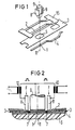
- FIG. 1 the positioning of the parts used during the method relative to a perpendicular axis 11 is shown in accordance with the method steps.
- An insulating film 3 with a working window 5 is positioned over a conductor track 4, which has a conductor track interruption 1 at a certain point, and again a molded part benefit 15 with at least one molded part 2, which is congruent with the conductor track interruption 1, is positioned over this insulating film 3.
- the exact alignment of the parts is given when the conductor interruption 1 appears in the center of the work window 5 and the molded part 2 is aligned congruently over the conductor interruption 1 and is symmetrically overlapping on both sides.
- connection process between the molded part 2 and the conductor track 4 can be carried out by means of the electron system 8; 9.
- this method provides a very specific advantage by holding the molded part 2 within the molded part benefit, in which between the process of aligning and lowering and the subsequent connection by means of resistance heating, no slipping of individual parts is possible.
- the main difference to previous methods is that the process of separating the corresponding molded part 2 from the Molded part 15 happens only after the connection process.
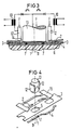
- the electrode system in this case a welding head with three electrodes 8; 9, is placed centrally on the molded part 2 in accordance with the axis 11.
- the position of the insulating film 3 is taken into account by the symmetrical position of the working window 5 with respect to the axis 11.
- the conductor track carrier 6 carries the conductor track 4, which has the conductor track interruption 1.
- the lenticular connection zones 7, which result from the connection by means of resistance heating, are placed approximately symmetrically with respect to the interruption in the conductor track 1 and arise where the spaces between the outer electrodes 8 and the inner electrode 9 are located.
- the inner electrode 9 is cylindrical and has lateral flats on the lower part, as is indicated in FIG. 1.
- the cross-section of the inner electrode 9 is adapted in accordance with the shape of the working window 5, which is also indicated in FIG. 1.
- This constructive measure also ensures protection of the adjacent conductor tracks, the spacing of which can be very small.
- the electrical supply to the electrode system 8; 9 is provided by two short-term energy sources 10, which are indicated in the form of transformers in FIG. 2. This provides short pulses, ideally vertical pulses, the current of which is, for example, 50 A with a voltage of 1 V and a pulse duration of 5 ms. Either hard soldering or welding can be carried out accordingly.
- the force F indicated in the figure, which is generated in each case by a spring, is a maximum of 0.6 N in the case of the inner electrode 9.
- the force on an outer electrode 8 is approximately one third or half of the force acting on the inner electrode 9 acts.
- FIG. 3 the same structure as in FIG. 2 is present with regard to the conductor track carrier 6, the conductor track 4, the insulating film 3 and the molded part 2.
- an electrode system 12; 13 is attached, which serves to separate out that section of the molded part 2 from the existing repair material that lies within the working window 5 and is connected to the conductor track 4.
- the outer electrodes 12 and the inner electrode 13 used in this case are dimensioned somewhat larger than the first electrode system 8; 9.
- the short-term energy sources 10, which are also used here, are decoupled by two diodes and give alternately, i.e. in succession, a short-term pulse.
- this second electrode system 12; 13 is also carried out centrally with respect to the axis 11 perpendicularly from above.
- the molded part 2 can be separated from the molded part benefit 15 at the edge of the working window 5 within the insulating film 3 by a described energy pulse.
- the separation point 14 is indicated in FIG. 3 between the left outer electrode 12 and the inner electrode 13. A time of approx. 300 ⁇ s is required for this separation process.
- the design of the electrode system has an impact on the quality of the separation process, with uniform separation with low energy expenditure being achievable by minimizing the distance between the outer electrodes 12 and the inner electrode 13 as far as possible.
- the mechanical control for positioning the individual parts is so precise that the coordinates of, for example, the axis 11 can be controlled precisely and the parts can be aligned accordingly.
- the method is monitored by means of optics, the use of a microscope being disadvantageous in that the free working space between the objective and the object is approximately 15 mm.
- the process is much easier to use if a CCD camera (Charged Coupled Device) is used.
- the height of the conductor track 4, the height of the insulating film 3 and the height of the molded part 2 are each 20 ⁇ m, for example. A range of approximately 40 ⁇ m depth can thus be observed from the surface of the molded part 2 to the surface of the conductor track 4.
- An above-mentioned camera has a depth of field of about 300 ⁇ m, thus fulfilling the optical accuracy and considerably facilitating the practical implementation of the method by the possibility of viewing the repair process on a screen.
- the advantage of using a three-electrode system as described lies in the double function of the respective inner electrode 9; 13. This is used in connection with an outer electrode 8, 12 in each case to produce a connection zone 7 or a separation point 14.
- the corresponding pulses from the short-term energy sources 10 are introduced at different times.
- controlled short-term energy sources are used, in which a target / actual value comparison for the control, i.e. ensures tracking.
- the temporal offset of the pulses between an outer electrode 8; 12 and the inner electrode 9; 13 is necessary so that the target / actual value recording is clear and there are no mutual falsifications.
- the material structure of a molded part 2 consists of a carrier layer, usually made of copper and a brazing layer usually applied by plating.
- the molded part 2 is placed on the conductor track 4 with a braze layer.
Landscapes
- Engineering & Computer Science (AREA)
- Mechanical Engineering (AREA)
- Manufacturing & Machinery (AREA)
- Microelectronics & Electronic Packaging (AREA)
- Manufacturing Of Printed Wiring (AREA)
- Electric Connection Of Electric Components To Printed Circuits (AREA)
- Structure Of Printed Boards (AREA)
- Pressure Welding/Diffusion-Bonding (AREA)
Priority Applications (1)
| Application Number | Priority Date | Filing Date | Title |
|---|---|---|---|
| AT89107071T ATE59523T1 (de) | 1988-05-26 | 1989-04-19 | Verfahren zur reparatur von leiterbahnunterbrechungen. |
Applications Claiming Priority (2)
| Application Number | Priority Date | Filing Date | Title |
|---|---|---|---|
| DE3817900 | 1988-05-26 | ||
| DE3817900 | 1988-05-26 |
Publications (2)
| Publication Number | Publication Date |
|---|---|
| EP0343375A1 true EP0343375A1 (fr) | 1989-11-29 |
| EP0343375B1 EP0343375B1 (fr) | 1990-12-27 |
Family
ID=6355167
Family Applications (1)
| Application Number | Title | Priority Date | Filing Date |
|---|---|---|---|
| EP89107071A Expired - Lifetime EP0343375B1 (fr) | 1988-05-26 | 1989-04-19 | Procédé de réparation d'interruptions dans un parcours conducteur |
Country Status (4)
| Country | Link |
|---|---|
| US (1) | US4908938A (fr) |
| EP (1) | EP0343375B1 (fr) |
| AT (1) | ATE59523T1 (fr) |
| DE (1) | DE58900037D1 (fr) |
Cited By (1)
| Publication number | Priority date | Publication date | Assignee | Title |
|---|---|---|---|---|
| EP3799522A1 (fr) * | 2019-09-26 | 2021-03-31 | Georg Emeis | Procédé et dispositif de chauffage à résistance électrique |
Families Citing this family (14)
| Publication number | Priority date | Publication date | Assignee | Title |
|---|---|---|---|---|
| US5120924A (en) * | 1990-05-16 | 1992-06-09 | Akio Hirane | Welding method for coated metal articles |
| US5060370A (en) * | 1990-10-15 | 1991-10-29 | Scales Jr James W | Modification method for etched printed circuit boards |
| US5288007A (en) * | 1991-10-04 | 1994-02-22 | International Business Machine Corporation | Apparatus and methods for making simultaneous electrical connections |
| US5243140A (en) * | 1991-10-04 | 1993-09-07 | International Business Machines Corporation | Direct distribution repair and engineering change system |
| US5193732A (en) * | 1991-10-04 | 1993-03-16 | International Business Machines Corporation | Apparatus and methods for making simultaneous electrical connections |
| US5289632A (en) * | 1992-11-25 | 1994-03-01 | International Business Machines Corporation | Applying conductive lines to integrated circuits |
| US5384953A (en) * | 1993-07-21 | 1995-01-31 | International Business Machines Corporation | Structure and a method for repairing electrical lines |
| US5904868A (en) * | 1994-06-16 | 1999-05-18 | International Business Machines Corporation | Mounting and/or removing of components using optical fiber tools |
| US6035526A (en) * | 1997-11-18 | 2000-03-14 | Ntn Corporation | Method of repairing defect and apparatus for repairing defect |
| US6651322B1 (en) * | 2000-12-28 | 2003-11-25 | Unisys Corporation | Method of reworking a multilayer printed circuit board assembly |
| EP1577046B1 (fr) * | 2004-03-18 | 2009-11-25 | Augusto Vincenzi | Méthode et appareil pour joindre un organe fonctionnel à une surface |
| BR112013007683B1 (pt) * | 2010-09-30 | 2018-05-22 | Honda Motor Co., Ltd. | "aparelho de soldagem por pontos e aparelho de soldagem do tipo alimentação indireta" |
| US8870051B2 (en) * | 2012-05-03 | 2014-10-28 | International Business Machines Corporation | Flip chip assembly apparatus employing a warpage-suppressor assembly |
| US20190366460A1 (en) * | 2018-06-01 | 2019-12-05 | Progress Y&Y Corp. | Soldering apparatus and solder nozzle module thereof |
Citations (1)
| Publication number | Priority date | Publication date | Assignee | Title |
|---|---|---|---|---|
| EP0043586A2 (fr) * | 1980-07-08 | 1982-01-13 | Siemens Aktiengesellschaft | Moyens pour réparer des discontinuités dans les conducteurs d'un circuit imprimé |
Family Cites Families (5)
| Publication number | Priority date | Publication date | Assignee | Title |
|---|---|---|---|---|
| DE2251997C3 (de) * | 1972-10-24 | 1985-03-14 | Siemens AG, 1000 Berlin und 8000 München | Verfahren zur Reparatur von schmalen Leiterbahnen elektrischer Schaltungsplatten |
| US3964666A (en) * | 1975-03-31 | 1976-06-22 | Western Electric Company, Inc. | Bonding contact members to circuit boards |
| US4259367A (en) * | 1979-07-30 | 1981-03-31 | International Business Machines Corporation | Fine line repair technique |
| GB2067845B (en) * | 1980-01-23 | 1984-04-26 | Int Computers Ltd | Manufacture of printed circuit boards |
| US4808157A (en) * | 1987-07-13 | 1989-02-28 | Neuro Delivery Technology, Inc. | Multi-lumen epidural-spinal needle |
-
1989
- 1989-03-23 US US07/327,907 patent/US4908938A/en not_active Expired - Fee Related
- 1989-04-19 AT AT89107071T patent/ATE59523T1/de not_active IP Right Cessation
- 1989-04-19 DE DE8989107071T patent/DE58900037D1/de not_active Expired - Lifetime
- 1989-04-19 EP EP89107071A patent/EP0343375B1/fr not_active Expired - Lifetime
Patent Citations (1)
| Publication number | Priority date | Publication date | Assignee | Title |
|---|---|---|---|---|
| EP0043586A2 (fr) * | 1980-07-08 | 1982-01-13 | Siemens Aktiengesellschaft | Moyens pour réparer des discontinuités dans les conducteurs d'un circuit imprimé |
Non-Patent Citations (2)
| Title |
|---|
| DESIGN ENGINEERING, Band 51, Nr. 4, Oktober 1980, Seite 23, Waseca, US; "A high-speed soldering system" * |
| IBM TECHNICAL DISCLOSURE BULLETIN, Band 14, Nr. 10, März 1972, Seite 2915, New York, US; F.M. TAPPEN: "Open conductor repair for glass metal module" * |
Cited By (1)
| Publication number | Priority date | Publication date | Assignee | Title |
|---|---|---|---|---|
| EP3799522A1 (fr) * | 2019-09-26 | 2021-03-31 | Georg Emeis | Procédé et dispositif de chauffage à résistance électrique |
Also Published As
| Publication number | Publication date |
|---|---|
| DE58900037D1 (de) | 1991-02-07 |
| EP0343375B1 (fr) | 1990-12-27 |
| ATE59523T1 (de) | 1991-01-15 |
| US4908938A (en) | 1990-03-20 |
Similar Documents
| Publication | Publication Date | Title |
|---|---|---|
| EP0343375B1 (fr) | Procédé de réparation d'interruptions dans un parcours conducteur | |
| EP0285799B1 (fr) | Dispositif de test électrique du fonctionnement de rangées de fils électriques, en particulier pour cartes de circuit | |
| DE2152081C2 (de) | Verfahren zum Anbringen von Chips mit integrierter Schaltung auf einem isolierenden Träger | |
| DE2319011A1 (de) | Verfahren zum eektrischen pruefen eines chips untereinander verbindenden leiternetzes auf einem substrat | |
| DE1950516B2 (de) | Verbindung elektrischer leiter | |
| DE1690575B2 (de) | Verfahren und einrichtung zur automatischen, lagemaessigen zentrierung eines elektronenstrahls | |
| DE3510961C2 (fr) | ||
| EP0216135B1 (fr) | Dispositif pour tester le fonctionnement électrique des interconnexions des circuits électriques, en particulier des circuits imprimés | |
| DE2841465B2 (de) | Vorrichtung zum Verschweißen von Kontaktfahnen mit Sonnenzellen | |
| EP0343374B1 (fr) | Méthode de réparation d'interruptions dans une voie conductrice au moyen d'un élément congruent | |
| DE3917750C2 (de) | Widerstandselement und Verfahren zum Abgleichen des Widerstandselementes | |
| EP0285798A2 (fr) | Dispositif de test électrique du fonctionnement de rangées de fils électriques, en particulier pour cartes de circuit | |
| EP0322607B1 (fr) | Appareil de commande pour un dispositif pour le test de platines de circuits | |
| DE4302509A1 (en) | Testing characteristics of high density circuit board - using matrix of test electrodes identical to board electrodes with precision alignment to obtain maximum inter-electrode conductivity | |
| DE3008685A1 (de) | Verfahren und vorrichtung zur einstellung der frequenzcharakteristik eines piezoelektrischen resonators | |
| DE69935963T2 (de) | Verfahren zur herstellung eines ptc-chip-varistors | |
| DE2812976C2 (de) | Verfahren zur Feststellung des Versatzes zwischen Leiterbahnen und Kontaktlöchern bei einer Leiterplatte sowie eine Leiterplatte zur Verwendung in diesem Verfahren | |
| DE3313456C2 (de) | Impuls-Lötverfahren | |
| DE2259133B2 (de) | Verfahren zum Kontaktieren einer Halbleiteranordnung und Anwendung des | |
| DE69406377T2 (de) | Bildanzeigevorrichtung und Verfahren zu ihrer Herstellung | |
| DE2354339C3 (de) | Verfahren zum Zusammenbau von Elektronenstrahlerzeugungssystemen | |
| AT393759B (de) | Kathodenstrahlroehre | |
| DE3216041A1 (de) | Elektronenstrahlerzeugungssystem mit sich selbst ausrichtenden isolierenden haltestaeben | |
| DE1639197B2 (de) | Verfahren und vorrichtung zur herstellung eines magnetisch betaetigbaren reed-schalters | |
| EP0286814A2 (fr) | Dispositif de commande |
Legal Events
| Date | Code | Title | Description |
|---|---|---|---|
| PUAI | Public reference made under article 153(3) epc to a published international application that has entered the european phase |
Free format text: ORIGINAL CODE: 0009012 |
|
| AK | Designated contracting states |
Kind code of ref document: A1 Designated state(s): AT BE CH DE FR GB IT LI NL |
|
| 17P | Request for examination filed |
Effective date: 19900110 |
|
| 17Q | First examination report despatched |
Effective date: 19900605 |
|
| GRAA | (expected) grant |
Free format text: ORIGINAL CODE: 0009210 |
|
| AK | Designated contracting states |
Kind code of ref document: B1 Designated state(s): AT BE CH DE FR GB IT LI NL |
|
| REF | Corresponds to: |
Ref document number: 59523 Country of ref document: AT Date of ref document: 19910115 Kind code of ref document: T |
|
| REF | Corresponds to: |
Ref document number: 58900037 Country of ref document: DE Date of ref document: 19910207 |
|
| ET | Fr: translation filed | ||
| ITF | It: translation for a ep patent filed | ||
| GBT | Gb: translation of ep patent filed (gb section 77(6)(a)/1977) | ||
| ITTA | It: last paid annual fee | ||
| PGFP | Annual fee paid to national office [announced via postgrant information from national office to epo] |
Ref country code: CH Payment date: 19910724 Year of fee payment: 3 |
|
| PLBE | No opposition filed within time limit |
Free format text: ORIGINAL CODE: 0009261 |
|
| STAA | Information on the status of an ep patent application or granted ep patent |
Free format text: STATUS: NO OPPOSITION FILED WITHIN TIME LIMIT |
|
| 26N | No opposition filed | ||
| PGFP | Annual fee paid to national office [announced via postgrant information from national office to epo] |
Ref country code: AT Payment date: 19920327 Year of fee payment: 4 |
|
| PGFP | Annual fee paid to national office [announced via postgrant information from national office to epo] |
Ref country code: FR Payment date: 19920428 Year of fee payment: 4 Ref country code: BE Payment date: 19920428 Year of fee payment: 4 |
|
| PG25 | Lapsed in a contracting state [announced via postgrant information from national office to epo] |
Ref country code: LI Effective date: 19920430 Ref country code: CH Effective date: 19920430 |
|
| PGFP | Annual fee paid to national office [announced via postgrant information from national office to epo] |
Ref country code: NL Payment date: 19920430 Year of fee payment: 4 |
|
| REG | Reference to a national code |
Ref country code: CH Ref legal event code: PL |
|
| PG25 | Lapsed in a contracting state [announced via postgrant information from national office to epo] |
Ref country code: GB Effective date: 19930419 Ref country code: AT Effective date: 19930419 |
|
| PG25 | Lapsed in a contracting state [announced via postgrant information from national office to epo] |
Ref country code: BE Effective date: 19930430 |
|
| BERE | Be: lapsed |
Owner name: SIEMENS A.G. Effective date: 19930430 |
|
| PG25 | Lapsed in a contracting state [announced via postgrant information from national office to epo] |
Ref country code: NL Effective date: 19931101 |
|
| GBPC | Gb: european patent ceased through non-payment of renewal fee |
Effective date: 19930419 |
|
| NLV4 | Nl: lapsed or anulled due to non-payment of the annual fee | ||
| PG25 | Lapsed in a contracting state [announced via postgrant information from national office to epo] |
Ref country code: FR Effective date: 19931229 |
|
| REG | Reference to a national code |
Ref country code: FR Ref legal event code: ST |
|
| PGFP | Annual fee paid to national office [announced via postgrant information from national office to epo] |
Ref country code: DE Payment date: 19960620 Year of fee payment: 8 |
|
| PG25 | Lapsed in a contracting state [announced via postgrant information from national office to epo] |
Ref country code: DE Free format text: LAPSE BECAUSE OF NON-PAYMENT OF DUE FEES Effective date: 19980101 |
|
| PG25 | Lapsed in a contracting state [announced via postgrant information from national office to epo] |
Ref country code: IT Free format text: LAPSE BECAUSE OF NON-PAYMENT OF DUE FEES;WARNING: LAPSES OF ITALIAN PATENTS WITH EFFECTIVE DATE BEFORE 2007 MAY HAVE OCCURRED AT ANY TIME BEFORE 2007. THE CORRECT EFFECTIVE DATE MAY BE DIFFERENT FROM THE ONE RECORDED. Effective date: 20050419 |